

Page 1
Overview
The LC72341G/W, LC72342G/W, and LC72343G/W are
single-chip microcontrollers with both a 1/4-duty 1/2-bias
LCD driver circuit and a PLL circuit that can operate at up
to 250 MHz integrated on the same chip. These ICs are
ideal for use in portable audio equipment.
Functions
• High-speed programmable divider
• Program memory (ROM)
— LC72341G/W: 2048 words × 16 bits (4KB)
— LC72342G/W: 3072 words × 16 bits (6KB)
— LC72343G/W: 4096 words × 16 bits (8KB)
• Data memory (RAM)
— LC72341G/W: 128 words × 4 bits
— LC72342G/W: 192 words × 4 bits
— LC72343G/W: 256 words × 4 bits
• Instruction cycle time
— 40 µs (for all single-word instructions.)
• Stack
— 4 levels (LC72341G/W)
— 8 levels (LC72342G/W, and LC72343G/W)
• LCD driver
— 48 to 80 segments (1/4-duty 1/2-bias drive)
• Timer interrupts
— One timer circuit providing intervals of 1, 5, 10, and
50 ms.
• External interrupts
— One external interrupt (INT)
• A/D converter
— Two channels (5-bit successive approximation)
• Input ports
— 7 (Of which two can be switched to function as A/D
converter inputs)
• Output ports
— 6 (Of which one can be switched to function as the
BEEP tone output. Two ports are open-drain ports.)
• I/O ports
— 16 (Of which 8 can be selected to function as LCD
ports as mask options.)
• PLL circuit
— Two types of dead band control are supported, and an
unlock detection circuit is included.
Reference frequencies of 1, 3, 5, 6.25, 12.5, and
25 kHz can be provided.
• Input frequency range
— FM band: 10 to 130 MHz
130 to 250 MHz
— AM band: 0.5 to 15 MHz
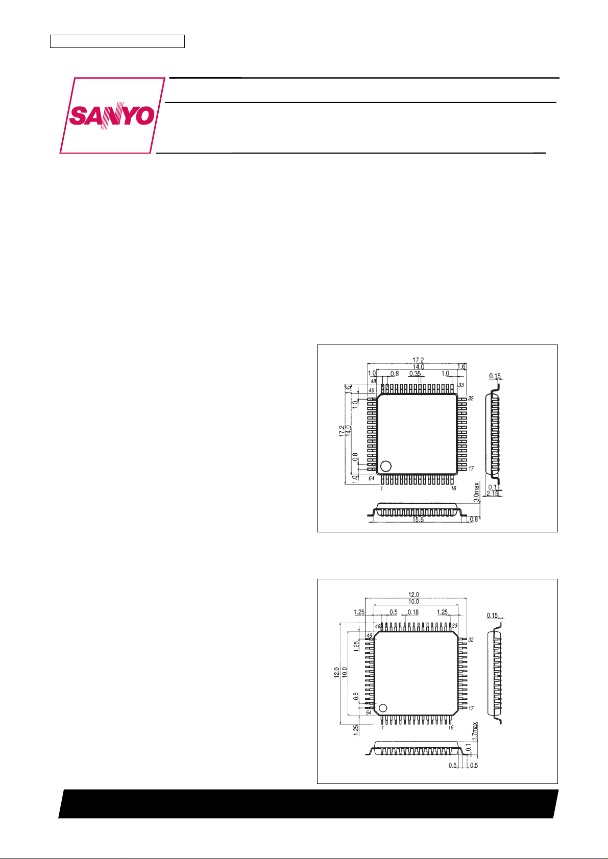
Package Dimensions
unit: mm
3159-QFP64G
unit: mm
3159-SQFP64
CMOS IC
31398RM (OT) No. 5799-1/12
Preliminary
SANYO: QFP64G
[LC72341G, 72342G, 72343G]
SANYO: SQFP64
[LC72341W, 72342W, 72343W]
SANYO Electric Co.,Ltd. Semiconductor Bussiness Headquarters
TOKYO OFFICE Tokyo Bldg., 1-10, 1 Chome, Ueno, Taito-ku, TOKYO, 110-8534 JAPAN
Low-Voltage Single-Chip Microcontrollers with On-
Chip PLL and LCD Driver Circuits
LC72341G/W, LC72342G/W, LC72343G/W
Ordering number : EN*5799
Page 2
• IF counter
— HCTR input pin; 0.4 to 12 MHz
• Voltage detection circuit (VSENSE)
— Detects the VDDvoltage and sets a flag
• External reset pin
— Restarts execution from location 0 when the CPU and PLL circuits are operating
• Power on reset circuit
— Starts execution from location 0 at power on.
• Universal counter
— 20 bits
• Beep tones
— 3.1 and 1.5 kHz
• Halt mode: The microcontroller operating clock is stopped
• Backup mode: The crystal oscillator is stopped
• An amplifier for a low-pass filter is built in
• CPU and PLL circuit operating voltage
— 1.8 to 3.6 V
• RAM data retention voltage
— 1.0 V or higher
• Packages
— QIP-64G : 0.8-mm lead pitch
— SQFP-64 : 0.5-mm lead pitch
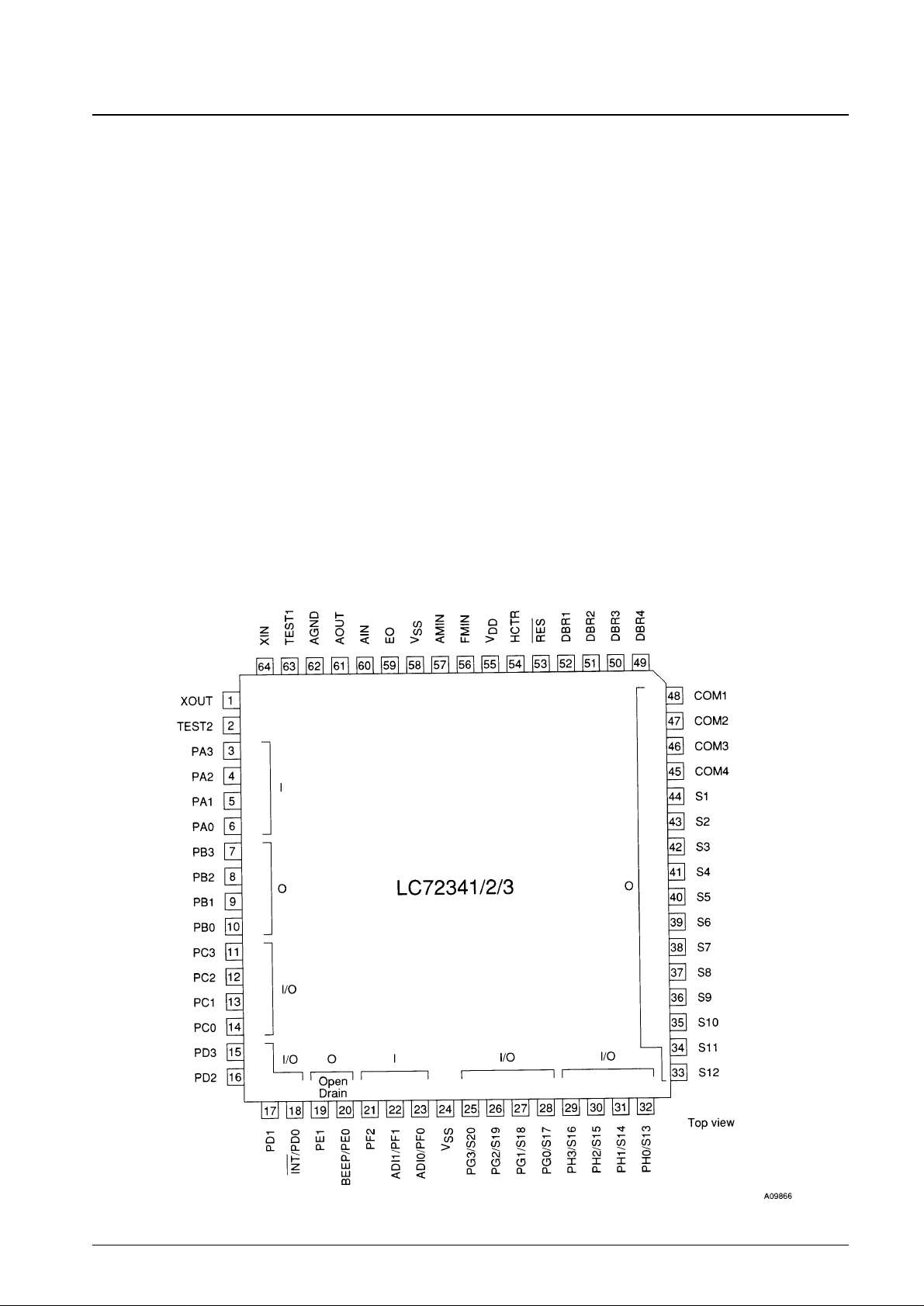
Pin Assignment
No. 5799-2/12
LC72341G/W, 72342G/W, 72343G/W
* PE0 and PE1 are open-drain outputs.
* The I/O ports can be set to input or output individually.
* The functions of the segment/general-purpose ports can be set in bit units.
Page 3
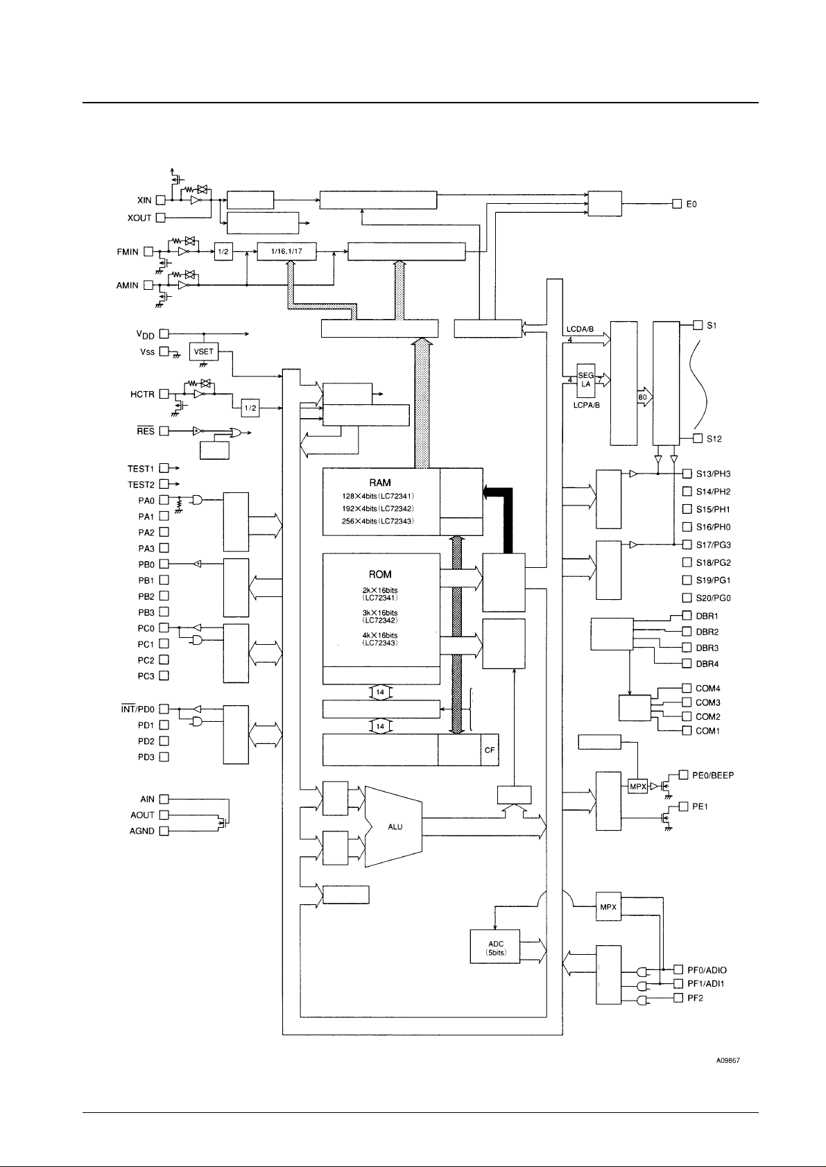
Block Diagram
No. 5799-3/12
LC72341G/W, 72342G/W, 72343G/W
Divider
Programmable divider
PLL data latch
PLL control
count end
Reference divider
Phase-
detector
System clock
generator
Time base
control
Pon
reset
Bus
driver
Data
latch/
Bus
driver
Data
latch/
Bus
driver
Address decoder
Program counter
Stack
Timer 0
Judge
Beep tone
Latch
A
Latch
B
JMP CAL
Return
interrupt
reset
Doubler
circuit
Common
driver
Instruction
decoder
Bus
control
Address
decoder
LCD
Port
driver
Lach
Bank
Skip
Bank
Data
latch/
Bus
driver
Data
latch/
Bus
driver
Data
latch/
Bus
driver
Data
latch/
Bus
driver
Data
latch/
Bus
driver
Universal counter
(20 bits)
Data bus
Page 4
No. 5799-4/12
LC72341G/W, 72342G/W, 72343G/W
Parameter Symbol Conditions Ratings Unit
Maximum supply voltage V
DD
max –0.3 to +4.0 V
Input voltage V
IN
All input pins –0.3 to VDD+ 0.3 V
Output voltage
V
OUT
1 AOUT, PE –0.3 to +15 V
V
OUT
2 All output pins except V
OUT
1 –0.3 to VDDto + 0.3 V
I
OUT
1 PC, PD, PG, PH, EO 0 to 3 mA
I
OUT
2 PB 0 to 1 mA
Output current I
OUT
3 AOUT, PE 0 to 2 mA
I
OUT
4 S1 to S20 300 µA
I
OUT
5 COM1 to COM4 3 mA
Allowable power dissipation Pd max Ta = –20 to +70°C 300 mW
Operating temperature Topr –20 to +70 °C
Storage temperature Tstg –45 to +125 °C
Specifications
Absolute Maximum Ratings at Ta = 25°C, VSS= 0 V
Parameter Symbol Conditions
Ratings
Unit
min typ max
Supply voltage
V
DD
1 CPU and PLL operating voltage 1.8 3.0 3.6 V
V
DD
2 Memory retention voltage 1.0 V
V
IH
1
V
IH
2, VIH3, AMIN, FMIN,
0.7 V
DD
V
DD
V
Input high-level voltage
Input ports except HCTR and XIN.
V
IH
2 RES 0.8 V
DD
V
DD
V
V
IH
3 Port PF 0.6 V
DD
V
DD
V
V
IL
1
V
IL
2, VIL3, AMIN, FMIN,
0 0.3 V
DD
V
Input low-level voltage
Input ports except HCTR and XIN.
V
IL
2 RES 0 0.2 V
DD
V
V
IL
3 Port PF 0 0.2 V
DD
V
V
IN
1 XIN 0.5 0.6 Vrms
Input amplitude
V
IN
2 FMIN, AMIN 0.035 0.35 Vrms
V
IN
3 FMIN 0.05 0.35 Vrms
V
IN
4 HCTR 0.035 0.35 Vrms
Input voltage range V
IN
5 ADI0, ADI1 0 V
DD
V
F
IN
1 XIN : CI ≤ 35 kΩ 70 75 80 kHz
F
IN
2 FMIN : VIN2, VDD1 10 130 MHz
Input frequency
F
IN
3 FMIN : VIN3, VDD1 130 250 MHz
F
IN
4 AMIN (H) : VIN2, VDD1 2 40 MHz
F
IN
5 AMIN (L) : VIN2, VDD1 0.5 10 MHz
F
IN
6 HCTR : VIN4, VDD1 0.4 12 MHz
Allowable Operating Ranges at Ta = –20 to 70°C, VDD= 1.8 to 3.6 V
Parameter Symbol Conditions
Ratings
Unit
min typ max
I
IH
1 XIN: VI= VDD= 3.0 V 3 µA
Input high-level current
I
IH
2 FMIN, AMIN, HCTR : VI= VDD= 3.0 V 3 8 20 µA
I
IH
3
Ports PA/PF (with no pull-down resistor), PC,
3 µA
PD, PG, and PH. RES: V
I
= VDD= 3.0 V
I
IL
1 XIN : VI= VDD= V
SS
–3 µA
Input low-level current
I
IL
2 FMIN, AMIN, HCTR : VI= VDD= V
SS
–3 –8 –20 µA
I
IL
3
Ports PA/PF (with no pull-down resistor), PC,
–3 µA
PD, PG, and PH. RES: V
I
= VDD= V
SS
Input floating voltage V
IF
PA/PF with pull-down resistors used 0.05 V
DD
V
Pull-down resistance R
PD
1
PA/PF with pull-down resistors used, VDD= 3 V
75 100 200 kΩ
Hysteresis V
H
RES 0.1 V
DD
0.2 V
DD
V
Voltage doubler reference voltage DBR4 Ta = 25°C, referenced to V
DD
, C3 = 0.47 µF 1.3 1.5 1.7 V
Voltage doubler step-up voltage DBR1, 2, 3
Ta = 25°C, C1 = 0.45 µF, C2 = 0.47 µF, no load
2.7 3.0 3.3 V
Electrical Characteristics at Ta = –20 to 70°C, VDD= 1.8 to 3.6 V (in the allowable operating ranges)
Page 5

No. 5799-5/12
LC72341G/W, 72342G/W, 72343G/W
Note: C1, C2, and C3 must be provided even if no LCD is used.
Note: 1. Capacitors C1, C2, and C3 must be connected to the DBR pins.
Note: The halt mode current is measured with the CPU executing 20 instructions every 125 ms.
Parameter Symbol Conditions
Ratings
Unit
min typ max
V
OH
1 PB : IO= –1 mA
VDD– 0.7 V
DD
V
V
OH
2 PC, PD, PG, PH : IO= –1 mA
VDD– 0.3 V
DD
V
V
OH
3 EO : IO= –500 µA
VDD– 0.3 V
DD
V
Output high-level voltage V
OH
4 XOUT : IO= –200 µA
VDD– 0.3 V
DD
V
V
OH
5 S1 to S20 : IO= –20 µA: *1 2.0 V
V
OH
6
COM1, COM2, COM3, COM4:
2.0 V
I
O
= –100 µA : *1
V
OL
1 PB : IO= –50 µA 0.7 V
DD
V
V
OL
2 PC, PD, PE, PG, PH : IO= –1 mA 0.3 V
DD
V
V
OL
3 EO : IO= –500 µA 0.3 V
DD
V
V
OL
4 XOUT : IO= –200 µA 0.3 V
DD
V
Output low-level voltage V
OL
5 S1 to S20 : IO= –20 µA: *1 1.0 V
V
OL
6
COM1, COM2, COM3, COM4 :
1.0 V
I
O
= –100 µA : *1
V
OL
7 PE : IO= 5 mA 1.0 V
V
OL
8 AOUT : IO= 1 mA, AIN = 1.3 V, VDD= 3 V 0.5 V
Output off leakage current
I
OFF
1 Ports PB, PC, PD, PG, PH, and EO –3 +3 µA
I
OFF
2 Ports AOUT and PE –100 +100 nA
A/D conversion error ADI0, ADI1, V
DD
= VDD1 –1/2 +1/2 LSB
Electrical Characteristics at Ta = –30 to 70°C, VDD= 1.8 to 3.6 V (in the allowable operating ranges)
Parameter Symbol Conditions
Ratings
Unit
min typ max
Falling supply voltage detection voltage V
SENSE
1 Ta = 25°C *2 1.6 1.75 1.9 V
Rising supply voltage detection voltage V
SENSE
2 Ta = 25°C *2
VSENSE1 +0.1 VSENSE1 +0.2
V
Pull-down resistance R
PD
2 TEST1, TEST2 10 kΩ
I
DD
1 VDD1 : FIN2 130 MHz, Ta = 25°C 10 mA
I
DD
2 VDD2: In halt mode at Ta = 25°C, *3 0.1 mA
Supply current I
DD
3
V
DD
= 3.6 V, with the oscillator stopped,
1 µA
at Ta = 25°C, *4
I
DD
4
V
DD
= 1.8 V, with the oscillator stopped,
0.5 µA
at Ta = 25°C, *4
Electrical Characteristics at Ta = –20 to 70°C, VDD= 1.8 to 3.6 V (in the allowable operating ranges)
Page 6

No. 5799-6/12
LC72341G/W, 72342G/W, 72343G/W
When the Supply Voltage is Falling
When the Supply Voltage is Rising
Note: 3. Halt Mode Current Test Circuit
Note: 4. Backup Mode Current Test Circuit
All ports other than those specified in the figure
must be left open.
Set ports PC and PD to output.
Select segments S13 to S20.
All ports other than those specified in the figure
must be left open.
Set ports PC and PD to output.
Select segments S13 to S20.
Note: 2. The V
SENSE
voltage
When the V
DD
voltage falls, the V
SENSE
flag is set at the point that voltage falls under 1.75 V (typical). The TST instruction can be used to read the
value of the V
SENSE
flag. Applications can easily determine when the batteries are exhausted by monitoring this flag. After V
SENSE
is set when the
supply voltage falls, it will not be reset if the supply voltage rises by less than 0.1 V, because the voltages detected by the V
SENSE
circuit differ when
the supply voltage is falling and when the supply voltage is rising.
Page 7

No. 5799-7/12
LC72341G/W, 72342G/W, 72343G/W
Pin Functions
Pin No. Pin I/O Function I/O circuit
64
1
XIN
XOUT
I
O
Connections for a 75-kHz crystal oscillator element
63
2
TEST1
TEST2
I
I
IC test pins. These pins must be tied to ground.
Input with built-in pull-
down resistor
6
5
4
3
PA0
PA1
PA2
PA3
I
Special-purpose key return signal input ports designed with a low threshold voltage.
When used in conjunction with port PB to form a key matrix, up to 3 simultaneous key
presses can be detected. The four pull-down resistors are selected together in a single
operation using the IOS instruction (PWn = 2, b1); they cannot be specified individually.
Input is disabled in backup mode, and the pull-down resistors are disabled after a reset.
Unbalanced CMOS
push-pull circuit
10
9
8
7
PB3
PB2
PB1
PB0
O
Special-purpose key source signal output ports. Since unbalanced CMOS output
transistor circuits are used, diodes to prevent short-circuits when multiple keys are
pressed are not required. These ports go to the output high-impedance state in backup
mode. These ports go to the output high-impedance state after a reset and remain in that
state until an output instruction (OUT, SPB, or RPB) is executed.
Care is required in designing the output loads if these pins are used for functions other
than key source outputs.
CMOS push-pull circuit
14
13
12
11
18
17
16
15
PC0
PC1
PC2
PC3
INT/PD0
PD1
PD2
PD3
I/O
General-purpose I/O ports*. PD0 can be used as an external interrupt port. Input or
output mode can be set in a bit unit using the IOS instruction (Pwn = 4, 5). A value of 0
specifies input, and 1 specifies output. These ports go to the input disabled highimpedance state in backup mode. They are set to function as general-purpose input ports
after a reset.
N-channel open drain
20
19
BEEP/PE0
PE1
General-purpose output ports with shared beep tone output function (PE0 only). The
BEEP instruction is used to switch PE0 between the general-purpose output port and
beep tone output functions. To use PE0 as a general-purpose output port, execute a
BEEP instruction with b2 set to 0. Set b2 to 1 to use PE0 as the beep tone output port.
The b0 and b1 bits are used to select the beep tone frequency. There are two beep tone
frequencies supported.
When PE0 is set up as the beep tone output, executing an output instruction to PN0 only
changes the state of the internal output latch, it does not affect the beep tone output in
any way. Only the PE0 pin can be switched between the general-purpose output
function and the beep tone output function; the PE1 pin only functions as a generalpurpose output. These pins go to the high-impedance state in backup mode and remain
in that state until an output instruction or a BEEP instruction is executed. Since these
ports are open-drain ports, resistors must be inserted between these pins and V
DD
.
These ports are set to their general-purpose output port function after a reset.
CMOS input/analog
input
23
22
21
PF0/ADI0
PF1/ADI1
PF2
I
General-purpose input and A/D converter input shared function ports (PF2 is a generalpurpose input only port). The IOS instruction (Pwn = FH) is used to switch between the
general-purpose input and A/D converter port functions. The general-purpose input and
A/D converter port functions can be switched in a bit unit, with 0 specifying generalpurpose input, and 1 specifying the A/D converter input function. To select the A/D
converter function, set up the A/D converter pin with an IOS instruction with Pwn set to 1.
The A/D converter is started with the UCC instruction (b3 = 1, b2 = 1). The ADCE flag is
set when the conversion completes. The INR instruction is used to read in the data.
If an input instruction is executed for one of these pins which is set up for analog input,
the read in data will be at the low level since CMOS input is disabled. In backup mode
these pins go to the input disabled high-impedance state. These ports are set to their
general-purpose input port function after a reset. The A/D converter is a 5-bit successive
approximation type converter, and features a conversion time of 1.28 ms. Note that the
full-scale A/D converter voltage (1FH) is (63 · 96)V
DD
.
Continued on next page.
Note: * Applications must establish the output data in advance with an OUT, SPB, or RPB instruction and then set the pin to output mode with an IOS
instruction when using the I/O switchable ports as output pins.
Page 8

No. 5799-8/12
LC72341G/W, 72342G/W, 72343G/W
Continued from preceding page.
Pin No. Pin I/O Function I/O circuit
25
26
27
28
29
30
31
32
PG3/S20
PG2/S19
PG1/S18
PG0/S17
PH3/S16
PH2/S15
PH1/S14
PH0/S13
I/O
LCD driver segment output and general-purpose I/O shared function ports. The IOS
instruction is used for switching both between the segment output and general-purpose
I/O functions and between input and output for the general-purpose I/O port function.*
• When used as segment output ports
The general-purpose I/O port function is selected with the IOS instruction (Pwn = 8).
b0 = S17 to 20/PG0 to 3 (0: Segment output, 1: PG0 to 3)
The general-purpose I/O port function is selected with the IOS instruction (Pwn = 9).
b0 = S13 to 16/PH0 to 3 (0: Segment output, 1: PH0 to 3)
• When used as general-purpose I/O ports
The IOS instruction (Pwn = 6,7) is used to select input or output. Note that the mode can
be set in a bit unit.
b0 = PG0 b0 = PH0
b1 = PG1
[0: Input, 1: Output]
b1 = PH1
[0: Input, 1: Output]
b2 = PG2 b2 = PH2
b3 = PG3 b3 = PH3
In backup mode, these pins go to the input disabled, high-impedance state if set up as
general-purpose outputs, and are fixed at the low level if set up as segment outputs.
These ports are set up as segment outputs after a reset.
Although the general-purpose port/LCD port setting is a mask option, the IOS instruction
must be used as described above to set up the port function.
CMOS push-pull circuit
S16 to
S1
33 to 44 O
LCD driver segment output pins.
A 1/4-duty 1/2-bias drive technique is used.
The frame frequency is 75 Hz.
In backup mode, the outputs are fixed at the low level.
After a reset, the outputs are fixed at the low level.
CMOS push-pull circuit
COM4
COM3
COM2
COM1
45
46
47
48
O
LCD driver common output pins.
A 1/4-duty 1/2-bias drive technique is used.
The frame frequency is 75 Hz.
In backup mode, the outputs are fixed at the low level.
After a reset, the outputs are fixed at the low level.
DBR4
DBR3
DBR2
DBR1
49
50
51
52
LCD power supply stepped-up voltage pins.
53 RES I
System reset input.
In CPU operating mode or halt mode, applications must apply a low level for at least one
full machine cycle to reset the system and restart execution with the PC set to location 0.
This pin is connected in parallel with the internal power on reset circuit.
70 HCTR I
Universal counter dedicated input port.
• When taking frequency measurements, select the HCTR frequency measurement mode
and measurement time with the UCS instruction (b3 = 0, b2 = 0) and start the count with
a UCCinstruction.
The CNTEND flag is set when the count completes. Since this circuit functions as an AC
amplifier, always use capacitor coupling with the input signal. Input is disabled in backup
mode, in halt mode, after a reset, and in PLL stop mode.
UCS b3, b2 Input pin Measurement mode
0 0 HCTR Frequency measurement
0 1 —
1 0 —
1 1 —
UCS b1, b0 Measurement time
0 0 1 ms
0 1 4 ms
1 0 8 ms
1 1 32 ms
Continued on next page.
CMOS input/analog
input
Note: * Applications must establish the output data in advance with an OUT, SPB, or RPB instruction and then set the pin to output mode with an IOS
instruction when using the I/O switchable ports as output pins.
Page 9

No. 5799-9/12
LC72341G/W, 72342G/W, 72343G/W
Pin No. Pin I/O Function I/O circuit
56 FMIN I
FM VCO (local oscillator) input.
This pin is selected with the PLL instruction CW1.
The input must be capacitor coupled.
Input is disabled in backup mode, in halt mode, after a reset, and in PLL stop mode.
57 AMIN I
AM VCO (local oscillator) input.
This pin and the bandwidth are selected with the PLL instruction CW1.
The input must be capacitor coupled.
Input is disabled in backup mode, in halt mode, after a reset, and in PLL stop mode.
59 E0 O
The main charge pump output. When the local oscillator frequency divided by N is higher
than the reference frequency a high level is output, when lower, a low level is output, and
the pin is set to the high-impedance state when the frequencies match.
Output goes to the high-impedance state in backup mode, in halt mode, after a reset, and
in PLL stop mode.
60
61
62
AIN
AOUT
AGND
O
Transistor used for the low-pass filter amplifier.
Connect AGND to ground.
24
58
55
V
SS
V
SS
V
DD
—
—
—
Power supply pin. This pin must be connected to ground.
Power supply pin. This pin must be connected to ground.
Power supply pin. This pin must be connected to V
DD
.
Continued from preceding page.
CW1 b1, b0 Bandwidth
1 0 2 to 40 MHz (SW)
1 1 0.5 to 10 MHz (MW, LW)
CMOS amplifier input
CMOS amplifier input
Push-pull CMOS
output
Handling of Unused Pins
Pin No. Pin I/O type Pin handling
3 to 6 PA port I Connect to V
DD
or VSS. May be left open if the pull-up resistor is selected with the IOS instruction.
7 to 10 PB port O Open
11 to 14 PC port I/O Connect to V
DD
or VSSwhen input is selected. Leave open if output is selected.
15 to 18 PD port I/O Connect to V
DD
or VSSwhen input is selected. Leave open if output is selected.
19, 20 PE port O Open
21 to 23 PF port I
Connect to VDDor VSS. The PF2 pin only may be left open if the pull-up resistor is selected with the IOS instruction.
25 to 28 PG/S ports I/O/S Connect to VDDor VSSwhen input is selected. Leave open if output or LCD operation is selected.
29 to 32 PH/S ports I/O/S Connect to V
DD
or VSSwhen input is selected. Leave open if output or LCD operation is selected.
33 to 41 S port O Open
45 to 48 COM O Open
49 DBR1 — Connect to DBR2 through a capacitor.
50 DBR2 — Connect to DBR1 through a capacitor.
51 DBR3 — Connect to V
SS
through a capacitor.
52 DBR4 — Connect to V
SS
through a capacitor.
53 RES I V
DD
54 HCTR I VSSLeave open if FMIN is used.
56 FMIN I V
SS
57 AMIN I V
SS
59 EO O Open
60 AIN I V
SS
61 AOUT O Open
63 TEST1 I Connect to V
SS
or leave open. Connection to VSSis preferable.
2 TEST2 I Connect to V
SS
or leave open. Connection to VSSis preferable.
Page 10

No. 5799-10/12
LC72341G/W, 72342G/W, 72343G/W
Mask Options
Development Environment and Tools
• The LC72P341 is available as a OTP version.
• The LC72EV340 is available as an evaluation chip.
• A total debugging system is formed by the combination of the TB-72EV32 evaluation chip board, the RE32 multifunction emulator, and a personal computer for system control.
Port Selection
1 PG3/S20 General-purpose port LCD port
2 PG2/S19 General-purpose port LCD port
3 PG1/S18 General-purpose port LCD port
4 PG0/S17 General-purpose port LCD port
5 PH3/S16 General-purpose port LCD port
6 PH2/S15 General-purpose port LCD port
7 PH1/S14 General-purpose port LCD port
8 PH0/S13 General-purpose port LCD port
Page 11

No. 5799-11/12
LC72341G/W, 72342G/W, 72343G/W
Instruction Set
Instruction
Mnemonic
Opcode Machine code
Operation
group 1st 2nd 15 12 11 8 7 4 3 0
AD r M 0100 00 DH DL r r ← (r) + (M)
ADS r M 0100 01 DH DL r r ← (r) + (M), skip if carry
AC r M 0100 10 DH DL r r ← (r) + (M) + C
ACS r M 0100 11 DH DL r r ← (r) + (M) + C, skip if carry
AI M I 0101 00 DH DL I M ← (M) + I
AIS M I 0101 01 DH DL I M ← (M) + I, skip if carry
AIC M I 0101 10 DH DL I M ← (M) + I + C
AICS M I 0101 11 DH DL I M ← (M) + I + C, skip if carry
SU r M 0110 00 DH DL r r ← (r) – (M)
SUS r M 0110 01 DH DL r r ← (r) – (M), skip if borrow
SB r M 0110 10 DH DL r r ← (r) – (M) – b
SBS r M 0110 11 DH DL r r ← (r) – (M) – b, skip if borrow
SI M I 0111 00 DH DL I M ← (M) – I
SIS M I 0111 01 DH DL I M ← (M) – I, skip if borrow
SIB M I 0111 10 DH DL I M ← (M) – I – b
SIBS M I 0111 11 DH DL I M ← (M) – I – b, skip if borrow
SEQ r M 0001 00 DH DL r (r) ← (M), skip if zero
SEQI M I 0001 10 DH DL I (M) — I, skip if zero
SNEI M I 0000 01 DH DL I (M) — I, skip if not zero
SGE r M 0001 10 DH DL r (r) — (M), skip if not borrow
SGEI M I 0001 11 DH DL I (M) — I, skip if not borrow
SLEI M I 0000 11 DH DL I (M) — I, skip if borrow
ANDI M I 0010 01 DH DL I M ← (M) AND I
ORI M I 0010 11 DH DL I M ← (M) OR I
EXLI M I 0011 10 DH DL I M ← (M) XOR I
AND r M 0010 00 DH DL r r ← (r) AND M
OR r M 0010 10 DH DL r r ← (r) OR M
EXL r M 0011 00 DH DL r r ← (r) XOR M
SHR r 0000 00 00 1110 r Shift r right with carry
LD r M 1101 00 DH DL r r ← (M)
ST M r 1101 01 DH DL r M ← (r)
MVRD r M 1101 10 DH DL r [DH, rn] ← (M)
MVRS M r 1101 11 DH DL r M ← [DH, rn]
MVSR M1 M2 1110 00 DH DL1 DL2 [DH, DL1] ← [DH, DL2]
MVI M I 1110 01 DH DL I M ← I
TMT M N 1111 00 DH DL N if M (N) = all 1, then skip
TMF M N 1111 01 DH DL N if M (N) = all 0, then skip
JMP ADDR 100 ADDR (13 bits) PC ← ADDR
CAL ADDR 101 ADDR (13 bits) PC ← ADDR, Stack ← (PC) + 1
RT 0000 0000 1000 PC ← Stack
RTI 0000 0000 1001 PC ←Stack, BANK ←Stak, carry ←stack
SS I N 1111 1111 000 I N (Status reg. I)N ← 1
RS I N 1111 1111 001 I N (Status reg. I)N ← 0
TST I N 1111 1111 01 I N if (Status reg. I)N = all 1, then skip
TSF I N 1111 1111 10 I N if (Status reg. I)N = all 0, then skip
TUL N 0000 0000 1101 N if Unlock F/F (N) = all 0, then skip
Addition instructionsSubtraction instructions
Comparison
instructions
Logic and arithmetic
instructions
Transfer instructions
Jump and
subroutine
call
instructions
Status register
test and flip-flop
control
instructions
Memory
test
instructions
Continued on next page.
Page 12

PS No. 5799-12/12
LC72341G, W, LC72342G, W, LC72343G, W
This catalog provides information as of March, 1998. Specifications and information herein are subject to
change without notice.
■ No products described or contained herein are intended for use in surgical implants, life-support systems, aerospace
equipment, nuclear power control systems, vehicles, disaster/crime-prevention equipment and the like, the failure of
which may directly or indirectly cause injury, death or property loss.
■ Anyone purchasing any products described or contained herein for an above-mentioned use shall:
➀ Accept full responsibility and indemnify and defend SANYO ELECTRIC CO., LTD., its affiliates, subsidiaries and
distributors and all their officers and employees, jointly and severally, against any and all claims and litigation and all
damages, cost and expenses associated with such use:
➁ Not impose any responsibility for any fault or negligence which may be cited in any such claim or litigation on
SANYO ELECTRIC CO., LTD., its affiliates, subsidiaries and distributors or any of their officers and employees
jointly or severally.
■ Information (including circuit diagrams and circuit parameters) herein is for example only; it is not guaranteed for
volume production. SANYO believes information herein is accurate and reliable, but no guarantees are made or implied
regarding its use or any infringements of intellectual property rights or other rights of third parties.
Instruction
Mnemonic
Opcode Machine code
Operation
group 1st 2nd 15 12 11 8 7 4 3 0
PLL M r 1111 10 DH DL r PLL reg. ← PLL data
TMS I 0000 0000 1100 I Timer reg. ← I
UCS I 0000 0000 0001 I UCS reg. ← I
UCC I 0000 0000 0010 I UCC reg. ← I
BEEP I 0000 0000 0110 I BEEP reg. ← I
DZC I 0000 0000 1011 I DZC reg. ← I
BANK I 0000 0000 0111 I BANK ← I
IOS Pn I 1111 1110 Pn I IOS reg. Pn ← I
INR M Rn 0011 10 DH DL r M ← (Rn reg.)
IN M Pn 1110 10 DH DL Pn M ← (Pn)
OUT M Ph 1110 11 DH DL Pn Pn ← M
SPB Pn N 0000 0010 Pn N (Pn) N ← 1
RPB Pn N 0000 0011 Pn N (Pn) N ← 0
TPT Pn N 1111 1100 Pn N if (Pn) N = all 1, then skip
TPF Pn N 1111 1101 Pn N if (Pn) N = all 0, then skip
LCDA M I 1100 00 DH DL DIGIT LCD (DIGIT) ← M
LCDB M I 1100 01 DH DL DIGIT
LCPA M I 1100 10 DH DL DIGIT LCD (DIGIT) ← Logic
LCPB M I 1100 11 DH DL DIGIT Array ← M
HALT I 0000 0000 0100 I HALT reg. ← I, then CPU Stop
CKSTP 0000 0000 0101 Stop Xtal OSC
NOP 0000 0000 0000 No operation
Peripheral hardware control
instructions
I/O instructions
LCD control
instructions
Other
instructions
Continued from preceding page.
 Loading...