

Page 1

Overview
The LC72336 and LC72338 are single-chip
microcontrollers for use in electronic tuners. These
products include on chip a PLL circuit that can operate at
up to 150 MHz and 1/3 duty LCD drivers. They feature a
highly efficient instruction set and powerful hardware.
Functions
• High-speed programmable divider
• Program memory (ROM)
— LC72336: 6143 × 16 bits (12 kB)
— LC72338: 8191 × 16 bits (16 kB)
• Data memory (RAM): 512 × 4 bits
• All instructions are one-word instructions
• Cycle time: 1.33 µs
• Stack: 8 levels
• LCD drivers: Up to 96 segments (1/3 duty, 1/3 bias)
• Serial I/O: Up to 3 channels (8-bit 3-wire type)
• External interrupts: 2 interrupts (INT0, INT1)
Interrupt on rising or falling edge (selectable)
• Internal interrupts: 3 interrupt
Two built-in timer interrupts and 1 serial I/O interrupt
• Nested interrupt levels: 4 levels
• D/A converter: 4 channels (8-bit PWM output)
• A/D converter: 4 channels
(6-bit successive approximation)
• General-purpose ports:
— Input ports: 8
— Output ports: 12 (16 maximum)
— I/O ports: 8 (20 maximum, can be switched between
input and output in bit units.)
• PLL block: Supports 4 types of dead zone control, and
includes a built-in unlock detection circuit.
Supports 12 different reference frequencies.
• Universal counter: 20 bits (Can be used for either
frequency or period measurement.)
• Timers: Eight types of time measurement
• Beep function: Six beep tones
• Reset: Built-in voltage detection type reset circuit
• Halt mode: Stops the controller operating clock.
• Operating supply voltage: 4.5 to 5.5 V (3.5 to 5.5 V if
only the controller block operates.)
Package Dimensions
unit: mm
3174-QFP80E
CMOS LSI
Ordering number : EN5157C
O3097HA (OT)/13095HA (OT) No. 5157-1/16
SANYO: QIP80E
[LC72336, 72338]
SANYO Electric Co.,Ltd. Semiconductor Bussiness Headquarters
TOKYO OFFICE Tokyo Bldg., 1-10, 1 Chome, Ueno, Taito-ku, TOKYO, 110 JAPAN
Single-Chip Microcontrollers
with Built-In LCD Driver and PLL Circuits
LC72336, 72338
This LSI can easily use CCB that is SANYO’s original bus format.
• CCB is a trademark of SANYO ELECTRIC CO., LTD.
• CCB is SANYO’s original bus format and all the bus
addresses are controlled by SANYO.
Page 2
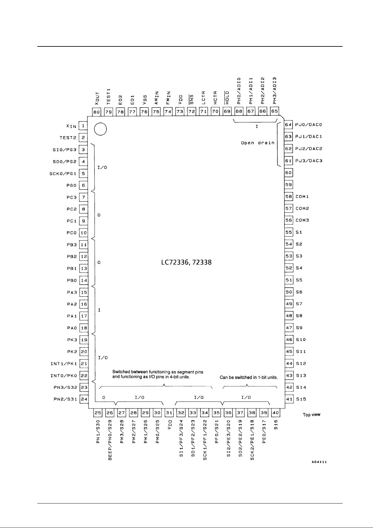
Pin Assignment
No. 5157-2/16
LC72336, 72338
V
dd1
V
dd2
Page 3
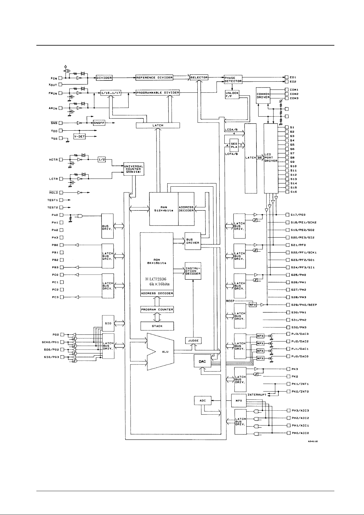
Block Diagram
No. 5157-3/16
LC72336, 72338
V
dd1
V
dd2
Page 4
Specifications
Absolute Maximum Ratings at Ta = 25°C, VSS= 0 V
Note: * Reference value
Allowable Operating Ranges at Ta = –40 to +85°C, VDD= 3.5 to 5.5 V
No. 5157-4/16
LC72336, 72338
Parameter Symbol Conditions Ratings Unit
Maximum supply voltage V
DD
max –0.3 to +6.5 V
Input voltage V
IN
All input pins –0.3 to VDD+ 0.3 V
Output voltage
V
OUT
(1) Port PJ –0.3 to +15 V
V
OUT
(2) All output ports other than V
OUT
(1) –0.3 to VDD+ 0.3 V
I
OUT
(1) Port PJ 0 to +5 mA
I
OUT
(2) PE, PF, PG, PK, PM, PN, EO1, EO2 0 to +3 mA
Output current I
OUT
(3) Ports PB and PC 0 to +1 mA
I
OUT
(4) S1 to S32 300 µA
I
OUT
(5) COM1 to COM3 3 mA
Allowable power dissipation Pd max Ta = –45 to 85°C 300 mW*
Operating temperature Topr –40 to +85 °C
Storage temperature Tstg –45 to +125 °C
Parameter Symbol Conditions min typ max Unit
V
DD
(1) CPU and PLL operating 4.5 5.0 5.5 V
Supply voltage V
DD
(2) CPU operating 3.5 5.5 V
V
DD
(3) Memory retention 1.3 5.5 V
V
IH
(1)
Ports PE, PH, and PM,
0.7 V
DD
V
DD
V
HCTR and LCTR (when selected for input)
Input high-level voltage
V
IH
(2)
Ports PF, PG, and PK,
0.8 V
DD
V
DD
V
LCTR (frequency measurement mode), and HOLD
V
IH
(3) SNS 2.5 V
DD
V
V
IH
(4) Port PA 0.6 V
DD
V
DD
V
V
IL
(1)
Port PE, PH, and PM,
0 0.3 V
DD
V
HCTR and LCTR (when selected for input)
Input low-level voltage
V
IL
(2)
Port PA, PF, PG, and PK,
0 0.2 V
DD
V
LCTR (frequency measurement mode)
V
IL
(3) SNS 0 +1.3 V
V
IL
(4) HOLD 0 0.4 V
DD
V
f
IN
(1) XIN 4.0 4.5 5.0 MHz
f
IN
(2) FMIN: VIN(2), VDD(1) 10 150 MHz
f
IN
(3) FMIN: VIN(3), VDD(1) 10 130 MHz
f
IN
(4) AMIN (H): VIN(3), VDD(1) 2.0 40 MHz
Input frequency
f
IN
(5) AMIN (L): VIN(3), VDD(1) 0.5 10 MHz
f
IN
(6) HCTR: VIN(3), VDD(1) 0.4 12 MHz
f
IN
(7) LCTR: VIN(3), VDD(1) 100 500 kHz
f
IN
(8)
LCTR (frequency measurement mode):
1 20 × 10
3
Hz
V
IH
(2), VIL(2), VDD(1)
V
IN
(1) XIN 0.5 1.5 Vrms
Input amplitude V
IN
(2) FMIN 0.10 1.5 Vrms
V
IN
(3) FMIN, AMIN, HCTR, LCTR 0.07 1.5 Vrms
Input voltage range V
IN
(4) ADI0 to ADI3 0 V
DD
V
Page 5
Electrical Characteristics for the Allowable Operating Ranges
Note: * In case of instruction execution for 20 steps at intervals of 1 ms, with the PLL, counter functions and other functions all stopped.
No. 5157-5/16
LC72336, 72338
Parameter Symbol Conditions min typ max Unit
I
IH
(1) XIN: VI= VDD= 5.0 V 2.0 5.0 15 µA
I
IH
(2) FMIN, AMIN, HCTR, LCTR: VI= VDD= 5.0 V 4.0 10 30 µA
Ports PA, PE, PF, PG, PH, PK, and PM, SNS, HOLD,
Input high-level current
I
IH
(3)
HCTR, LCTR: No pull-down resistors on port PA,
3.0 µA
V
I
= VDD= 5.0 V, with input mode selected
for ports PE, PF, PG, PK, and PM
IIH(4) With pull-down resistors on port PA, VI= VDD= 5.0 V 50 µA
I
IL
(1) XIN: VI= V
SS
2.0 5.0 15 µA
I
IL
(2) FMIN, AMIN, HCTR, LCTR: VI= V
SS
4.0 10 30 µA
Input low-level current
Ports PA, PE, PF, PG, PH, PK, and PM, SNS, HOLD,
I
IL
(3)
HCTR, LCTR: No pull-down resistors on port PA,
3.0 µA
V
I
= VSS, with input mode selected
for ports PE, PF, PG, PK, and PM
Input floating voltage V
IF
With pull-down resistors on port PA 0.05 V
DD
V
Pull-down resistance R
PD
(1) With pull-down resistors on port PA, VDD= 5 V 75 100 200 kΩ
Hysteresis V
H
Ports PF, PG, and PK, LCTR
0.1 V
DD
0.2 V
DD
V
(in frequency measurement mode)
V
OH
(1) Ports PB and PC: IO= –1 mA VDD– 2.0 V
V
OH
(2) Ports PE, PF, PG, PK, PM, and PN: IO= –1 mA VDD– 1.0 V
Output high-level voltage
V
OH
(3) EO1, EO2: IO= –500 µA VDD– 1.0 V
V
OH
(4) XOUT: IO= –200 µA VDD– 1.0 V
V
OH
(5) S1 to S32: IO= –20 µA VDD– 1.0 V
V
OH
(6) COM1, COM2, COM3: IO= –100 µA VDD– 1.0 V
V
OL
(1) Ports PB and PC: IO= 50 µA 2.0 V
V
OL
(2) Ports PE, PF, PG, PK, PM, and PN: IO= 1 mA 1.0 V
V
OL
(3) EO1, EO2: IO= 500 µA 1.0 V
Output low-level voltage V
OL
(4) XOUT: IO= 200 µA 1.0 V
V
OL
(5) S1 to S32: IO= 20 µA 1.0 V
V
OL
(6) COM1, COM2, COM3: IO= 100 µA 1.0 V
V
OL
(7) Port PJ: IO= 5 mA 0.75 2.0 V
V
MID
(1) S1 to S32: IO= ±20 µA
2/3 V
DD
±
V
1.0
V
MID
(2) S1 to S32: IO= ±20 µA
1/3 V
DD
±
V
Output mid-level voltage
1.0
V
MID
(3) COM1, COM2, COM3: IO= ±100 µA
2/3 V
DD
±
V
1.0
V
MID
(4) COM1, COM2, COM3: IO= ±100 µA
1/3 V
DD
±
V
1.0
I
OFF
(1) Ports PE, PF, PG, PK, PM, and PN –3.0 +3.0 µA
Output off leakage current I
OFF
(2) EO1 , EO2 –100 +100 nA
I
OFF
(3) Port PJ –5.0 +5.0 µA
AD conversion error — ADI0 to ADI3: V
DD
(1) –1/2 +1/2 LSB
Reject pulse width P
REJ
SNS 50 µs
Power-down detection voltage V
DET
2.7 3.0 3.3 V
Pull-down resistance R
PD
(2) TEST1, TEST2 10 kΩ
I
DD
(1) VDD(1): fIN(2) = 130 MHz, Ta = 25°C 12 mA
Current drain
I
DD
(2) VDD(2): halt mode*, Ta = 25°C (Fig. 1) 0.45 mA
I
DD
(3) VDD= 5.5 V, oscillator stopped, Ta = 25°C (Fig. 2) 5 µA
I
DD
(4) VDD= 2.5 V, oscillator stopped, Ta = 25°C (Fig. 2) 1 µA
Page 6

Note: 1. Except for the divider resistors used for the bias voltage generation circuit incorporated in the V
dd1
and V
dd2
systems.
Test Circuits
Figure 1 IDD2, IDD3, and IDD4 in Hold Mode Figure 2 IDD5 in Backup Mode
Pin Functions
No. 5157-6/16
LC72336, 72338
Pin No. Symbol I/O I/O type Function
18
17
16
15
14
13
12
11
10
9
8
7
PA0
PA1
PA2
PA3
PB0
PB1
PB2
PB3
PC0
PC1
PC2
PC3
I
O
Inputs with
pull-down resistors
Unbalanced
CMOS push-pull
circuits
These are special-purpose ports for key return signal inputs. Their threshold voltage is set
lower than that of other inputs. When a key matrix is formed in conjunction with ports PB
and PC, up to three simultaneous key presses can be detected.
The pull-down resistors are set up for all four pins by the IOS instruction (Pn = 2, b1). This
cannot be specified on an individual pin basis.
Input is disabled in clock stop mode.
These are special-purpose ports for key return signal outputs. No diodes for preventing
short-circuits due to multiple simultaneous key presses are required since the output
transistor circuits are unbalanced CMOS circuits.
These pins become high-impedance outputs in clock stop mode.
These pins function as high-impedance outputs after a power-on reset and retain that
state until an output instruction is executed.
Continued on next page.
Note: With all ports other than those indicated in the figure open.
With the segment port function selected for ports PE, PF, PM, and PN.
With the output function selected for ports PG and PK.
Note: With all ports other than those indicated in the figure open.
With the segment port function selected for ports PE, PF, PM, and
PN.
With the output function selected for ports PG and PK.
To the common and segment drivers
The loss due to these resistor is
excluded
V
dd1
V
dd2
Page 7

Continued from preceding page.
No. 5157-7/16
LC72336, 72338
Pin No. Symbol I/O I/O type Function
6
5
4
3
1
80
77
78
76
31, 73
75
74
PG0
PG1/SCK0
PG2/SO0
PG3/SI0
XIN
XOUT
EO1
EO2
V
SS
V
DD
AMIN
FMIN
I/O
I
O
O
—
I
I
CMOS push-pull
—
CMOS tristate
—
CMOS amplifier
input
CMOS amplifier
input
Shared-function general-purpose output and serial I/O port
Inputs are a Schmitt input.
The IOS instruction is used to switch between the general-purpose I/O port function and
the serial I/O function, as well as between input and output for the general-purpose I/O
port function.
• When used as a general-purpose I/O port:
Input or output can be specified in bit units (bit I/O).
These ports are set up to be general-purpose I/O ports with the IOS instruction
with Pn = 0.
b0 = SI/O0 0 ... General-purpose ports
1 ... SI/O ports
The IOS instruction is used to specify input or output in bit units.
PG ... Pn = 6 0 ... Input
1 ... Output
• When used as a serial I/O port:
These ports are set up to be serial I/O ports with the IOS instruction with Pn = 0.
The contents of the serial I/O data buffers can be saved and loaded with the INR and
OUTR instructions.
Note: Pin setup states when used as serial I/O ports:
PG0 ... General-purpose I/O
PG1 ... SCK0 output in internal clock mode
SCK0 input in external clock mode
PG2 ... SO0 output
PG3 ... SI0 input
These ports go to the input disabled high-impedance state in clock stop mode.
These ports function as general-purpose input ports after a power-on reset.
4.5 MHz crystal oscillator connections
Charge pump outputs
These pins go to the high-impedance state when the HOLD pin is set low in the hold
enable state.
These pins go to the high-impedance state in clock stop mode, after a power-on reset,
and in the PLL stopped state.
Power supply connections
AM VCO (local oscillator) input
This pin is selected and the band set using the PLL instruction CW1 (b1 and b0) field.
The input signal must be capacitor coupled.
Input is disabled if the HOLD pin is set low in the HOLD enabled state.
Input is disabled in clock stop mode, after a power-on reset, and in the PLL stopped state.
FM VCO (local oscillator) input
This pin is selected using the PLL instruction CW1 field (b1 = 0, b0 = don’t care).
The input signal must be capacitor coupled.
Input is disabled if the HOLD pin is set low in the HOLD enabled state.
Input is disabled in clock stop mode, after a power-on reset, and in the PLL stopped state.
Continued on next page.
b1 b0 Band
1 0 2 to 40 MHz (SW)
1 1 0.5 to 10 MHz (MW, LW)
Page 8

Continued from preceding page.
No. 5157-8/16
LC72336, 72338
Continued on next page.
Pin No. Symbol I/O I/O type Function
72
71
SNS
LCTR
IICMOS input
CMOS amplifier
input
Shared-function voltage sensing input and general-purpose input port
The input threshold voltage is set lower than that of other inputs.
• When used as a voltage sensing pin:
This pin is used to recognize power failures on recovery from backup (clock stop) mode.
An internal sensing flip-flop is used for this determination. The TUL instruction (b2) can
be used to test the sense flip-flop.
• When used as a general-purpose input port:
Use the TUL instruction (b3) to test this pin when it is used as a general-purpose input
port.
Unlike other input ports, input is not disabled during clock stop mode or a power-on reset.
Thus applications must take through currents into consideration if this pin is used as a
general-purpose input port.
Shared-function universal counter (frequency or period measurement) and generalpurpose input port
The IOS instruction (Pn = 3, b3) is used to switch this pin between its universal counter
and general-purpose input port functions.
• When used for frequency measurement:
Select the universal counter function with an IOS instruction (Pn = 3, b3 = 0).
Set LCTR frequency measurement mode with a UCS instruction (b3 = 0, b2 = 1). After
selecting the measurement time, start the counter with a UCC instruction.
The CNTEND flag will be set when the count completes.
Since this circuit operates as an AC amplifier in this mode, the input must be capacitor
coupled.
• When used for period measurement:
With the universal counter function selected, set period measurement mode with a UCS
instruction (b3 = 1, b2 = 0). After selecting the measurement time, start the counter with
a UCC instruction.
The CNTEND flag will be set when the count completes.
Since the bias feedback resistor is switched off in this mode, the input must be DC
coupled.
• When used as a general-purpose input port:
Specify the general-purpose input port function with an IOS instruction (Pn = 3, b3 = 1).
Use the INR (b1) internal register (address 0EH) input instruction to read in the input
data.
Input is disabled in clock stop mode. (The input pin is pulled down.)
The universal counter function is selected after a power-on reset. (HCTR frequency
measurement mode.)
Page 9

Continued from preceding page.
No. 5157-9/16
LC72336, 72338
Continued on next page.
Pin No. Symbol I/O I/O type Function
70
69
68
67
66
65
HCTR
HOLD
PH0/ADI0
PH1/ADI1
PH2/ADI2
PH3/ADI3
I
I
I
CMOS amplifier
input
CMOS input
CMOS input
Analog input
Shared-function universal counter input and general-purpose input port
The IOS instruction (Pn = 3, b3) is used to switch this pin between its universal counter
and general-purpose input port functions.
• When used for frequency measurement:
Select the universal counter function with an IOS instruction (Pn = 3, b2 = 0).
Set HCTR frequency measurement mode with a UCS instruction (b3 = 0, b2 = 0). After
selecting the measurement time, start the counter with a UCC instruction.
The CNTEND flag will be set when the count completes.
Since this circuit operates as an AC amplifier in this mode, the input must be capacitor
coupled.
• When used as a general-purpose input port:
Set the general-purpose input port function with an IOS instruction (Pn = 3, b2 = 1).
Use the INR (b1) internal register (address 0EH) input instruction to read in the input
data.
Input is disabled in clock stop mode. (The input pin is pulled down.)
The universal counter function is selected after a power-on reset.
Controls the PLL circuit and clock stop mode.
When this pin is set low in the hold enabled state, FMIN and AMIN pin input is disabled
and the EO pin goes to the high-impedance state.
To switch to clock stop mode, set the HOLDEN flag, set this pin low, and execute a
CKSTP instruction.
Set this pin high to clear clock stop mode.
Shared-function general-purpose input and A/D converter input port
The IOS instruction (Pn = 7) is used to switch these pins between the general-purpose
and A/D converter input port functions.
• When used as a general-purpose input port:
Set the general-purpose input port function (in bit units) with the IOS instruction
(Pn = 7).
• When used for A/D converter input:
Set the A/D converter input port function with an IOS instruction (Pn = 7).
Specify the pin to convert with an IOS instruction (Pn = 1).
Start the conversion with a UCC instruction (b2).
The ADCE flag is set when the conversion has completed.
Note: Since input is disabled, low will always be returned if an input instruction (the IN
instruction) is executed for a port specified for A/D converter input. (In other
words, the port must be set to the general-purpose input function before the input
instruction is executed.)
Input is disabled in clock stop mode.
The general-purpose input function is selected after a power-on reset.
Page 10

Continued from preceding page.
No. 5157-10/16
LC72336, 72338
Continued on next page.
Pin No. Symbol I/O I/O type Function
64
63
62
61
22
21
20
19
60
59
79
2
58
57
56
55 to 40
PJ0/DAC0
PJ1/DAC1
PJ2/DAC2
PJ3/DAC3
PK0/INT0
PK1/INT1
PK2
PK3
Vdd1
Vdd2
TEST1
TEST2
COM1
COM2
COM3
S1 to S16
O
I/O
O
O
N-channel open
drain
CMOS push-pull
—
—
—
CMOS 3-value
output
CMOS 3-value
output
Shared-function general-purpose and D/A converter output port
The IOS instruction (Pn = 9) is used to switch these pins between the general-purpose
and D/A converter output port functions.
Since these pins are open drain circuits, pull-up resistors are required in external circuits
accepting these outputs.
• When used as a general-purpose port:
Set the general-purpose input port function with the IOS instruction (Pn = 9).
• When used for D/A converter output:
Use the IOS instruction (Pn = 9) to switch the port in bit units.
D/A converter data is loaded into the DAC0 to DAC3 specified with the DAC instruction.
Although a PWM waveform is output as soon as the port is switched, after data is
loaded, the data prior to that load is output for up to 114 µs (1/8.79 kHz).
In clock stop mode, these outputs go to the transistor off (high output) state.
The general-purpose output port function is selected after a power-on reset, and the
outputs go to the transistor off (high output) state.
Shared-function general-purpose I/O and external interrupt port
There is no instruction that switches between the general-purpose port and the external
interrupt pin functions. Rather, the corresponding pin becomes an input-only pin (output
disabled) at the point where the external interrupt enable flag for that pin is set.
• When used as a general-purpose I/O port:
Input or output can be specified in bit units (bit I/O).
The IOS instruction is used to specify input or output in bit units.
• When used as external interrupt pins:
These pins are enabled by setting the external interrupt enable flags (INT0EN and
INT1EN) in status register 2. At that point the pin is automatically set up to be an input
port.
The status register 1 interrupt enable flag (INTEN) must also be set to enable interrupt
operation.
Use the IOS instruction (Pn = 3, b1 = INT1, b0 = INT0) to select rising or falling edge
detection.
Input is disabled with the pins in the high-impedance state in clock stop mode.
The general-purpose input port function is selected after a power-on reset.
Apply the LCD drive bias 2/3 voltage to this pin.
Apply the LCD drive bias 1/3 voltage to this pin.
LSI test pin
This pin must be left open or connected to ground.
LCD driver common output pins
This drive circuit implements a 1/3-duty, 1/3-bias drive scheme.
These pins are fixed at the low level in clock stop mode.
These pins are fixed at the low level after a power-on reset.
LCD driver segment output pins
This drive circuit implements a 1/3-duty, 1/3-bias drive scheme.
The frame frequency is 100 Hz.
These pins are fixed at the low level in clock stop mode.
These pins are fixed at the low level after a power-on reset.
Page 11

Continued from preceding page.
No. 5157-11/16
LC72336, 72338
Continued on next page.
Pin No. Symbol I/O I/O type Function
39
38
37
36
S17/PE0
S18/PE1/SCK2
S19/PE2/SO2
S20/PE3/SI2
I/O
CMOS 3-value
output and
push-pull
Shared-function LCD driver segment output, general-purpose I/O, and serial I/O port
The IOS instruction is used to switch between the LCD driver segment output, general-
purpose I/O, and serial I/O functions, and to switch between input and output for the
general-purpose input port function.
• When used for segment output:
The function can be specified in bit units.
Segment output is specified with the IOS instruction (Pn = 0DH).
b0 = S17/PE0 0 ... Segment output
b1 = S18/PE1 1 ... PE0 to PE3 output
b2 = S19/PE2
b3 = S20/PE3
• When used as a general-purpose I/O port:
Input or output can be specified in bit units (1-bit I/O).
The general-purpose I/O port function is specified with the IOS instruction (Pn = 0).
b2 = SI/O2 0 ... General-purpose port
1 ... SI/O port
Input or output is specified with the IOS instruction in bit units.
PE ... Pn = 4 0 ... Input
1 ... Output
• When used as a serial I/O port:
The serial I/O port function is specified with the IOS instruction (Pn = 0).
The contents of the serial I/O data buffer can be saved and loaded with the INR and
OUTR instructions.
Note: Pin setup states when used as a serial I/O port:
PE0 ... General-purpose I/O
PE1 ... SCK2 output in internal clock mode
SCK2 input in external clock mode
PE2 ... SO2 output
PE3 ... SI2 input
In clock stop mode, if this port is used as a general-purpose I/O port or as a serial I/O
port, the pins go to the input disabled high-impedance state. If used for segment output,
the pins are fixed at the low level.
The segment output port function is selected after a power-on reset.
Page 12

Continued from preceding page.
No. 5157-12/16
LC72336, 72338
Continued on next page.
Pin No. Symbol I/O I/O type Function
35
34
33
32
30
29
28
27
S21/PF0
S22/PF1/SCK1
S23/PF2/SO1
S24/PF3/SI1
S25/PM0
S26/PM1
S27/PM2
S28/PM3
I/O
I/O
CMOS 3-value
output and
push-pull
CMOS 3-value
output and
push-pull
Shared-function LCD driver segment output, general-purpose I/O, and serial I/O port
The PF0 to PF3 inputs are Schmitt inputs.
The IOS instruction is used to switch between the LCD driver segment output, general-
purpose I/O, and serial I/O functions, and to switch between input and output for the
general-purpose input port function.
• When used for segment output:
The function is specified in 4-bit units.
Segment output is specified with the IOS instruction (Pn = 0EH).
b0 = S21 to S24/PF0 to PF3 0 ... Segment output
1 ... PF0 to PF3 output
• When used as a general-purpose I/O port:
Input or output can be specified in bit units (1-bit I/O).
The general-purpose I/O port function is specified with the IOS instruction (Pn = 0).
b1 = SI/O1 0 ... General-purpose port
1 ... SI/O port
Input or output is specified with the IOS instruction in bit units.
PF ... Pn = 5 0 ... Input
1 ... Output
• When used as a serial I/O port:
The serial I/O port function is specified with the IOS instruction (Pn = 0).
The contents of the serial I/O data buffer can be saved and loaded with the INR and
OUTR instructions.
Note: Pin setup states when used as a serial I/O port:
PF0 ... General-purpose I/O
PF1 ... SCK1 output in internal clock mode
SCK1 input in external clock mode
PF2 ... SO1 output
PF3 ... SI1 input
In clock stop mode, if this port is used as a general-purpose I/O port or as a serial I/O
port, the pins go to the input disabled high-impedance state. If used for segment output,
the pins are fixed at the low level.
The segment output port function is selected after a power-on reset.
Shared-function LCD driver segment output and general-purpose I/O port
The IOS instruction is used to switch between the LCD driver segment output and the
general-purpose I/O functions, and to switch between input and output for the generalpurpose input port function.
• When used for segment output:
The function is specified in 4-bit units.
Segment output is specified with the IOS instruction (Pn = 0EH).
b1 = S25 to S28/PM0 to PM3 0 ... Segment output
1 ... PF0 to PF3 output
• When used as a general-purpose I/O port:
Input or output can be specified in bit units (1-bit I/O).
Input or output is specified with the IOS instruction in bit units.
PM ... Pn = 0CH 0 ... Input
1 ... Output
In clock stop mode, if this port is used as a general-purpose I/O port, the pins go to the
input disabled high-impedance state. If used for segment output, the pins are fixed at the
low level.
The segment output port function is selected after a power-on reset.
Page 13

Continued from preceding page.
No. 5157-13/16
LC72336, 72338
Pin No. Symbol I/O I/O type Function
26
25
24
23
S29/PN0/BEEP
S30/PN1
S31/PN2
S32/PN3
O
CMOS 3-value
output and
push-pull
Shared-function segment output, general-purpose output, and beep tone output port
The IOS instruction is used to switch between the segment output port and the PN0 to
PN3 functions.
The BEEP instruction is used to switch between the general-purpose output port and the
beep tone output functions.
• When used for segment output:
The function can be specified in 3-bit units.
Segment output is specified with the IOS instruction (Pn = 0EH).
b2 = S29 to S32/PN0 to PN3 0 ... Segment output
1 ... PN0 to PN3 output
• When used as a general-purpose output port:
The general-purpose output port function is selected with the BEEP instruction (b3 = 0).
PN1 to PN3 are dedicated general-purpose output function pins.
• When used as the BEEP output pin:
Beep tone output is specified with the BEEP instruction (b3 = 1).
The frequency is specified with the BEEP instruction (b0, b1, and b2).
When the beep tone function is specified, executing an output instruction will only
overwrite the contents of the internal latch. It will have no effect on the output
whatsoever.
In clock stop mode, if this port is used as a general-purpose output port, the pins go to the
input disabled high-impedance state. If used for segment output, the pins are fixed at the
low level.
The segment output port function is selected after a power-on reset.
Page 14

LC723336 and LC72338 Instruction Table
Abbreviations:
ADDR: Program memory address
b: Borrow
C: Carry
DH: Data memory address high (row address) [2 bits]
DL: Data memory address low (column address) [4 bits]
I: Immediate data [4 bits]
M: Data memory address
N: Bit position [4 bits]
Pn: Port number [4 bits]
r: General register (one of the locations 00 to 0FH in bank)
Rn: Register number [4 bits]
( ): Contents of register or memory
( )N: Contents of bit N of register or memory
No. 5157-14/16
LC72336, 72338
Mnemonic
Operand
Function Operation
Machine code
1st 2nd D15 14 13 12 11 10 9 8 7 6 5 4 3 2 1 D0
AD r M Add M to r r ←(r) + (M) 0 1 0 0 0 0 D
H
D
L
r
ADS r M
Add M to r, r ← (r) + (M)
0 1 0 0 0 1 D
H
D
L
r
then skip if carry skip if carry
AC r M Add M to r with carry r ← (r) + (M) + C 0 1 0 0 1 0 D
H
D
L
r
ACS r M
Add M to r with carry, r ← (r) + (M) + C
0 1 0 0 1 1 D
H
D
L
r
then skip if carry skip if carry
AI M I Add I to M M ← (M) + I 0 1 0 1 0 0 D
H
D
L
I
AIS M I
Add I to M, M ← (M) + I
0 1 0 1 0 1 D
H
D
L
I
then skip if carry skip if carry
AIC M I Add I to M with carry M ← (M) + I + C 0 1 0 1 1 0 D
H
D
L
I
AICS M I
Add I to M with carry, M ← (M) + I + C
0 1 0 1 1 1 D
H
D
L
I
then skip if carry skip if carry
SU r M Subtract M from r r ← (r) – (M) 0 1 1 0 0 0 D
H
D
L
r
SUS r M
Subtract M from r, r ← (r) – (M)
0 1 1 0 0 1 D
H
D
L
r
then skip if borrow skip if borrow
SB r M
Subtract M from r with
r ← (r) – (M) – b 0 1 1 0 1 0 D
H
D
L
r
borrow
Subtract M from r with
r ← (r) – (M) – b
SBS r M borrow,
skip if borrow
0 1 1 0 1 1 D
H
D
L
r
then skip if borrow
SI M I Subtract I from M M ← (M) – I 0 1 1 1 0 0 D
H
D
L
I
SIS M I
Subtract I from M, M ← (M) – I
0 1 1 1 0 1 D
H
D
L
I
then skip if borrow skip if borrow
SIB M I
Subtract I from M with
M ← (M) – I – b 0 1 1 1 1 0 D
H
D
L
I
borrow
Subtract I from M with
M ← (M) – I – b
SIBS M I borrow,
skip if borrow
0 1 1 1 1 1 D
H
D
L
I
then skip if borrow
SEQ r M Skip if r equal to M
(r) – (M)
0 0 0 1 0 0 D
H
D
L
r
skip if zero
SEQI M I Skip if M equal to I
(M) – I
0 0 0 1 0 1 D
H
D
L
I
skip if zero
SNEI M I Skip if r not equal to M
(M) – I
0 0 0 0 0 1 D
H
D
L
I
skip if not zero
SGE r M
Skip if r is greater (r) – (M)
0 0 0 1 1 0 D
H
D
L
r
than or equal to M skip if not borrow
SGEI M I
Skip if M is greater (M) – I
0 0 0 1 1 1 D
H
D
L
I
than or equal to I skip if not borrow
SLEI M I Skip if M is less than I
(M) – I
0 0 0 0 1 1 D
H
D
L
I
skip if borrow
Instruction
group
Addition instructionsSubtraction instructionsComparison instructions
Continued on next page.
Page 15

Continued from preceding page.
No. 5157-15/16
LC72336, 72338
Mnemonic
Operand
Function Operation
Machine code
1st 2nd D15 14 13 12 11 10 9 8 7 6 5 4 3 2 1 D0
AND r M AND M with r r ← (r) AND (M) 0 0 1 0 0 0 D
H
D
L
r
ANDI M I AND I with M M ← (M) AND I 0 0 1 0 0 1 D
H
D
L
I
OR r M OR M with r r ←(r) OR (M) 0 0 1 0 1 0 D
H
D
L
r
ORI M I OR I with M M ← (M) OR I 0 0 1 0 1 1 D
H
D
L
I
EXL r M Exclusive OR M with r r ← (r) XOR (M) 0 0 1 1 0 0 D
H
D
L
r
EXLI M I Exclusive OR I with M M ← (M) XOR I 0 0 1 1 0 1 D
H
D
L
I
LD r M Load M to r r ← (M) 1 1 0 1 0 0 D
H
D
L
r
ST M r Store r to M M ← (r) 1 1 0 1 0 1 D
H
D
L
r
Move M to destination
MVRD r M M referring to r in [DH, Rn] ← (M) 1 1 0 1 1 0 D
H
D
L
r
the same row
Move source M
MVRS M r referring to r to M in M ←[D
H
, Rn] 1 1 0 1 1 1 D
H
D
L
r
the same row
MVSR M1 M2
Move M to M in
[D
H
, DL1] ← [DH, DL2] 1 1 1 0 0 0 D
H
DL1 DL2
the same row
MVI M I Move I to M M ← I 1 1 1 0 0 1 D
H
D
L
I
Test M bits, then skip
if M (N) = all “1”,
TMT M N if all bits specified
then skip
1 1 1 1 0 0 D
H
D
L
N
are true
Test M bits, then skip
if M (N) = all “0”,
TMF M N if all bits specified
then skip
1 1 1 1 0 1 D
H
D
L
N
are false
JMP ADDR Jump to the address PC ← ADDR 1 0 0 ADDR (13 bits)
CAL ADDR Call subroutine Stack ← (PC) + 1 1 0 1 ADDR (13 bits)
RT Return from subroutine PC ← Stack 0 0 0 0 0 0 0 0 1 0 0 0
RTS
Return from subroutine
PC ← Stack + 1 0 0 0 0 0 0 0 0 1 0 1 0
and skip
RTB
Return from subroutine PC ← Stack
1 1 1 1 1 1 1 1 1 1 0 0
with bank data BANK ← Stack
RTBS
Return from subroutine PC ← Stack + 1
1 1 1 1 1 1 1 1 1 1 0 1
with bank data and skip BANK ← Stack
PC ← Stack
RTI Return from interrupt BANK ← Stack 0 0 0 0 0 0 0 0 1 0 0 1
CARRY ← Stack
SS I N Set status register
(Status reg I)
1 1 1 1 1 1 1 1 0 0 0 I N
N ← 1
RS I N Reset status register
(Status reg I)
1 1 1 1 1 1 1 1 0 0 1 I N
N ← 0
TST I N Test status register true
if (Status reg I) N = all “1”,
1 1 1 1 1 1 1 1 0 1 I N
then skip
TSF I N Test status register false
if (Status reg I) N = all “0”,
1 1 1 1 1 1 1 1 1 0 I N
then skip
Test unlock F/F
if Unlock F/F (N) = all “0”,
TUL N then skip if it has 0 0 0 0 0 0 0 0 1 1 0 1 N
not been set
then skip
PLL M r Load M to PLL registers PLL reg ← PLL data 1 1 1 1 1 0 D
H
D
L
r
DAC I DAC reg ← DAC data 0 0 0 0 0 0 0 0 0 0 1 1 I
INR M Rn Input register/port data to M M ← (Rn reg) 0 0 1 1 1 0 D
H
D
L
Rn
OUTR M Rn
Output contents of M
Rn reg ← (M) 0 0 1 1 1 1 DH DL Rn
to register/port
Instruction
group
Logical operation
instructions
Transfer instructions
Bit test
instructions
Jump and subroutine call instructions
F/F test
instruction
Status register
instructions
Internal register transfer
instructions
Continued on next page.
Page 16

PS No. 5157-16/16
LC72336, 72338
Continued from preceding page.
This catalog provides information as of November, 1997. Specifications and information herein are subject to
change without notice.
■ No products described or contained herein are intended for use in surgical implants, life-support systems, aerospace
equipment, nuclear power control systems, vehicles, disaster/crime-prevention equipment and the like, the failure of
which may directly or indirectly cause injury, death or property loss.
■ Anyone purchasing any products described or contained herein for an above-mentioned use shall:
➀ Accept full responsibility and indemnify and defend SANYO ELECTRIC CO., LTD., its affiliates, subsidiaries and
distributors and all their officers and employees, jointly and severally, against any and all claims and litigation and all
damages, cost and expenses associated with such use:
② Not impose any responsibility for any fault or negligence which may be cited in any such claim or litigation on
SANYO ELECTRIC CO., LTD., its affiliates, subsidiaries and distributors or any of their officers and employees
jointly or severally.
■ Information (including circuit diagrams and circuit parameters) herein is for example only; it is not guaranteed for
volume production. SANYO believes information herein is accurate and reliable, but no guarantees are made or implied
regarding its use or any infringements of intellectual property rights or other rights of third parties.
Mnemonic
Operand
Function Operation
Machine code
1st 2nd D15 14 13 12 11 10 9 8 7 6 5 4 3 2 1 D0
SIO I1 I2 Serial I/O control SIO ← I1, I2 0 0 0 0 0 0 0 1 I1 I2
UCS I Set I to UCCW1 UCCW1 ← I 0 0 0 0 0 0 0 0 0 0 0 1 I
UCC I Set I to UCCW2 UCCW2 ← I 0 0 0 0 0 0 0 0 0 0 1 0 I
BEEP I Beep control BEEP reg ← I 0 0 0 0 0 0 0 0 0 1 1 0 I
DZC I Dead zone control DZC reg ← I 0 0 0 0 0 0 0 0 1 0 1 1 I
IOS Pn I Set port control word IOS reg Pn ← I 1 1 1 1 1 1 1 0 Pn I
TMS I Timmer reg I 0 0 0 0 0 0 0 0 1 1 0 0 I
BANK I Select bank BANK ← I 0 0 0 0 0 0 0 0 0 1 1 1 I
LCDA M I
Output segment pattern
1 1 0 0 0 0 D
H
D
L
DIGIT
LCD (DIGIT) ← M
LCDB M I
to LCD digit direct
1 1 0 0 0 1 D
H
D
L
DIGIT
LCPA M I
Output segment pattern
LCD (DIGIT) ← Logic
1 1 0 0 1 0 D
H
D
L
DIGIT
to LCD digit through
LCPB M I
Logic Array
Array ← M
1 1 0 0 1 1 D
H
D
L
DIGIT
IN M Pn Input port data to M M ← (Pn) 1 1 1 0 1 0 D
H
D
L
Pn
OUT M Pn
Output contents of M
Pn ← M 1 1 1 0 1 1 D
H
D
L
Pn
to port
SPB Pn N Set port bits (Pn) N ← 1 0 0 0 0 0 0 1 0 Pn N
RPB Pn N Reset port bits (Pn) N ← 0 0 0 0 0 0 0 1 1 Pn N
Test port bits,
if (Pn) N = all “1”,
TPT Pn N then skip if all bits
then skip
1 1 1 1 1 1 0 0 Pn N
specified are true
Test port bits,
if (Pn) N = all “0”,
TPF Pn N then skip if all bits
then skip
1 1 1 1 1 1 0 1 Pn N
specified are false
HALT I Halt mode control
HALT reg ← I,
0 0 0 0 0 0 0 0 0 1 0 0 I
then CPU clock stop
CKSTP Clock stop
Stop X’tal OSC
0 0 0 0 0 0 0 0 0 1 0 1
if HOLD = 0
SHR r Shift r right with carry 0 0 0 0 0 0 0 0 1 1 1 0 r
NOP No operation No operation 0 0 0 0 0 0 0 0 0 0 0 0
Instruction
group
Hardware control
instructions
Bank switching
instruction
LCD control
instructions
I/O instructionsOther instructions
 Loading...