

Page 1
Ordering number : EN5377B
82097HA (OT)/N3096HA (OT)/73096HA (OT) No. 5377-1/22
LC72144M
SANYO Electric Co.,Ltd. Semiconductor Bussiness Headquarters
TOKYO OFFICE Tokyo Bldg., 1-10, 1 Chome, Ueno, Taito-ku, TOKYO, 110 JAPAN
PLL Frequency Synthesizer
CMOS LSI
Overview
The LC72144M is an electronic tuning PLL frequency
synthesizer for use in car and home products, and allows
high-performance multifunction tuners to be implemented
easily, since it includes an A/D converter, a high-speed
lockup circuit, and a crystal oscillator circuit that support
AM up-conversion.
Features
• High-speed programmable dividers for
— 10 to 160 MHz on FMIN using pulse swallower
— 0.5 to 40.0 MHz on AMIN using pulse swallower
and direct division
• General-purpose counters
— HCTR for 0.4 to 25.0 MHz frequency measurement
— LCTR for 10 to 500 kHz frequency measurement
and 4.0 Hz to 20 × 103 Hz period measurement
• 4.5, 7.2, 10.25 or 10.35 MHz crystal
• Twelve selectable reference frequencies (1, 3*2, 5, 9*2,
10, 3.125, 6.25, 12.5, 25, 30*2, 50 and 100*1kHz)
Note: 1. Not supported when a 10.35 or 10.25 MHz
crystal oscillator is used.
2. Not supported when a 10.25 MHz crystal
oscillator is used.
• Phase comparator
— Insensitive band control
— Unlock detection
— Sub-charge pump for high-speed locking
— Deadlock clear circuit
• A/D converter: 6 bits, 2 inputs
• Serial data input and output
Supports control and communication in the CCB format
• Power-on reset circuit
• On-chip crystal oscillator output buffer
• Inputs/outputs (using six general-purpose input/output
ports)
• Operating ranges
— Power-supply voltage: 4.5 to 5.5 V
— Operating temperature: –40 to 85°C
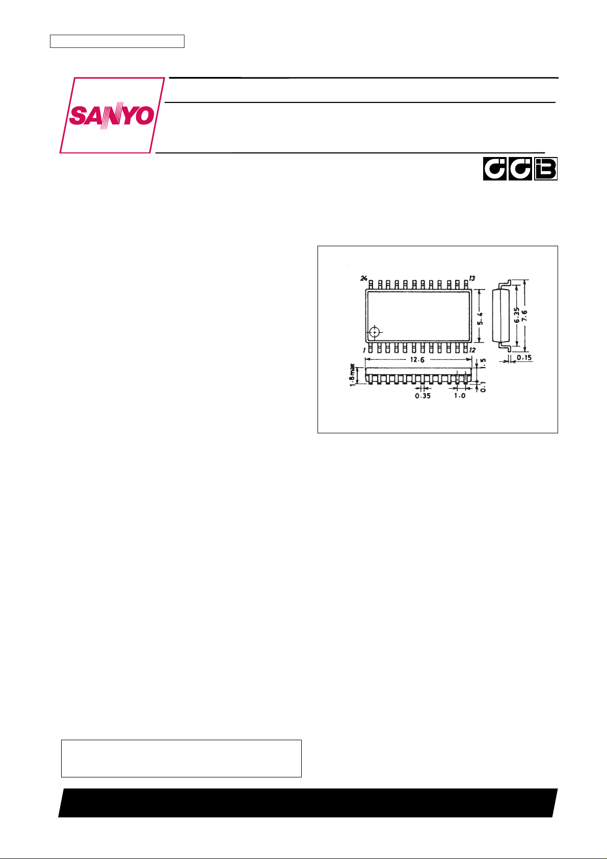
• Package: MFP24S
Package Dimensions
unit: mm
3112-MFP24S
SANYO: MFP24S
[LC72144M]
• CCB is a trademark of SANYO ELECTRIC CO., LTD.
• CCB is SANYO’s original bus format and all the bus
addresses are controlled by SANYO.
Page 2
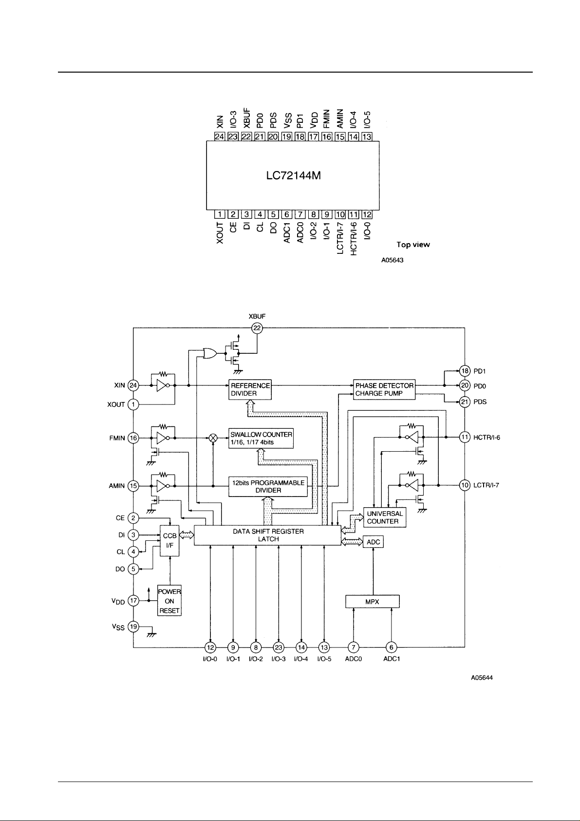
Pin Assignment
Block Diagram
No. 5377-2/22
LC72144M
Page 3
Specifications
Absolute Maximum Ratings at Ta = 25°C, VSS= 0 V
Note: A capacitor of at least 2000 pF must be inserted between the power supply, VDD, and VSS.
Allowable Operating Ranges at Ta = –40 to 85°C, VSS= 0 V
Note: 1. Period measurement
2. Refer to the item on the structure of the programmable divider.
3. Serial data: CTC = 0
4. Serial data: CTC = 1
No. 5377-3/22
LC72144M
Parameter Symbol Conditions Ratings Unit
Supply voltage V
DD
max V
DD
–0.3 to +7.0 V
V
IN
1 max CE, CL, DI –0.3 to +7.0 V
Maximum input voltage V
IN
2 max
XIN, FMIN, AMIN, HCTR/I-6, LCTR/I-7, I/O-0, I/O-4, I/O-5,
–0.3 to VDD+ 0.3 V
ADC0, ADC1
V
IN
3 max I/O-1 to I/O-3 –0.3 to +15 V
V
O
1 max DO –0.3 to +7.0 V
Maximum output voltage V
O
2 max XOUT, I/O-0, I/O-4, I/O-5, PD0, PD1, PDS, XBUF –0.3 to VDD+ 0.3 V
V
O
3 max I/O-1 to I/O-3 –0.3 to +15 V
I
O
1 max I/O-0, I/O-4, I/O-5, XBUF 0 to 3.0 mA
Maximum output current I
O
2 max DO 0 to 6.0 mA
I
O
3 max I/O-1 to I/O-3 0 to 10 mA
Allowable power dissipation Pd max Ta ≤85°C 220 mW
Operating temperature Topr –40 to +85 °C
Storage temperature Tstg –55 to +125 °C
Parameter Symbol Conditions min typ max Unit
Supply voltage
V
DD
1 V
DD
4.5 5.5
V
V
DD
2 VDD: Serial data hold voltage 2.0
V
IH
1 CE, CL, DI, I/O-1 to I/O-3 2.2 6.5 V
Input high-level voltage V
IH
2 I/O-0, I/O-4, I/O-5, HCTR/I-6, LCTR/I-7 2.2 V
DD
V
V
IH
3 LCTR/I-7: Pulse waveform, *1 2.2 V
DD
V
Input low-level voltage
V
IL
1 CE, CL, DI, I/O-0 to I/O-5, HCTR/I-6, LCTR/I-7 0 0.8 V
V
IL
2 LCTR/I-7: Pulse waveform, *1 0 0.8 V
Output voltage
V
O
1 DO 0 6.5 V
V
O
2 I/O-1 to I/O-3 0 13 V
f
IN
1 XIN: Sine wave, capacitor coupled 1.0 8.0 MHz
f
IN
2 FMIN: Sine wave, capacitor coupled 10 160 MHz
Input frequency
f
IN
3 AMIN: Sine wave, capacitor coupled 0.5 40 MHz
f
IN
4 HCTR/I-6: Sine wave, capacitor coupled 0.4 25 MHz
f
IN
5 LCTR/I-7: Sine wave, capacitor coupled 10 500 kHz
f
IN
6 LCTR/I-7: Pulse waveform, DC coupled, *1 4.0 20 × 10
3
Hz
Guaranteed crystal
Xtal1 XIN, XOUT: CI ≤ 120 Ω 4.0 7.0 MHz
oscillator ranges
Xtal2 XIN, XOUT: CI ≤ 50 Ω 7.1 10.5 MHz
V
IN
1 XIN 200 1500 mVrms
V
IN
2-1 FMIN: 10 ≤ f < 130 MHz, *2 40 1500 mVrms
V
IN
2-2 FMIN: 130 ≤ f < 160 MHz, *2 70 1500 mVrms
V
IN
3-1 AMIN: 2 ≤ f < 25 MHz, *2 40 1500 mVrms
V
IN
3-2 AMIN: 25 ≤ f < 40 MHz, *2 70 1500 mVrms
Input amplitudes
V
IN
3-3 AMIN: 0.5 ≤ f < 2.5 MHz, *2 40 1500 mVrms
V
IN
3-4 AMIN: 2.5 ≤ f ≤ 10 MHz, *2 70 1500 mVrms
V
IN
4-1 HCTR/I-6: 0.4 ≤ f ≤ 25 MHz, *3 40 1500 mVrms
V
IN
4-2 HCTR/I-6: 8 ≤ f ≤ 12 MHz, *4 70 1500 mVrms
V
IN
5-1 LCTR/I-7: 10 ≤ f < 400 kHz, *3 40 1500 mVrms
V
IN
5-2 LCTR/I-7: 400 ≤ f < 500 kHz, *3 20 1500 mVrms
V
IN
5-3 LCTR/I-7: 400 ≤ f < 500 kHz, *4 70 1500 mVrms
Input voltage range V
IN
6 ADC0, ADC1 0 V
DD
V
Continued on next page.
Page 4
Continued from preceding page.
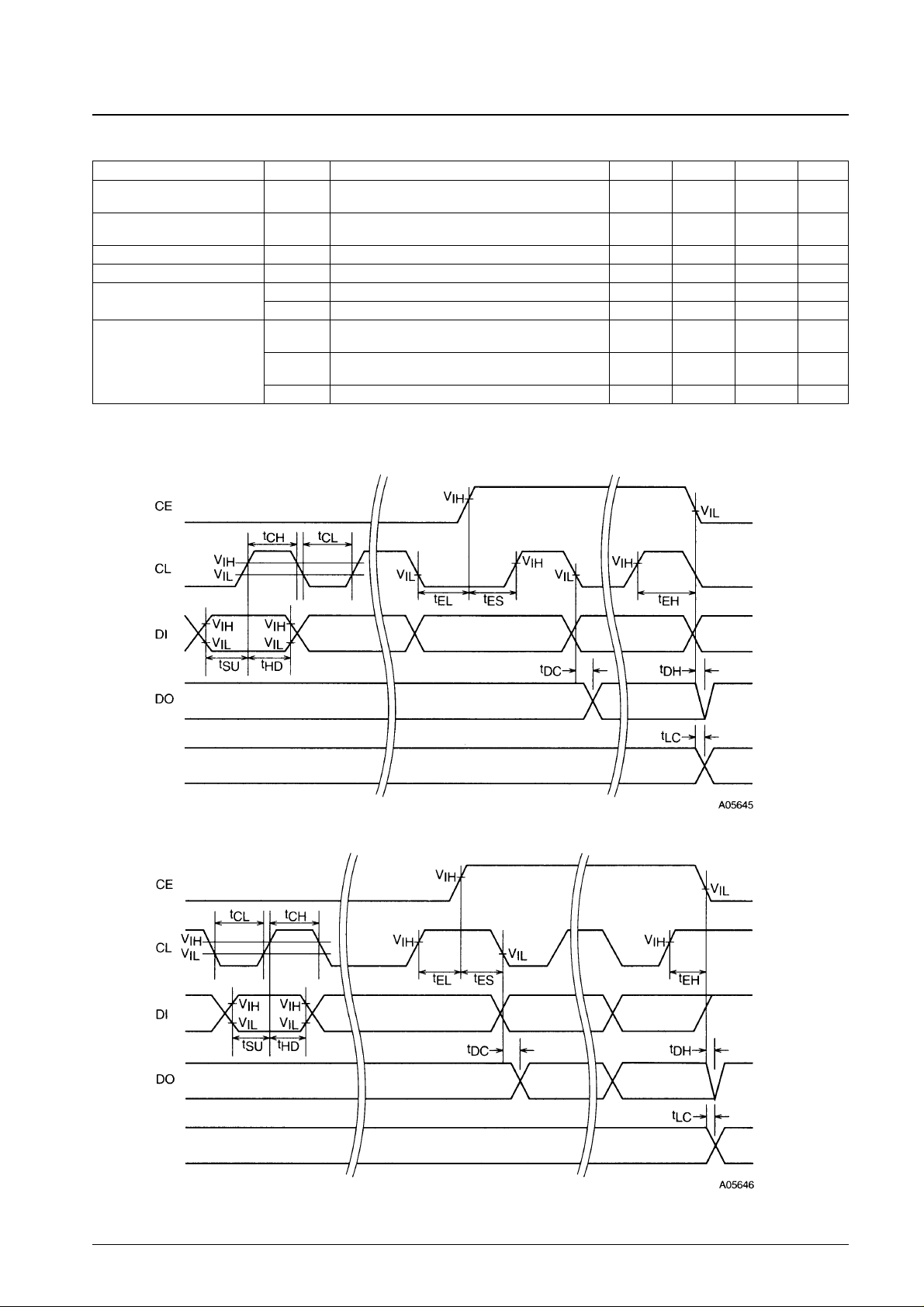
Note: Refer to the serial data timing.
Electrical Characteristics for the Allowable Operating Ranges
No. 5377-4/22
LC72144M
Parameter Symbol Conditions min typ max Unit
Data setup time t
SU
DI, CL: *1 0.45 µs
Data hold time t
HD
DI, CL: *1 0.45 µs
Clock low-level time t
CL
CL: *1 0.45 µs
Clock high-level time t
CH
CL: *1 0.45 µs
CE wait time t
EL
CE, CL: *1 0.45 µs
CE setup time t
ES
CE, CL: *1 0.45 µs
CE hold time t
EH
CE, CL: *1 0.45 µs
Data latch change time t
LC
*1 0.45 µs
t
DC
DO, CL
Differs depending on the values of
0.2 µs
Data output time the pull-up resistor and the printed circuit
t
DH
DO, CE
board capacitances. *1
0.2 µs
Parameter Symbol Conditions min typ max Unit
R
f
1 XIN 1.0 MΩ
R
f
2 FMIN 500 kΩ
Built-in feedback resistors R
f
3 AMIN 500 kΩ
R
f
4 HCTR/I-6 250 kΩ
R
f
5 LCTR/I-7 250 kΩ
Hysteresis V
HIS
CE, CL, DI, LCTR/I-7 0.1 V
DD
V
I
O
= –0.5 mA VDD– 0.5 V
High-level output voltage
V
OH
1 PD0, PD1, PDS, I/O-0, I/O-4, I/O-5 IO= –1 mA VDD– 1.0 V
I
O
= –2 mA VDD– 2.0 V
V
OH
2 XBUF IO= –0.5 mA VDD– 1.5 V
I
O
= 0.5 mA 0.5 V
V
OL
1 PD0, PD1, PDS, I/O-0, I/O-4, I/O-5 IO= 1 mA 1.0 V
I
O
= 2 mA 2.0 V
V
OL
2 XBUF IO= 0.5 mA 1.5 V
Low-level output voltage I
O
= 1 mA 0.2 V
V
OL
3 I/O-1 to I/O-3
I
O
= 2.5 mA 0.5 V
I
O
= 5 mA 1.0 V
I
O
= 9 mA 1.8 V
V
OL
4 DO: IO= 5 mA 1.0 V
I
IH
1 CE, CL, DI: VI= 6.5 V 5.0 µA
I
IH
2 I/O-1 to I/O-3: VI= 13 V 5.0 µA
I
IH
3
I/O-0, I/O-4, I/O-5, ADC0, ADC1, HCTR/I-6, LCTR/I-7:
5.0 µA
High-level input current V
I
= V
DD
IIH4 XIN: VI= V
DD
2.0 11 µA
I
IH
5 FMIN, AMIN: VI= V
DD
4.0 22 µA
I
IH
6 HCTR/I-6, LCTR/I-7: VI= V
DD
8.0 44 µA
I
IL
1 CE, CL, DI: VI= 0 V 5.0 µA
I
IL
2 I/O-0, to I/O-3: VI= 0 V 5.0 µA
I
IL
3
I/O-0, I/O-4, I/O-5, ADC0, ADC1, HCTR/I-6, LCTR/I-7:
5.0 µA
Low-level input current V
I
= 0 V
I
IL
4 XIN: VI= 0 V 2.0 11 µA
I
IL
5 FMIN, AMIN: VI= 0 V 4.0 22 µA
I
IL
6 HCTR/I-6, LCTR/I-7: VI= 0 V 8.0 44 µA
Output off leakage current
I
OFF
1 I/O-1 to I/O-3: VO= 13 V 5.0 µA
I
OFF
2 DO: VO= 6.5 V 5.0 µA
Continued on next page.
Page 5
Continued from preceding page.
Serial Data Timing
When CL is stopped at the low level
When CL is stopped at the high level
No. 5377-5/22
LC72144M
Parameter Symbol Conditions min typ max Unit
High-level 3-state off
I
OFFH
PD0, PD1, PDS: VO= V
DD
0.01 200 nA
leakage current
Low-level 3-state off
I
OFFL
PD0, PD1, PDS: VO= 0 V 0.01 200 nA
leakage current
Input capacitance C
IN
FMIN 6 pF
A/D converter linearity error Err ADC0, ADC1 –0.5 +0.5 LSB
Pull-down transistor on resistance
Rpd1 FMIN 80 200 600 kΩ
Rpd2 AMIN 80 200 600 kΩ
I
DD
1
V
DD
: Xtal = 10.35 MHz, fIN2 = 160 MHz,
10 15 mA
V
IN
2 = 70 mVrms, fIN4 = 25 MHz, VIN4 = 40 mVrms
Current drain
I
DD
2
V
DD
: PLL block stopped (PLL INHIBIT),
0.5 1.5 mA
Xtal oscillator operating (Xtal = 10.35 MHz)
I
DD
3 VDD: PLL block stopped, Xtal oscillator stopped 10 µA
Internal
data
latching
Old
Internal
data
latching
Old
New
New
Page 6
Pin Functions
No. 5377-6/22
LC72144M
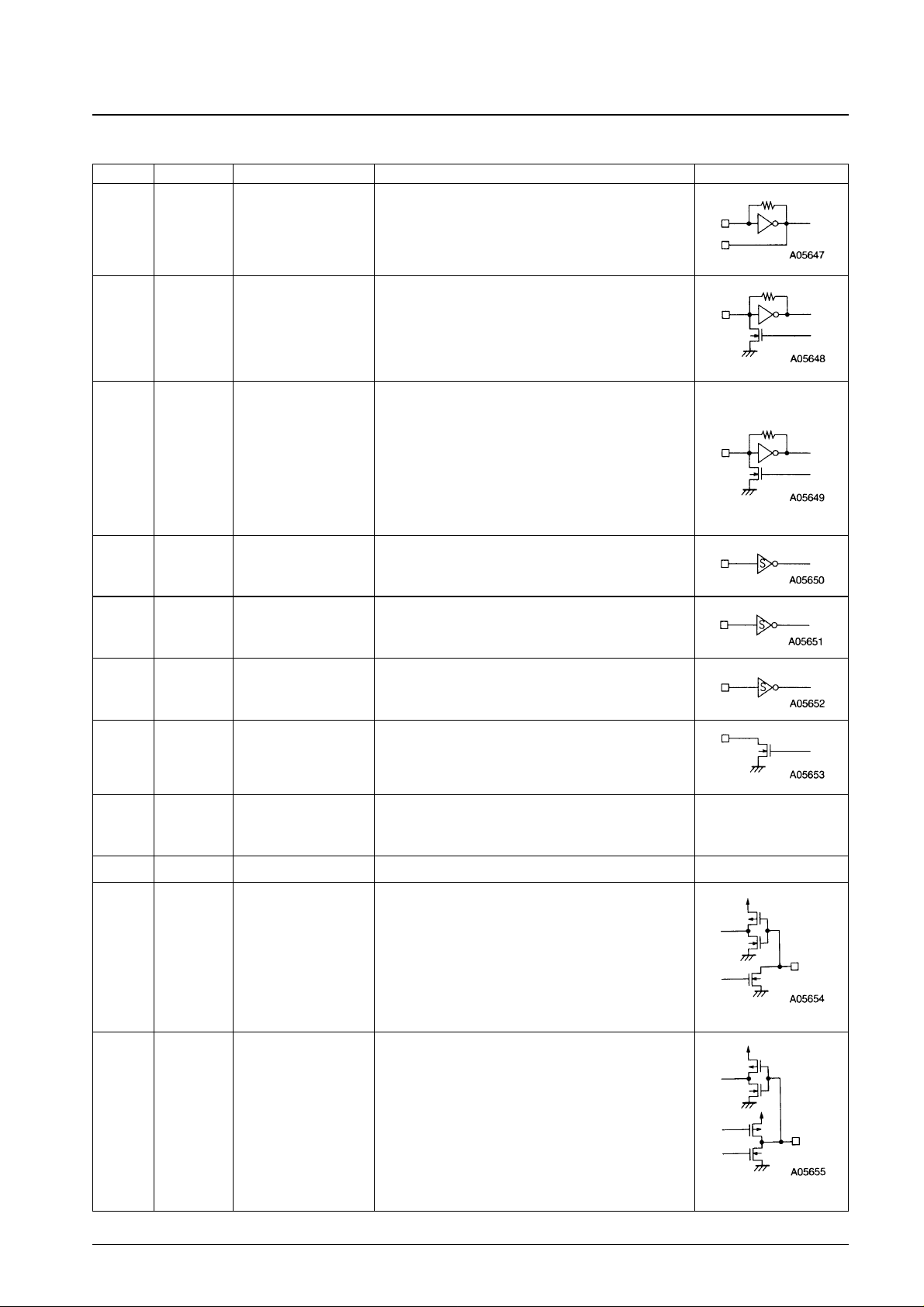
Pin No. Symbol Type Function Pin circuit
24
1
16
15
2
4
3
5
17
19
9
8
23
12
14
13
XIN
XOUT
FMIN
AMIN
CE
CL
DI
DO
V
DD
V
SS
I/O-1
I/O-2
I/O-3
I/O-0
I/O-4
I/O-5
Xtal oscillator
Local oscillator
signal input
Local oscillator
signal input
Chip enable
Clock
Input data
Output data
Power supply
Ground
General-purpose
I/O ports
General-purpose
I/O ports
Crystal oscillator connection
(4.5, 7.2, 10.25, or 10.35 MHz)
FMIN is selected when DVS in the serial data input is set to 1.
The input frequency range is 10 to 160 MHz.
The signal is transmitted to the swallow counter.
The divisor can be set to a value in the range 272 to 65,535.
AMIN is selected when DVS in the serial data input is set to 0.
When SNS in the serial data input is set to 1:
• The input frequency range is 2 to 40 MHz.
• The signal is transmitted to the swallow counter.
• The divisor can be set to a value in the range 272 to 65,535.
When SNS in the serial data input is set to 0:
• The input frequency range is 0.5 to 10 MHz.
• The signal is transmitted to the 12-bit programmable divider.
• The divisor can be set to a value in the range 4 to 4,095.
This pin must be set high during serial data input (DI) to the
LC72144M, or during serial data output (DO).
Used for data synchronization during serial data input (DI) to
the LC72144M, or during serial data output (DO).
Used to input serial data transferred to the LC72144M from the
controller.
Used to output serial data transferred the controller from the
LC72144M.
The LC72144M power supply connection. Provide a voltage
between 4.5 and 5.5 V when the PLL circuit is in operation.
The power on reset circuit operates when power is first applied.
—
The LC72144M ground connection. —
General-purpose I/O ports
The output circuits are open-drain circuits.
I/O-1 and I/O-2 are set to be input ports after the power on
reset. I/O-3 becomes an output port fixed at the low level.
These pins are switched between input and output by the I/O-1
to I/O-3 bits in the serial data transferred from the controller.
General-purpose I/O ports
The output circuits are complementary circuits.
These ports are set to be input ports after the power on reset.
These pins are switched between input and output by the I/O-0,
I/O-4, and I/O-5 bits in the serial data transferred from the
controller.
Continued on next page.
Page 7
Continued from preceding page.
No. 5377-7/22
LC72144M
Pin No. Symbol Type Function Pin circuit
7
6
21
18
20
11
10
22
ADC0
ADC1
PD0
PD1
PDS
HCTR/I-6
LCTR/I-7
XBUF
A/D converter input
Main charge pump output
Sub-charge pump output
General-purpose counter
General-purpose counter
Xtal oscillator buffer
A/D converter inputs
6-bit successive-approximation A/D converter
See the item on the structure of the A/D converter for details.
PLL charge pump output
A high level is output from the PD0 pin when the frequency
created by dividing the local oscillator frequency by N is higher
than the reference frequency. A low level is output when the
frequency is lower. The pin goes to the high-impedance state
when the frequencies agree.
The PD1 pin operates in the same manner.
A high-speed lockup circuit can be formed by using this pin in
combination with the main charge pump.
See the item on the structure of the charge pump for details.
HCTR is selected when the CTS1 bit in the serial data is set to 1.
• The input frequency range is 0.4 to 25 MHz.
• The signal passes through a divide-by-2 circuit and then is
input to a general-purpose counter. An integrating count can
also be performed.
• The result of the count is output from the MSB of the generalpurpose counter through the DO output pin.
• See the item on the structure of the general-purpose counter
for details.
When the serial data H/I-6 bit is set to 0:
• This pin functions as an input port, and its state is output from
the DO output pin.
LCTR is selected when the CTS1 bit in the serial data is set to 0.
When the CTS0 bit in the serial data is set to 1:
• The circuit switches to frequency measurement mode.
• The input frequency range is 10 to 500 kHz.
• The signal is input directly to the general-purpose counter
without passing through the divide-by-2 counter.
• The result of the count is output from the MSB of the generalpurpose counter through the DO output pin.
When the CTS0 bit in the serial data is set to 0:
• The circuit switches to period measurement mode.
• The input frequency range is 4 Hz to 20 kHz.
• The measurement period can be set to be 1 or 2 periods.
• The result of the count is output from the MSB of the generalpurpose counter through the DO output pin.
• See the item on the structure of the general-purpose counter
for details.
When the L/I-7 bit in the serial data is set to 0.
• This pin functions as an input port, and its state is output from
the DO output pin.
Output buffer for the crystal oscillator circuit.
If the XB bit in the serial data is set to 1, the output buffer
operates and the crystal oscillator signal (a pulse waveform) is
output.
If XB is 0, this pin outputs a low level. (Since XB is set to 0 after
the power on reset, the output will be fixed at the low level.)
Page 8

Serial Data Input and Output Methods
Data is input and output using the CCB (computer control bus) format, which is Sanyo's audio LSI serial bus format.
1. Serial data input (IN1/IN2)
2. Serial data output (OUT)
Note: 1. Since the DO pin is an n-channel open drain output, the data value transition time will differ depending on
the value of the pull-up resistor and the printed circuit board capacitance values.
Note: 2. The DO pin is normally open.
No. 5377-8/22
LC72144M
I/O mode
Address
Function
B0 B1 B2 B3 A0 A1 A2 A3
(1)
(2)
(3)
IN1
IN2
OUT
0 0 0 1 0 1 0 0
1 0 0 1 0 1 0 0
0 1 0 1 0 1 0 0
• Control data input mode (serial data input)
• 32 bits of data are input.
• Control data input mode (serial data input)
• 32 bits of data are input.
• Data output mode (serial data output)
• A number of bits equal to the number of clock cycles is
output.
The I/O mode is determined.
Internal
data
*1
*2
*2
Page 9

Structure of the DI Control Data
1. IN1
2. IN2
No. 5377-9/22
LC72144M
Address
Address
Page 10

Control Data Functions
No. 5377-10/22
LC72144M
No.
Control section/
Function Related data
data
Programmable
divider data
P0 to P15,
DVS, SNS
Sub-charge
pump
control data
PDC0, PDC1
Reference
divider data
R0 to R3
(1)
(2)
(3)
UL0, UL1, DLC
Data that sets the programmable divider’s divisor. It is a binary value and P15 is the MSB. The LSB
differs depending on the DVS and SNS bits. (
✕: don’t care)
Note: When P4 is the LSB, P0 to P3 are ignored.
These bits select the signal input pin (FMIN or AMIN) for the programmable divider and switch the input
frequency range.
Note: See the “Programmable Divider Structure” item for details.
Data that controls the sub-change pump
Note: The sub-charge pump can form a high-speed lockup circuit when combined with the PD0 and
PD1 pins (the main charge pump).
See the item on the structure of the charge pump for details.
Data that selects the reference frequency (fref)
Note: 1. Cannot be used when the crystal oscillator frequency is 10.25 or 10.35 MHz.
Note: 2. Cannot be used when the crystal oscillator frequency is 10.25 MHz.
Note: 3. PLL inhibit (backup mode)
The programmable divider block is stopped and FMIN and AMIN are both pulled down to
ground. The charge pump output goes to the floating state.
DVS SNS LSB Divisor setting (N)
1 ✕ P0 272 to 65535
0 1 P0 272 to 65535
0 0 P4 4 to 4095
DVS SNS Input port Input frequency range (MHz)
1 ✕ FMIN 10 to 160
0 1 AMIN 2 to 40
0 0 AMIN 0.5 to 10
PDC1 PDC0 Sub-charge pump state
0 ✕ High impedance
1 0 Charge pump operates (when unlocked)
1 1 Charge pump operates (normal operation)
R3 R2 R1 R0 Reference frequency (kHz)
0 0 0 0 100
*1
0 0 0 1 50
0 0 1 0 25
0 0 1 1 25
0 1 0 0 12.5
0 1 0 1 6.25
0 1 1 0 3.125
0 1 1 1 3.125
1 0 0 0 10
1 0 0 1 9
*2
1 0 1 0 5
1 0 1 1 1
1 1 0 0 3
*2
1 1 0 1 30
*2
1 1 1 0 *3, PLL inhibited and crystal oscillator stopped
1 1 1 1 *3, PLL inhibited
Continued on next page.
Page 11

Continued from preceding page.
No. 5377-11/22
LC72144M
No.
Control section/
Function Related data
data
Control data for
the DO and
I/O-5 pins
ULD, DT0,
DT1, IL0, IL1
A/D converter
control data
ADS, ADI0,
ADI1
(4)
(5)
OUT5
I/O-1, I/O-2, I/O-5
Data that determines the DO and I/O-5 pin outputs
Note: end-AD: A/D converter conversion completion
end-UC: General-purpose counter conversion completion
Note: 1.
Note: 2. However, this pin becomes open if the I/O-1 and I/O-2 pins are specified to be output ports.
Note: 2. Invalid if the I/O-5 pin is specified to be an input port.
Note: Cannot be used when the crystal oscillator is stopped. (The DO pin will not change state.)
(Reference divider: When R3 = R2 = R1 = 1, and R0 = 0)
A/D converter conversion start data
ADS = 1: Resets and starts the A/D converter
= 0: Resets the A/D converter
If ADC0 and ADC1 are specified for AD input at the same time, conversions are performed in the order
ADC0 first, then ADC1.
See the item on the structure of the A/D converter for details.
ULD DT1 DT0 DO I/O-5
0 0 0 Low when unlocked
0 0 1 end-AD
OUT5 flag
*2
0 1 0 end-UC
0 1 1 IN
*1
1 0 0 Open
1 0 1 end-AD
Low when unlocked
*2
1 1 0 end-UC
1 1 1 IN
*1
ADI1 ADI0 AD input pin
1 1 Stopped
1 0 ADC0
0 1 ADC1
0 0 ADC0, ADC1
Continued on next page.
IL1 IL0 IN state
0 0 Open
0 1 I-1 (pin state)
1 0 I-2 (pin state)
1 1 DO goes low when I-1 changes.
Start CE: HighFinish
(I-1 charge)
Page 12

Continued from preceding page.
No. 5377-12/22
LC72144M
No.
Control section/
Function Related data
data
General-
purpose
counter control
data
CTS0, CTS1,
CTE, GT0, GT1
CTP, CTC
I/O port control
data
I/O-0 to I/O-5
Output port
data
OUT0 to OUT5
General-
purpose
counter input
control data
H/I-6, L/I-7
Unlock
detection data
UL0, UL1
(6)
(7)
(8)
(9)
(10)
H/I-6, L/I-7
OUT0 to OUT5, ULD
I/O-0 to I/O-5, ULD
CTS0, CTS1
ULD, DT0, DT1
Data that selects the input pin (HCTR or LCTR) for the general-purpose counter
Data that specifies the start of a general-purpose counter measurement operation
CTE = 1: Count start
= 0: Count reset
Data that determines the general-purpose counter measurement time (in frequency mode) and number
of periods (in period mode)
CTP = 0: The general-purpose counter input is pulled down at count reset time (when CTE = 0).
= 1: The wait time is shortened by not pulling down the general-purpose counter input count reset
time (when CTE = 0). However, immediately after CTP is set to 1, the system must wait until
the general-purpose counter input pin is biased before starting a count.
The input sensitivity is lowered by setting CTC to 1. (Sensitivity: 10 to 30 mVrms)
Data that specifies the input or output state of the I/O ports
Data value = 0: Input port
= 1: Output port
Note: I/O-0, I/O-1, I/O-2, I/O-4, and I/O-5 are set to function as input ports after the power on reset.
I/O-3 is set to function as an output port after the power on reset.
Data that determines the output values of output ports O-0 to O-5
Data value = 1: Open or high
= 0: Low
Note: This data is invalid when the corresponding port is specified to function as an input port or as an
unlock state output.
Data that sets the general-purpose counter pins to function as input ports
H/I-6 = 0: I-6 (input port)
= 1: HCTR (general-purpose counter)
L/I-7 = 0: I-7 (input port)
= 1: LCTR (general-purpose counter)
Data that selects the phase error (øE) detection width used for PLL lock state discrimination
If a phase error in excess of the øE detection width listed in the table below is detected, the system
considers a phase error to have occurred and the PLL to be in the unlocked state. The detection pin
(DO or I/O-5) is set low in the unlocked state.
CTS1 CTS0 Input pin Measurement mode
1 ✕ HCTR Frequency
0 1 LCTR Frequency
0 0 LCTR Period
UL1 UL0 øE detection width Detection pin output
0 0 Stopped Open
0 1 0 øE output
1 0 ±0.5 µs øE with 1 to 2 ms expansion
1 1 ±1.0 µs øE with 1 to 2 ms expansion
Frequency measurement mode
Period measurement
GT1 GT0
Measurement time
Wait time (ms)
mode
(ms)
CTP = 0 CTP = 1
0 0 4 3 to 4 1 to 2 1 period
0 1 8 3 to 4 1 to 2 1 period
1 0 32 7 to 8 1 to 2 2 periods
1 1 64 7 to 8 1 to 2 2 periods
Continued on next page.
Expansion
Unlock state output
1 to 2 ms
I/O-5
Page 13

Continued from preceding page.
No. 5377-13/22
LC72144M
No.
Control section/
Function Related data
data
Crystal
oscillator circuit
XS0, XS1, XB
Phase
comparator
control data
DZ0, DZ1
Charge pump
control data
DLC
LSI test data
TEST0, TEST1,
TEST2
(11)
(12)
(13)
(14)
R0 to R3
Data that selects the crystal oscillator element
Note: The 10.25 MHz setting is selected after the power on reset.
Data that controls the crystal oscillator element buffer output
XB = 0: Buffer output off (This mode is selected after the power on reset.)
= 1: Buffer output on
Note: Turn off the XBUF output in FM reception mode (PD0 pin used).
Data that controls the phase comparator dead band
Note: DZA is selected after power-on reset.
Data that forces the charge pump output to the low level (VSS level).
DLC = 1: Low level
= 0: Normal operation
Note: If a deadlock occurs due to the VCO oscillator being stopped by the VCO control voltage (V
tune
)
becoming 0, the deadlock can be resolved by setting the charge pump output to the low level and
then setting V
tune
to VCC.
This data is set to the normal operating mode state after the power on reset.
Data that controls LSI testing
This data must all be set to 0, i.e.:
TEST0 = 0
TEST1 = 0
TEST2 = 0
Note: All the test data is set to 0 after the power on reset.
XS1 XS0 Xtal OSC
0 0 4.5 MHz
0 1 7.2 MHz
1 0 10.25 MHz
1 1 10.35 MHz
DZ1 DZ0 Insensitive band (dead zone) mode
0 0 DZA
0 1 DZB
1 0 DZC
1 1 DZD
Page 14

Structure of the DO Output Data (Serial Data Output)
3. OUT
No. 5377-14/22
LC72144M
No.
Control section/
Function Related data
data
I/O port data
I0 to I7
General-
purpose
counter binary
data
C0 to C19
A/D converter
ADC0 data
AD00 to AD05
A/D converter
data
ADC1 data
AD10 to AD15
(1)
(2)
(3)
(4)
I/O-0 to I/O-5,
H/I-6, L/I-7
CTS0, CTS1, CTE
ADI0, ADI1, ADS
ADI0, ADI1, ADS
I/O port data: The I0 to I7 pins reflect the latched I/O-0 to I/O-7 I/O port pin states. Data is latched
when data output mode is entered.
The pin states are latched regardless of the input or output mode specification.
Pin state = high: 1, low: 0
Counter contents
Bits C0 to C19 are the latched contents of the 20-bit binary counter. C0 is the LSB.
C19: MSB
C0: LSB
The result of A/D conversion of the signal input to the ADC0 pin is latched and output from the AD00 to
AD05 pins
AD05: MSB
AD00: LSB
The result of A/D conversion of the signal input to the ADC1 pin is latched and output from the AD10 to
AD15 pins
AD15: MSB
AD10: LSB
Address
Data with a value of 0.
Page 15

Programmable Divider
Note: ✕ = don’t care
General-Purpose Counter
The LC72144M includes a general-purpose 20-bit binary counter whose value can be read out from the DO pin, MSB
first.
When using this counter for frequency measurement, one of four measurement times (4, 8, 32, or 64 ms) is selected by
GT0 and GT1. The frequency input to either the HCTR or the LCTR pin can be measured by determining the number of
pulses input to the counter during the measurement period.
This counter can be used to measure the period of the signal input to the LCTR pin by determining how many cycles of a
reference signal (900 kHz) are input to the counter during one or two periods of the LCTR pin signal.
No. 5377-15/22
LC72144M
DVS SNS Divisor setting (N) Input frequency range Input port
(A) 1 ✕ 272 to 65535 10 to 160 MHz FMIN
(B) 0 1 272 to 65535 2 to 40 MHz AMIN
(C) 0 0 4 to 4095 0.5 to 10 MHz AMIN
Minimum input sensitivity (f [MHz])
(A) FMIN
10 ≤ f< 130 130 ≤ f < 160
40 mVrms 70 mVrms
(B) AMIN
2 ≤ f < 25 25 ≤ f < 40
40 mVrms 70 mVrms
(C) AMIN
0.5 ≤ f < 2.5 2.5 ≤ f < 10
40 mVrms 70 mVrms
One period/two
periods extraction
Check signal: 900 kHz
Input signal
switching gate
General-purpose counter
(20-bit binary counter)
DO pin
C = FIF × GT
C = (1/T) ÷ check signal (900 kHz)
0 to 3 4 to 7 8 to 11 12 to 15 16 to 19
Page 16

Check Signal Frequency
Note: * CTC = 0: 40 mVrms
CTC = 1: 70 mVrms
However, the frequency ranges will be as follows when CTC is 1.
HCTR: 8 to 12 MHz, LCTR: 400 to 500 kHz
The CTC data is input sensitivity switching data, and the input sensitivity is degraded when CTC is set to 1.
—: Not stipulated (not included in device guarantee)
( ): Actual performance estimates (reference values)
The CTP data determines the state of the general-purpose counter input pin (HCTR/LCTR) when the general-purpose
counter is reset (CTE = 0).
CTP = 0: The general-purpose counter input pin is pulled down.
= 1: The wait time is shortened to 1 to 2 ms by not pulling down the general-purpose counter input pin.
If CTP is set to 1, is must be set to 1 at least 4 ms before a count start (CTE = 1) is issued.
CTP must be set to and left at 0 if the counter is not used.
IF Counter Operation
Before starting a count operation with the general-purpose counter, reset that counter by setting CTE to 0.
A general-purpose counter count operation is started by setting the CTE bit in the serial data to 1. Although the serial
data is loaded into the LC72144M internal registers by changing the level on the CE input pin from high to low, the
input to the HCTR or LCTR pin must be provided within the wait period that follows the point when CE goes low at the
latest.
Next, the count result in the general-purpose counter after the measurement completes must be read out in the period
when CTE is 1, since the general-purpose counter is reset when CTE is set to 0.
Also note that although the signal input to the LCTR pin is transmitted directly to the general-purpose counter, the signal
input to the HCTR pin is only transmitted to the general-purpose counter after first being divided by two internally. Thus
the value of the result in the general-purpose counter is 1/2 the actual frequency of the signal input to the HCTR pin.
No. 5377-16/22
LC72144M
CTS1 CTS0 Input pin Measurement mode Frequency range Input sensitivity
S1 1 ✕ HCTR Frequency 0.4 to 25.0 MHz 40 mVrms*
S2 0 1 LCTR Frequency 10 to 500 kHz 40 mVrms*
S3 0 0 LCTR Period 4.0 to 20 ×10
3
Hz (pulse)
HCTR: Minimum input sensitivity rating [f (MHz)] LCTR: Minimum input sensitivity rating [f (kHz)]
CTC 0.4 ≤ f < 8 8 ≤ f < 12 12 ≤ f < 25 10 ≤ f < 400 400 ≤ f < 500
0 (normal mode) 40 mVrms
40 mVrms
40 mVrms 40 mVrms
20 mVrms
(1 to 10 mVrms) (0.1 to 3 mVrms)
1 (degraded mode) —
70 mVrms
— —
70 mVrms
(30 to 40 mVrms) (10 to 15 mVrms)
10.35 MHz
Xtal OSC 4.5 MHz 7.2 MHz 10.25 MHz
fref = 30, 9, 3 kHz
fref: A frequency other than
3, 9, or 30 kHz
Check signal 900 kHz 900 kHz 1025 kHz 1030 kHz 1150 kHz
Frequency measurement mode
Period measurement
GT1 GT0
Measurement time
Wait time (ms)
mode
(ms)
CTP = 0 CTP = 1
0 0 4 3 to 4 1 to 2 1 period
0 1 8 3 to 4 1 to 2 1 period
1 0 32 7 to 8 1 to 2 2 periods
1 1 64 7 to 8 1 to 2 2 periods
Page 17

Integrating Count
Note: CTE: 0 → • General-purpose counter reset
1 →
• General-purpose counter start
• Restarts on a new 1 setting
In integrated count mode, the count value is accumulated in the general-purpose counter.
Care is required to handle counter overflow.
Counter values: 0
H
to FFFFFH(1,048,575)
To implement the integrating count operation leave CTE set to 1. When the serial data (IN1) is transmitted again, the general-purpose counter will
start to measure the input again and the result will be added to the count.
No. 5377-17/22
LC72144M
Frequency
measurement
time
Period
measurement
time
Measurement time
Check signal
One period
Signal input
2.2 V (min)
0.8 V (max)
Wait time
CTE = 1
data
At least 40 mVrms*
(during frequency
measurement)
Note: * CTC = 0: 40 mVrms
CTC = 1: 70 mVrms
(during period measurement)
Internal data
latch (CTE)
Generalpurpose
counter
(Integration)
Count complete
Count complete
CTE = 1* CTE = 1* CTE = 1*
Page 18

Structure of the A/D Converter
The A/D converter is a 6-bit successive-approximation converter with a conversion time of 0.56 ms. The full-scale input
level (for a data value of 3FH) is (63/96) × VDD.
No. 5377-18/22
LC72144M
ADI1 ADI0 Input pin
1 1 Illegal value
1 0 ADC0
0 1 ADC1
0 0 ADC0/ADC1
Register
Data with a value of 0.
Multiplexer
Comparator
Decoder
DO pin
Discrimination
circuit
Conversion
CE ADS = 1
Start of conversion
Completion of
conversion
T
WA1
: 0.08 to 0.11 ms
T
WA1
: 0.08 to 0.09 ms
TAD: 0.56 to 0.62 ms
Page 19

Charge Pump
When unlock is detected following a channel change, PDS (the sub-charge pump) operates. The value of R1 changes to
R1M // R1S (R1S ≈ 100 Ω), as shown in following figure, decreasing the low-pass filter time-constant and accelerating
PLL locking.
The unlock detection data UL1 must be set to 1. The unlock detection range will be set to ±0.5 µs or ±1 µ s. If a phase
difference in excess of these values is detected the circuit will go to the unlock state and the sub-charge pump will
operate. When the circuit approaches the lock state and the phase difference falls under the unlock detection range, the
sub-charge pump operation will stop, i.e., the sub-charge pump will go to the high impedance state.
No. 5377-19/22
LC72144M
PDC1 PDC0 PDS (sub-charge pump state)
0 ✕ High impedance
1 0 Charge pump operates (when unlocked)
1 1 Charge pump operates (normal operation)
DLC PD1, PD0, PDS
0 Normal operation
1 Forced to low
Pins DO and I/O-5
Page 20

Others
1. Notes on the phase comparator dead zone
Cases where the charge pump is in the ON/ON state require special care during system design since the charge pump
outputs correction pulses even when the PLL is locked and it is easy for the loop to become unstable.
The following problems may occur in the ON/ON state.
➀
Sidebands may be generated by reference frequency leakage.
②
Sidebands may be generated by low frequency leakage due to the correction pulse envelope.
The settings that have a dead zone (the OFF/OFF settings) provide good loop stability, but it is hard to achieve a
good C/N ratio with these settings. Inversely, the settings with no dead zone (the ON/ON settings) allow a high C/N
ratio to be achieved but it is hard to achieve good loop stability with these settings.
Therefore, it can be effective to select either the DZA or DZB setting, i.e., a setting which has no dead zone, when an
S/N ratio of between 90 and 100 dB or higher is required in FM mode, or when the AM stereo pilot margin needs to
be increased. However, in cases where such a high FM S/N ratio is not required and where an adequate AM stereo
pilot margin can be achieved or AM stereo is not used, either the DZC or DZD setting, i.e., a setting which has a
dead zone, should be selected.
Dead Zone Definition
The phase comparator compares fp with a reference frequency (fr) as shown in Figure 1. Figure 2 shows the
characteristics of an ideal phase comparator, which outputs an output voltage (A) that is proportional to the phase
difference ø. However, in an actual IC, a region (dead zone) in which minute phase differences cannot be detected
occurs due to internal circuit delays and other factors (B). To implement an end product with a high S/N ratio, the
dead zone should be as small as possible.
However, there are cases where a larger dead zone can make a popularly-priced model easier to use. This is because
it is possible for RF leakage from the mixer to the VCO to modulate the VCO in popularly-priced models when a
strong RF input is applied. When the dead zone is small an output that compensates for this problem is generated,
and this output may itself modulate the VCO and generate beating with the RF frequency.
No. 5377-20/22
LC72144M
DZ1 DZ0 Dead zone mode Charge pump Dead zone
0 0 DZA ON/ON – –0 s
0 1 DZB ON/ON –0 s
1 0 DZC OFF/OFF +0 s
1 1 DZD OFF/OFF + +0 s
Leakage
Figure 1 Figure 2
Page 21

2. Notes on the FMIN, AMIN, HCTR/I-6, and LCTR/I-7 Pins
The coupling capacitors must be placed as close to the pin as possible. A capacitance of about 100 pF is desirable. In
particular, only use capacitances of under 1000 pF with the HCTR/I-6, and LCTR/I-7 pins. Large capacitances will
increase the time required for the pin to reach the bias level and, depending on the relationship with the wait time,
may cause counting errors.
3. Notes on IF counting → SD must be used together with IF counting
When using the general-purpose counter for IF counting, always use the IF-IC SD (station detect) signal. The
microcontroller should first check for the presence of the SD signal, and then turn on the IF count buffer only if that
signal is present to perform an IF count. Techniques that use only an IF count to implement an autosearch function
are dangerous because they may stop at frequencies that do not have a station due to leakage from the IF count
buffer.
4. Using the DO pin
In modes other than data output mode, the DO pin is also used for counter completion, unlock detection, and for
checking for changes in the input pin.
The state of the input pin (I/O-1, I/O-2) can be input to the controller directly through the DO pin.
5 Notes on using XBUF
When the XBUF output is turned on (when AM up-conversion is used), since the XBUF signal leaks into adjacent
pins, the pins PD0 and I/O-3, which are adjacent to XBUF, must not be used for AM reception control. Use the PD1
pin for the AM reception charge pump. Turn off the XBUF output (by setting the XB data to 0) when using PD0 and
I/O-3 for FM reception control.
6 Power supply pins
To exclude noise, a capacitor of at least 2000 pF must be inserted between the power supply VDDand VSSlines.
Locate this capacitor as close to the chip's VDDand VSSpins as possible.
Pin States at Power On and Reset
F: Floating
L: Low
No. 5377-21/22
LC72144M
State
Power On
Reset
State
Power On
Reset
Page 22

No. 5377-22/22
LC72144M
Application System Example
This catalog provides information as of August, 1997. Specifications and information herein are subject to
change without notice.
■ No products described or contained herein are intended for use in surgical implants, life-support systems, aerospace
equipment, nuclear power control systems, vehicles, disaster/crime-prevention equipment and the like, the failure of
which may directly or indirectly cause injury, death or property loss.
■ Anyone purchasing any products described or contained herein for an above-mentioned use shall:
➀ Accept full responsibility and indemnify and defend SANYO ELECTRIC CO., LTD., its affiliates, subsidiaries and
distributors and all their officers and employees, jointly and severally, against any and all claims and litigation and all
damages, cost and expenses associated with such use:
② Not impose any responsibility for any fault or negligence which may be cited in any such claim or litigation on
SANYO ELECTRIC CO., LTD., its affiliates, subsidiaries and distributors or any of their officers and employees
jointly or severally.
■ Information (including circuit diagrams and circuit parameters) herein is for example only; it is not guaranteed for
volume production. SANYO believes information herein is accurate and reliable, but no guarantees are made or implied
regarding its use or any infringements of intellectual property rights or other rights of third parties.
1 st IF: 10.8 MHz
2 nd Mixer input: 10.35 MHz
2 nd IF: 450 kHz
 Loading...