

Page 1

CMOS IC
Ordering number : ENN6113A
D0199TH (OT) /O3099TH (OT) /D2598RM (OT)No. 6113-1/22
SANYO Electric Co.,Ltd. Semiconductor Company
TOKYO OFFICE Tokyo Bldg., 1-10, 1 Chome, Ueno, Taito-ku, TOKYO, 110-8534 JAPAN
PLL Frequency Synthesizer
for Portable Equipment Electronic Tuning
LC72122V
Overview
The LC72122V is a low-voltage (1.8 to 3.6 V) PLL
frequency synthesizer IC that allows portable TV
(VHF)/FM/AM tuners to be constructed easily.
Features
• High-speed programmable frequency divider
— FMIN: 10 to 250 MHz..Pulse swallower
(divide-by-two prescaler built in)
— AMIN: 2 to 40 MHz ......Pulse swallower
0.5 to 10 MHz ...Direct division
• IF counter
— IFIN: 0.4 to 12 MHz......For use as an AM/FM IF
counter
• Reference frequency
— Selectable from one of nine frequencies (crystal
oscillator: 75 kHz)
1, 2.5, 3, 5, 3.125, 6.25, 12.5, 15, and 25 kHz
• Phase comparator
— Supports dead zone control
— Built-in unlock detection circuit
— Built-in deadlock clear circuit
— Sub-charge pump for fast frequency locking
• Built-in MOS transistor for forming an active low-pass
filter
• I/O ports
— Dedicated output ports: 3
— I/O ports: 2
— Supports clock time base output
• Serial Data I/O
— Supports CCB format communication with the
system controller.
• Operating ranges
— Supply voltage: 1.8 to 3.6 V
— Operating temperature: –20 to +70°C
• Package
—SSOP20
Package Dimensions
unit: mm
3179A-SSOP20
Any and all SANYO products described or contained herein do not have specifications that can handle
applications that require extremely high levels of reliability, such as life-support systems, aircraft’s
control systems, or other applications whose failure can be reasonably expected to result in serious
physical and/or material damage. Consult with your SANYO representative nearest you before using
any SANYO products described or contained herein in such applications.
SANYO assumes no responsibility for equipment failures that result from using products at values that
exceed, even momentarily, rated values (such as maximum ratings, operating condition ranges, or other
parameters) listed in products specifications of any and all SANYO products described or contained
herein.
• CCB is a trademark of SANYO ELECTRIC CO., LTD.
• CCB is SANYO’s original bus format and all the bus
addresses are controlled by SANYO.
SANYO: SSOP20
[LC72122V]
20
110
6.7
11
4.4
1.6max
0.1
0.650.22 0.43
1.0
6.4
0.5
0.15
Page 2
No. 6113-2/22
LC72122V
Specifications
Absolute Maximum Ratings at Ta = 25°C, V
SSd
= V
SSa
= 0 V
Parameter Symbol Conditions Ratings Unit
Maximum supply voltage V
DD
max V
DD
–0.3 to +4.0 V
V
IN
1 max CE, CL, DI –0.3 to +7.0 V
Maximum input voltage V
IN
2 max XIN, FMIN, AMIN, IFIN, AIN –0.3 to VDD+ 0.3 V
V
IN
3 max IO1, IO2 –0.3 to +8 V
V
O
1 max DO –0.3 to +7.0 V
Maximum output voltage V
O
2 max XOUT, PD –0.3 to VDD+ 0.3 V
V
O
3 max BO1 to BO3,AOUT –0.3 to +15 V
V
O
4 max IO1, IO2 –0.3 to +8 V
Maximum output current I
O
max BO1 to BO3, IO1, IO2, DO, AOUT 0 to 6.0 mA
Allowable power dissipation Pd max Ta ≤ 70°C: SSOP20 150 mW
Operating temperature Topr –20 to +70 °C
Storage temperature Tstg –40 to +125 °C
Ratings
Parameter Symbol Conditions
min typ max
Unit
Supply voltage V
DD
V
DD
1.8 2.2 3.6 V
Input high-level voltage
V
IH
1 CE, CL, DI 0.7 V
DD
6.5 V
V
IH
2 IO1, IO2 0.7 V
DD
7V
Input low-level voltage V
IL
CE, CL, DI, IO1, IO2 0 0.3 V
DD
V
V
O
1 DO 0 6.5 V
Output voltage V
O
2 BO1 to BO3, AOUT 0 13 V
V
O
3 IO1, IO2 0 7 V
f
IN
1 XIN: VIN1 75 kHz
f
IN
2 FMIN: VIN2 10 250 MHz
Input frequency f
IN
3 AMIN: VIN3, SNS = 1 2 40 MHz
f
IN
4 AMIN: VIN4, SNS = 0 0.5 10 MHz
f
IN
5 IFIN: VIN5 0.4 12 MHz
V
IN
1 XIN: fIN1 200 600 mVrms
V
IN
2-1 FMIN: f = 10 to 50 MHz 50 600 mVrms
V
IN
2-2 FMIN: f = 50 to 250 MHz 40 600 mVrms
Input amplitude V
IN
3 AMIN: fIN3, SNS = 1 30 600 mVrms
V
IN
4 AMIN: fIN4, SNS = 0 30 600 mVrms
V
IN
5-1 IFIN: fIN5, IFS = 1 30 600 mVrms
V
IN
5-2 IFIN: fIN5, IFS = 0 70 600 mVrms
Guaranteed crystal
Xtal XIN, XOUT * 75 kHz
oscillator frequency
Allowable Operating Ranges at Ta = –20 to +70°C, V
SSd
= V
SSa
= 0 V
* Note : Recommended crystal oscillator CI value : CI ≤ 35 kΩ (for a 75kHz crystal )
The circuit constants for the crystal oscillator circuit depend on the crystal used, the printed sircuit board pattem, and other items. Therefore we
recommend consulting with the manfacturer of the crystal for evaluation and reliability.
The extremely high input impedance of the XIN pins means that applications must take the possibility of leakage into account.
Page 3
No. 6113-3/22
LC72122V
Electrical Characteristics within the allowable operating ranges
Ratings
Parameter Symbol Conditions
min typ max
Unit
Rf1 XIN 8.0 MΩ
Internal feedback resistors
Rf2 FMIN 500 kΩ
Rf3 AMIN 500 kΩ
Rf4 IFIN 500 kΩ
Internal pull-down resistors
Rpd1 FMIN 200 kΩ
Rpd2 AMIN 200 kΩ
Internal output resistor Rd XOUT 250 kΩ
Hysteresis V
HIS
CE, CL, DI, IO1, IO2 0.1 V
DD
V
V
OH
1 PD: IO= –1 mA VDD– 0.5 V
Output high-level voltage
V
OH
2
AIN (PDS) : I
O
= – 2 mA (VDD= 1.8 to 2.7 V) VDD– 0.5 V
AIN (PDS) : I
O
= – 4 mA (VDD= 2.7 to 3.6 V) VDD– 0.5 V
V
OL
1 PD: IO= 1 mA 0.5 V
V
OL
2
AIN (PDS) : I
O
= 2 mA (VDD= 1.8 to 2.7 V) 0.5 V
AIN (PDS) : I
O
= 4 mA (VDD= 2.7 to 3.6 V) 0.5 V
BO1 to BO3, IO1, IO2; I
O
= 1 mA 0.2 V
Output low-level voltage V
OL
3 BO1 to BO3, IO1, IO2; IO= 5 mA 1.0 V
BO1 to BO3, IO1, IO2; I
O
= 8 mA 1.6 V
V
OL
4
DO: I
O
= 1 mA 0.2 V
DO: I
O
= 5 mA 1.0 V
V
OL
5 AOUT, IO= 5 mA, AIN= 1.2 V 1.5 V
I
IH
1 CE, CL, DI: VI= 6.5 V 5.0 µA
I
IH
2 IO1, IO2: VI= 7 V 5.0 µA
Input high-level current
I
IH
3 XIN: VI= V
DD
0.11 0.45 1.3 µA
I
IH
4 FMIN, AMIN: VI= V
DD
1.8 7.2 22 µA
I
IH
5 IFIN: VI= V
DD
1.8 7.2 22 µA
I
IH
6 AIN: VI= V
DD
200 nA
I
IL
1 CE, CL, DI: VI= 0 V 5.0 µA
I
IL
2 IO1, IO2: VI= 0 V 5.0 µA
Input low-level current
I
IL
3 XIN: VI= 0 V 0.11 0.45 1.3 µA
I
IL
4 FMIN, AMIN: VI= 0 V 1.8 7.2 22 µA
I
IL
5 IFIN: VI= 0 V 1.8 7.2 22 µA
I
IL
6 AIN: VI= 0 V 200 nA
I
OFF
1 BO1 to BO3, AOUT: VO= 13 V 5.0 µA
Output off leakage current I
OFF
2 IO1, IO2: VO= 7 V 5.0 µA
I
OFF
3 DO: VO= 6.5 V 5.0 µA
High-level three-state off
I
OFFH
PD: VO= V
DD
0.01 200 nA
leakage current
Low-level three-state off
I
OFFL
PD: VO= 0 V 0.01 200 nA
leakage current
Input capacitance C
IN
FMIN 6pF
I
DD
1VDD: Xtal = 75 kHz, fIN2 = 250 MHz, VIN2 = 40 mVrms 4 10 mA
Supply current I
DD
2
V
DD
: PLL block stopped (PLL inhibit),
10 µA
Xtal oscillator operating (Xtal = 75 kHz)
IDD3VDD: PLL block stopped, Xtal oscillator stopped 10 µA
Page 4

No. 6113-4/22
LC72122V
Pin Assignment
Top view
Block Diagram
Page 5

No. 6113-5/22
LC72122V
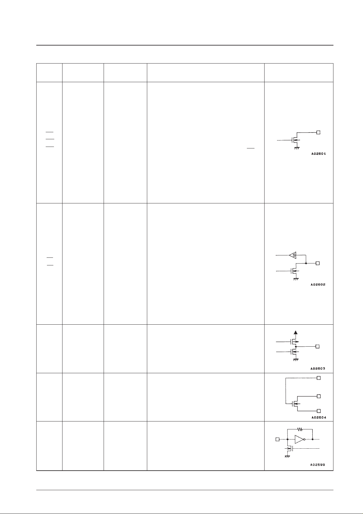
Pin Descriptions
Symbol Pin No. Type Functions Circuit configuration
19
20
12
11
1
3
2
4
13
14
XIN
XOUT
FMIN
AMIN
CE
CL
DI
DO
V
DD
V
SSd
Xtal
Local oscillator
signal input
Local oscillator
signal input
Chip enable
Clock
Input data
Output data
Power supply
Ground
• Crystal oscillator connections (75 kHz)
• FMIN is selected when the serial data input DVS bit is
set to 1.
• The input frequency range is from 10 to 250 MHz.
• The input signal passes through the internal divide-bytwo prescaler and is input to the swallow counter.
• The divisor can be in the range 272 to 65535. However,
since the signal has passed through the divide-by-two
prescaler, the actual divisor is twice the set value.
• AMIN is selected when the serial data input DVS bit is
set to 0.
• When the serial data input SNS bit is set to 1:
— The input frequency range is 2 to 40 MHz.
— The signal is directly input to the swallow counter.
— The divisor can be in the range 272 to 65535, and
the divisor used will be the value set.
• When the serial data input SNS bit is set to 0:
— The input frequency range is 0.5 to 10 MHz.
— The signal is directly input to a 12-bit programmable
divider.
— The divisor can be in the range 4 to 4095, and the
divisor used will be the value set.
• Set this pin high when inputting (DI) or outputting (DO)
serial data.
• Up to 6.5 V may be applied, regardless of the actual
supply voltage (VDD).
• Used as the synchronization clock when inputting (DI) or
outputting (DO) serial data.
• Up to 6.5 V may be applied, regardless of the actual
supply voltage (VDD).
• Inputs serial data transferred from the controller to the
LC72122V.
• Up to 6.5 V may be applied, regardless of the actual
supply voltage (VDD).
• Outputs serial data transferred from the LC72122V to
the controller. The data output is determined by the
DOC0 to DOC2 bits in the serial data.
• The LC72122V power supply pin. (V
DD
= 1.8 to 3.6 V)
• The power on reset circuit operates when power is first
applied.
• The LC72122V ground
Continued on next page.
Page 6
No. 6113-6/22
LC72122V
Continued from preceding page.
Symbol Pin No. Type Functions Circuit configuration
5
6
7
8
9
15
16
17
18
10
BO1
BO2
BO3
IO1
IO2
PD
AIN
AOUT
Vssa
Output ports
Input or output
ports
Charge pump
output
LPF amplifier
transistor
connections
IF counter
• Dedicated outputs
• The output states are determined by the BO1 to BO3
bits in the serial data.
Data: 0 = open, 1= low
• A time base signal (8 Hz) can be output from the BO1
pin. (When the serial data TBC bit is set to 1.)
• I/O dual-use pins
• The direction (input or output) is determined by bits IOC1
and IOC2 in the serial data.
Data: 0 = input port, 1 = output port
• When specified for use as input ports:
The state of the input pin is transmitted to the controller
over the DO pin.
Input state: low = 0 data value
high = 1 data value
• When specified for use as output ports:
The output states are determined by the IO1 and IO2
bits in the serial data.
Data: 0 = open, 1 = low
• These pins function as input pins following a power on
reset.
• PLL charge pump output
When the frequency generated by dividing the local
oscillator signal frequency by N is higher than the
reference frequency, a high level is output from the PD
pin. Similarly, when that frequency is lower, a low level is
output. The PD pin goes to the high-impedance state
when the frequencies match.
• The n-channel MOS transistor used for the PLL active
low-pass filter.
• The AIN pin is connected internally to a fast locking subcharge pump circuit (PDS).
• Vssa is special-purpose ground pin.
• Accepts an input in the frequency range 0.4 to 12 MHz.
• The input signal is directly transmitted to the IF counter.
• The result is output starting the MSB of the IF counter
using the DO pin.
• Four measurement periods are supported: 8, 16, 32, and
64 ms.
IFIN
Page 7

No. 6113-7/22
LC72122V
Serial Data I/O Procedures
The LC72122V inputs and outputs data using the Sanyo CCB (computer control bus) audio IC serial bus format. This IC
adopts an 8-bit address format CCB.
I/O mode
Address
Function
B0 B1 B2 B3 A0 A1 A2 A3
1
2
3
IN1 (82)
IN2 (92)
OUT (A2)
00010100
10010100
01010100
• Control data input mode (serial data input)
• 24 data bits are input.
• See the “DI Control Data (serial data input) Structure”
item for details on the meaning of the input data.
• Control data input mode (serial data input)
• 24 data bits are input.
• See the “DI Control Data (serial data input) Structure”
item for details on the meaning of the input data.
• Data output mode (serial data output)
• The number of bits output is equal to the number of clock
cycles.
• See the “DO Output Data (Serial Data Output) Structure”
item for details on the meaning of the output data.
Page 8

No. 6113-8/22
LC72122V
DI Control Data (serial data input) Structure
1. IN1 Mode
2. IN2 Mode
Page 9

No. 6113-9/22
LC72122V
DI Control Data Descriptions
No. Control block/data Description Related data
Programmable divider data • Data that sets the programmable divider
P0 to P15 A binary value in which P15 is the MSB. The LSB changes depending on DVS and SNS.
(*: Don’t care.)
Note: P0 to P3 are ignored when P4 is the LSB.
DVS, SNS • Selects the signal input pin (AMIN or FMIN) for the programmable divider, switches the
frequency range. (*: Don’t care.)
Note: See the “Programmable Divider” item for details.
Reference divider data • Reference frequency (fref) selection data
R0 to R3
Note: PLL INHIBIT
The programmable divider and IF counter blocks are stopped, the FMIN, AMIN,
and IFIN pins go to the pulled-down state, and the charge pump output pin goes to
the high-impedance state.
IF counter control data • IF counter measurement start specification
CTE CTE = 1: Counter start
CTE = 0: Counter reset
GT0, GT1 • IF counter measurement time determination
Note: See the “IF Counter Structure” item for details.
I/O port specification data • Data that specifies input or output for the I/O dual-use pins (IO1, IO2)
IOC1, IOC2 Data: 0 = input mode, 1 = output mode
Output port data • BO1 to BO3, IO1, and IO2 output state data
BO1 to BO3, IO1, IO2 Data: 0 = open, 1 = low
• “Data = 0: Open” is selected following a power-on reset.**
(1)
(2)
(3)
(4)
(5)
IFS
IOC1
IOC2
DVS SNS LSB Divisor setting (N) Actual divisor
1 * P0 272 to 65535 Twice the value of the setting
0 1 P0 272 to 65535 The value of the setting
0 0 P4 4 to 4095 The value of the setting
DVS SNS Input pin Input frequency range
1 * FMIN 10 to 250 MHz
0 1 AMIN 2 to 40 MHz
0 0 AMIN 0.5 to 10 MHz
GT1 GT0 Measurement time (ms) Wait time (ms)
0 0 8 3 to 4
0 1 16 3 to 4
1 0 32 7 to 8
1 1 64 7 to 8
R3 R2 R1 R0 Reference frequency (kHz)
0000 25
0001 25
0010 25
0011 25
0 1 0 0 12.5
0 1 0 1 6.25
0 1 1 0 3.125
0 1 1 1 3.125
1000 5
1001 5
1 0 1 0 2.5
1011 1
1100 3
1101 15
1 1 1 0 PLL INHIBIT + Xtal OSC STOP
1 1 1 1 PLL INHIBIT
Continued on next page.
Page 10

No. 6113-10/22
LC72122V
Continued from preceding page.
No. Control block/data Description Related data
DO pin control data • Data that determines DO pin output
DOC0, DOC1, DOC2
The open state is selected following a power-on reset.
Note: 1. end-UC: IF counter measurement completion check
➀ When end-UC is set and an IF count is started (CTE = 0 → 1), the DO pin
automatically goes to the open state.
➁ When the IF count measurement completes, the DO pin goes low and
the count completion check operation is enabled.
➂ The DO pin goes to the open state due to serial data I/O (CE: high).
2. Goes to the open state if the IO pin itself is set to be an output port.
Caution: The DO pin always goes to the open state during the data input period (during the
period when CE is high in mode IN1 or IN2), regardless of the values of the DO pin
control data (DOC0 to DOC2). Also, the DO pin outputs the content of the internal
DO serial data in synchronization with the CL pin signal during the data output period
(during the period when CE is high in the OUT mode) regardless of the values of
the DO pin control data (DOC0 to DOC2).
Unlock detection data • Selects the phase error (øE) detection range for PLL lock discrimination.
UL0, UL1 When a phase error greater than the specified range occurs, the LC72122V determines
that the PLL is unlocked. (*: Don’t care.)
Note: When unlocked, the DO pin goes low and the serial data output UL bit is 0.
Phase comparator • Phase comparator dead zone control data
control data
DZ0, DZ1
Dead zone width: DZA < DZB < DZC < DZD
Clock time base • An 8 Hz 40% duty clock time base signal can be output from BO1 by setting TBC to 1.
TBC (The BO1 data will be ignored.)
Charge pump control data • Data that forcibly controls the charge pump output
DLC
Note: The LC72122V provides a technique for escaping from deadlock by setting Vtune to
V
CC
(deadlock clear circuit). This is used when the circuit is deadlocked due to the
VCO oscillator being stopped by the VCO control voltage (Vtune) being 0 V.
(6)
(7)
(8)
(9)
(10)
UL0, UL1,
CTE,
IOC1, IOC2
DOC0,
DOC1,
DOC2
BO1
DOC2 DOC1 DOC0 DO pin state
0 0 0 Open
0 0 1 Low when the unlock state is detected
0 1 0 end-UC
*1
0 1 1 Open
1 0 0 Open
1 0 1 The IO1 pin state
*2
1 1 0 The IO2 pin state
*2
1 1 1 Open
UL1 UL0 øE detection width Detector output
0 0 Stopped Open
0 1 0 øE is output directly
1 * ±6.67 µs øE is extended by 1 to 2 ms
DZ1 DZ0 Dead zone mode
0 0 DZA
0 1 DZB
1 0 DZC
1 1 DZD
DLC Charge pump output
0 Normal operation
1 Forced low
Continued on next page.
Page 11

No. 6113-11/22
LC72122V
Continued from preceding page.
DO Output Data (Serial Data Output) Structure
3. OUT mode
DO Output Data
No. Control block/data Description Related data
IF counter control data • IFIN pin input sensitivity control data. This data should be set to 1 in normal operation.
(11) IFS Setting this data to 0 switches the LC72122V to a reduced input sensitivity mode in which
the sensitivity is reduced by 10 to 30 mVrms.
Sub-charge pump control • This data controls the sub-charge pump (PDS) which is provided for fast locking.
(12) data By setting SUBC to 1, applications can set the sub-charge pump circuit to the operating UL0, UL1
SUBC state and increase the speed of frequency looking.
IC test data • IC test data
TEST 0 to TEST2 TEST0
(13)
TEST1 All three bits must be set to 0.
TEST2
All the test data is set to 0 at a power-on reset.**
(14) DNC Data is set to 0
No. Control block/data Description Related data
I/O port data • Data latched from the states of the I/O ports, pins IO1 and IO2.
I2, I1 • This data reflects the pin states, regardless of whether they are in input or output mode.
• The data is latched when OUT mode is selected.
I1 ← IO1 pin state High: 1
I2 ← IO2 pin state Low: 0
PLL unlock data • Data latched from the state of the unlock detection circuit
UL UL ← 0: Unlocked
UL ← 1: Locked or in detection stopped mode
IF counter binary data • Data latched from the state of the IF counter, which is a 20-bit binary counter.
C19 to C0 C19 ← Binary counter MSB
C0 ← Binary counter LSB
(1)
(2)
(3)
IOC1,
IOC2
UL0,
UL1
CTE,
GT0,
GT1
*
Note: * Data with a value of “0”
**Note : Although the IC is initialized after power is first applied by the power on reset circuit, applications must also send a full set of data over the CCB bus
immediately after power is first applied to assure safe and stable operation.
Page 12

No. 6113-12/22
LC72122V
Serial Data Input (IN1/IN2) tSU, tHD, tEL, tES, tEH, ≥ 0.75 µs, tLC< 0.75 µs
1. CL: Normal high
2. CL: Normal low
Serial Data Output (OUT) tSU, tHD, tEL, tES, tEH, ≥ 0.75 µs, tDC, tDH< 0.35 µs
1. CL: Normal high
2. CL: Normal low
Note: Since the DO pin is an n-channel open drain circuit, the times for the data to change (tDCand tDH) will differ depending on the value of the pull-up
resistor, printed circuit board capacitance.
Page 13

No. 6113-13/22
LC72122V
Serial Data Timing
CL Stopped at the Low Level
CL Stopped at the High Level
Parameter Symbol Pins Conditions min typ max Unit
Data setup time t
SU
DI, CL 0.75 µs
Data hold time t
HD
DI, CL 0.75 µs
Clock low-level time t
CL
CL 0.75 µs
Clock high-level time t
CH
CL 0.75 µs
CE wait time t
EL
CE, CL 0.75 µs
CE setup time t
ES
CE, CL 0.75 µs
CE hold time t
EH
CE, CL 0.75 µs
Data latch change time t
LC
0.75 µs
Data output time
t
DC
DO, CL
These times depend on the pull-up resistance
0.35 µs
t
DH
DO, CE
and the printed circuit board capacitances.
0.35 µs
Page 14

No. 6113-14/22
LC72122V
Programmable Divider Structure
Note: * Don’t care.
Sample Programmable Divider Divisor Calculations
1. For a 50 kHz FM step size (DVS = 1, SNS = *: FMIN selected)
• FM RF = 90.0 MHz (IF = +10.7 MHz)
FM VCO = 100.7 MHz
PLL fref = 25 kHz (R0 to R1 = 1, R2 to R3 = 0)
100.7 MHz (FM VCO) ÷ 25 kHz (fref) ÷ 2 (FMIN: divide-by-two prescaler) = 2014 → 07DE (HEX)
2. For a 5 kHz SW step size (DVS = 0, SNS = 1: AMIN high-speed side selected)
• SW RF = 21.75 MHz (IF = +450 kHz)
SW VCO = 22.20 MHz
PLL fref = 5 kHz (R0 to R2 = 0, R3 = 1)
22.2 MHz (SW VCO) ÷ 5 kHz (fref) = 4440 → 1158 (HEX)
3. For a 9 kHz MW step size (DVS = 0, SNS = 0: AMIN low-speed side selected)
• MW RF = 1008 kHz (IF = +450 kHz)
MW VCO = 1458 kHz
PLL fref = 3 kHz (R0 to R1 = 0, R2 to R3 = 1)
1458 kHz (MW VCO) ÷ 3 kHz (fref) = 486 → 1E6 (HEX)
DVS SNS Input pin Set divisor Actual divisor: N Input frequency range (MHz)
A1* FMIN 272 to 65535 Twice the set value 10 to 250
B 0 1 AMIN 272 to 65535 The set value 2 to 40
C 0 0 AMIN 4 to 4095 The set value 0.5 to 10
Page 15

No. 6113-15/22
LC72122V
IF Counter Structure
The LC72122V IF counter is a 20-bit binary counter, and takes the IF signal from the IFIN pin as its input. The result of
the count can be read out serially, MSB first, from the DO pin.
The IF frequency (Fc) is measured by determining how many pulses were input to the IF counter in the stipulated
measurement time, GT.
Fc = (C = Fc × GT) C: count value (number of pulses)
Sample IF Counter Frequency Calculations
1. For a measurement time (GT) of 32 ms and a count value (C) of 53980 (hexadecimal), which is 342,400 (decimal)
IF frequency (Fc) = 342,400 ÷ 32 ms = 10.7 MHz
2. For a measurement time (GT) of 8 ms and a count value (C) of E10 (hexadecimal), which is 3600 (decimal)
IF frequency (Fc) = 3600 ÷ 8 ms = 450 kHz
C
GT
GT1 GT0
Measurement time
Measurement period (GT) (ms) Wait time (t
WU
) (ms)
0 0 8 3 to 4
0 1 16 3 to 4
1 0 32 7 to 8
1 1 64 7 to 8
Page 16

No. 6113-16/22
LC72122V
IF Counter Operation
Before starting the IF count, the IF counter must be reset in advance by setting CTE in the serial data to 0.
The IF count is started by changing the CTE bit in the serial data from 0 to 1. The serial data is latched by the LC72122V
when the CE pin is dropped from high to low. The IF signal must be supplied to the IFIN pin in the period between the
point the CE pin goes low and the end of the wait time at the latest. Next, the value of the IF count at the end of the
measurement period must be read out during the period CTE is 1. This is because the IF counter is reset when CTE is set
to 0.
Note: When operating the IF counter, the control microcontroller must first check the state of the IF-IC SD (station
detect) signal and only after determining that the SD signal is present turn on IF buffer output and execute an IF
count operation. Auto-search techniques that use only the IF counter are not recommended, since it is possible for
IF buffer leakage output to cause incorrect stops at points where there is no station.
If the auto-search technique is implemented using only the IF counter in combination with an IF-IC without SD
output, sensitivity-degradation mode ( IFS = 0 ) should be selected.
IFIN Minimum Sensitivity Ratings
f(MHz)
Note:Values in parentheses are actual performance values presented as reference data.
IFS 0.4 ≤ f < 0.5 0.5 ≤ f < 8 8 ≤ f ≤ 12
1: Normal mode
30mVrms
30mVrms
30mVrms
(0.1 to 3mVrms) (1 to 10mVrms)
0: Degradation mode
70mVrms
70mVrms
70mVrms
(5 to 15mVrms) (20 to 40mVrms)
Page 17

Unlock Detection Timing
1. Unlock Detection Determination Timing
Unlock detection is performed in the reference frequency (fref) period (interval). Therefore, in principle, unlock
determination requires a time longer than the period of the reference frequency. However, immediately after changing
the divisor N (frequency) unlock detection must be performed after waiting at least two periods of the reference
frequency.
No. 6113-17/22
LC72122V
Figure 1 Unlock Detection Timing
For example, if fref is 1 kHz (and thus the period is 1 ms), after changing the divisor N, the system must wait at least
2 ms before checking for the unlocked state.
Figure 2 Circuit Structure
Page 18

No. 6113-18/22
LC72122V
2. Unlock Detection Software
Figure 3
3. When Outputting Unlock Data Using Serial Data Output:
Once the LC72122V detects an unlocked state, it does not reset the unlock data (UL) until the next data output (or
data input) operation is performed. At the data output ① point in Figure 3, although the VCO frequency is stable
(locked), the unlock data remains set to the unlocked state since no data output has been performed since the value of
N was changed. Thus, even though the frequency became stable (locked), from the point of view of the data, the
circuit is in the unlocked state. Therefore, the data output ① immediately following a change to the value of N should
be seen as a dummy data, and the data from the second data output (data output ②) and later outputs should be seen
as valid data.
Lock Determination Flowchart
Page 19

No. 6113-19/22
LC72122V
When directly outputting data from the DO pin (set up by the DO pin control data)
Since the DO pin outputs the unlocked state (locked: high, unlocked: low) the timing considerations in the technique
described in the previous section are not necessary. After changing the value of N, the locked state can be determined
after waiting at least two periods of the reference frequency.
Notes on Clock Time Base Usage
When the clock time base output is used, the value of the pull-up resistor for the output pin (BO1) must be at least 100 kΩ.
We recommend the use of a Schmitt input on the receiving controller (microprocessor) to prevent chattering.This is to
avoid degradation of the VCO C/N characteristics when using the built-in low-pass filter transistor to form the loop
filter. Since the clock time base output pin and the low-pass filter transistor ground are the same mode in the IC, the time
base output pin current fluctuations must be suppressed to limit the influence on the low-pass filter.
Other Items
1. Notes on the Phase Comparator Dead Zone
Since correction pulses are output from the charge pump even if the PLL is locked when the charge pump is in the
ON/ON state, the loop can easily become unstable. This point requires special care when designing application
circuits. Since the characteristics may change with the supply voltage, an optimal dead zone must be selected for the
actual end product itself. The table shows the state when VDDis 2.2 V (typical). As the supply voltage increases, the
charge pump circuit tends to go to the ON/ON state.
The following problems may occur in the ON/ON state.
• Side band generation due to reference frequency leakage
• Side band generation due to both the correction pulse envelope and low frequency leakage
DZ1 DZ0 Dead-zone mode Charge pump Dead zone
0 0 DZA ON/ON – –0 s
0 1 DZB ON/ON –0 s
1 0 DZC OFF/OFF +0 s
1 1 DZD OFF/OFF + +0 s
Page 20

No. 6113-20/22
LC72122V
Schemes in which a dead zone is present (OFF/OFF) have good loop stability, but have the problem that acquiring a
high C/N ratio can be difficult. On the other hand, although it is easy to acquire a high C/N ratio with schemes in
which there is no dead zone, it is difficult to achieve high loop stability. Therefore, it can be effective to select DZA
or DZB, which have no dead zone, in applications which require an FM S/N ratio in excess of 90 to 100 dB, or in
which an increased AM stereo pilot margin is desired. On the other hand, we recommend selecting DZC or DZD,
which provide a dead zone, for applications which do not require such a high FM signal-to-noise ratio and in which
either AM stereo is not used or an adequate AM stereo pilot margin can be achieved.
Dead Zone
The phase comparator compares fp to a reference frequency (fr) as shown in Figure 4. Although the characteristics of
this circuit (see Figure 5) are such that the output voltage is proportional to the phase difference ø (line A), a region
(the dead zone) in which it is not possible to compare small phase differences occurs in actual ICs due to internal
circuit delays and other factors (line B). A dead zone as small as possible is desirable for products that must provide
a high S/N ratio.
However, since a larger dead zone makes this circuit easier to use, a larger dead zone is appropriate for popularlypriced products. This is because it is possible for RF signals to leak from the mixer to the VCO and modulate the
VCO in popularly-priced products in the presence of strong RF inputs. When the dead zone is narrow, the circuit
outputs correction pulses and this output can further modulate the VCO and generate beat frequencies with the RF
signal.
Figure 4
Figure 5
2. Notes on the FMIN, AMIN, and IFIN Pins
Coupling capacitors must be placed as close as possible to their respective pin. A capacitance of about 100 pF is
desirable. In particular, if a capacitance of 1000 pF or over is used for the IF pin, the time to reach the bias level will
increase and incorrect counting may occur due to the relationship with the wait time.
3. Notes on IF Counting → SD must be used in conjunction with the IF counting time
When using IF counting, always implement IF counting by having the microprocessor determine the presence of the
IF-IC SD (station detect) signal and turn on the IF counter buffer only if the SD signal is present. Schemes in which
auto-searches are performed with only IF counting are not recommended, since they can stop at points where there is
no signal due to leakage output from the IF counter buffer.
Page 21

No. 6113-21/22
LC72122V
4. DO Pin Usage Techniques
In addition to data output mode times, the DO pin can also be used to check for IF counter count completion and for
unlock detection output. Also, an input pin state can be output unchanged through the DO pin and input to the
controller.
5. Power Supply Pins
A capacitor must be inserted between the power supply VDDand VSSpins for noise exclusion. This capacitor must
be placed as close as possible to the VDDand VSSpins.
6. Note on VCO designing
VCO ( local oscillator ) must keep its oscillation even if the control voltage ( Vtune ) goes to 0V. When there is a
possibility of oscillation halt, Vtune must be forcibly set to VCCtemporarily to prevent the PLL from being
deadlocked. ( Deadlock clear circuit )
7. Structure of the sub-charge pump circuit provided for high-speed frequency locking
The fast locking sub-charge pump circuit (PDS) is controlled by the SUBC control signal.
When the PDS circuit is operating, the effective resistance of R1 is reduced to about 250 Ω.
This reduces the locking time.
Note that during normal reception, SUBC should be set to 0 to stop PDS circuit operation, and SUBC should be set
to 1 to operate the PDS circuit when changing stations.
Pin States at a Power-On Reset
Note: Although the IC is initialized after power is first applied by the power on reset circuit, applications must also send a full set of data over the CCB bus
immediately after power is first applied to assure safe and stable operation.
Page 22

PS. No. 6113-22/22
LC72122V
This catalog provides information as of December, 1999. Specifications and information herein are
subject to change without notice.
Specifications of any and all SANYO products described or contained herein stipulate the performance,
characteristics, and functions of the described products in the independent state, and are not guarantees
of the performance, characteristics, and functions of the described products as mounted in the customer’s
products or equipment. To verify symptoms and states that cannot be evaluated in an independent device,
the customer should always evaluate and test devices mounted in the customer’s products or equipment.
SANYO Electric Co., Ltd. strives to supply high-quality high-reliability products. However, any and all
semiconductor products fail with some probability. It is possible that these probabilistic failures could
give rise to accidents or events that could endanger human lives, that could give rise to smoke or fire,
or that could cause damage to other property. When designing equipment, adopt safety measures so
that these kinds of accidents or events cannot occur. Such measures include but are not limited to protective
circuits and error prevention circuits for safe design, redundant design, and structural design.
In the event that any or all SANYO products (including technical data, services) described or contained
herein are controlled under any of applicable local export control laws and regulations, such products must
not be exported without obtaining the export license from the authorities concerned in accordance with the
above law.
No part of this publication may be reproduced or transmitted in any form or by any means, electronic or
mechanical, including photocopying and recording, or any information storage or retrieval system,
or otherwise, without the prior written permission of SANYO Electric Co., Ltd.
Any and all information described or contained herein are subject to change without notice due to
product/technology improvement, etc. When designing equipment, refer to the “Delivery Specification”
for the SANYO product that you intend to use.
Information (including circuit diagrams and circuit parameters) herein is for example only; it is not
guaranteed for volume production. SANYO believes information herein is accurate and reliable, but
no guarantees are made or implied regarding its use or any infringements of intellectual property rights
or other rights of third parties.
Sample Application System
This section is susceptible to noise due to its high
impedance. Therefore, the pattern lines should be kept
as short as possible and this area should be covered
with a ground pattern.
 Loading...