

Page 1
Ordering number : ENN*6830
LC680100A
32-Bit RISC Microcontroller
Preliminary
Overview
The LC680100A is a 32 bit microcontroller developed exclusively by Sanyo, based on a 32 bit RISC CPU and
incorporating on a single chip a high speed multiplier, 2kB of cache RAM, 2kB data RAM, DRAM control unit, external
memory control unit and peripheral
It is an ideal control device for digital cameras, color printers and hand held data terminals.
Features
(1) CPU core :32 bit RISC (Speed: 15MHz, Instruction cycle time: 67ns)
(2) High Speed Multiplier :16bit x 16bit (in 1 instruction cycle)
(3) Instruction cache RAM :2kB (512x32bit)
(4) Data RAM :2kB (512x32bit)
(5) DRAM Control Unit
(6) External memory bus control unit
(7) I/O port :One 16 bit I/O port, one 8 bit I/O port
(8) UART :Two full duplex asynchronous channels (one channel has 16bit FIFO)
(9) Serial I/O :One three-wire synchronous clock, 8 bit
(10) Timer :4 channels (TM0 = 16bit + 16bit)
(TM1, TM2, TM 3 = 8bit + 8bit)
(11) PWM Output :Three 8 bit resolution outputs (Common with TM1, TM2, TM3)
(12) Interrupt controller :13 source events (5 internal, 8 external), 5 vectored
(13) OSC circuit :Two types: main and RC. VCO/PLL is built-in, frequency multiplication possible.
(14) Standby :Standby (HOLD) and sleep (HALT) modes available
(15) VDD :3.3V typ.
Package and Pins
SQFP100, 10 0 pins
Development tools
A C compiler, assembler and emulator are available to be run on a PC.
CMOS IC
Ver.1.2
D0798
N3000 RM (IM) IT No.6830-1/16
Page 2
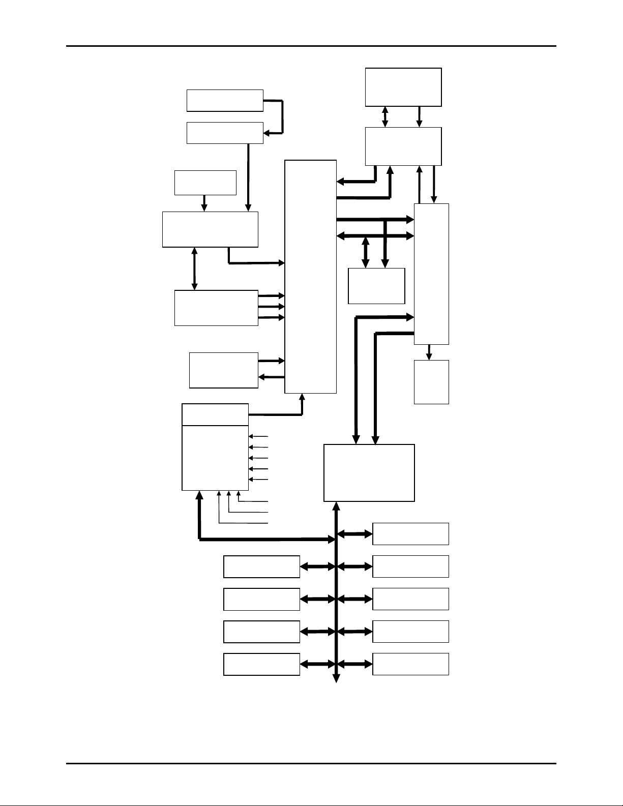
System Bl ock Diagram
LC680100A
Main OSC
Multiplie r Circu it
RC OSC
System Clock, Standby
Control
Mode Control
Reset Control
Coprocessor
(Multiplier)
32bit
RISC
CORE
Instruction Cache
(2k bytes)
Instruction Cache
Control
Data RAM
(2k bytes)
Bus
Control
DRAM
Control
Interrupt Control
Interrupt en ab le
control
TM0H
TM0L
TM1H
TM2H
TM3H
SIO0
UART0
UART1
Timer 0
Timer 1
Timer 2
Timer 3
Figure 1 LC680100A System Block Diagram
Special Function R eg ister
SFR Bus Control
SIO0
UART0
UART1
Port 0
Port 1
No.6830-2/16
Page 3
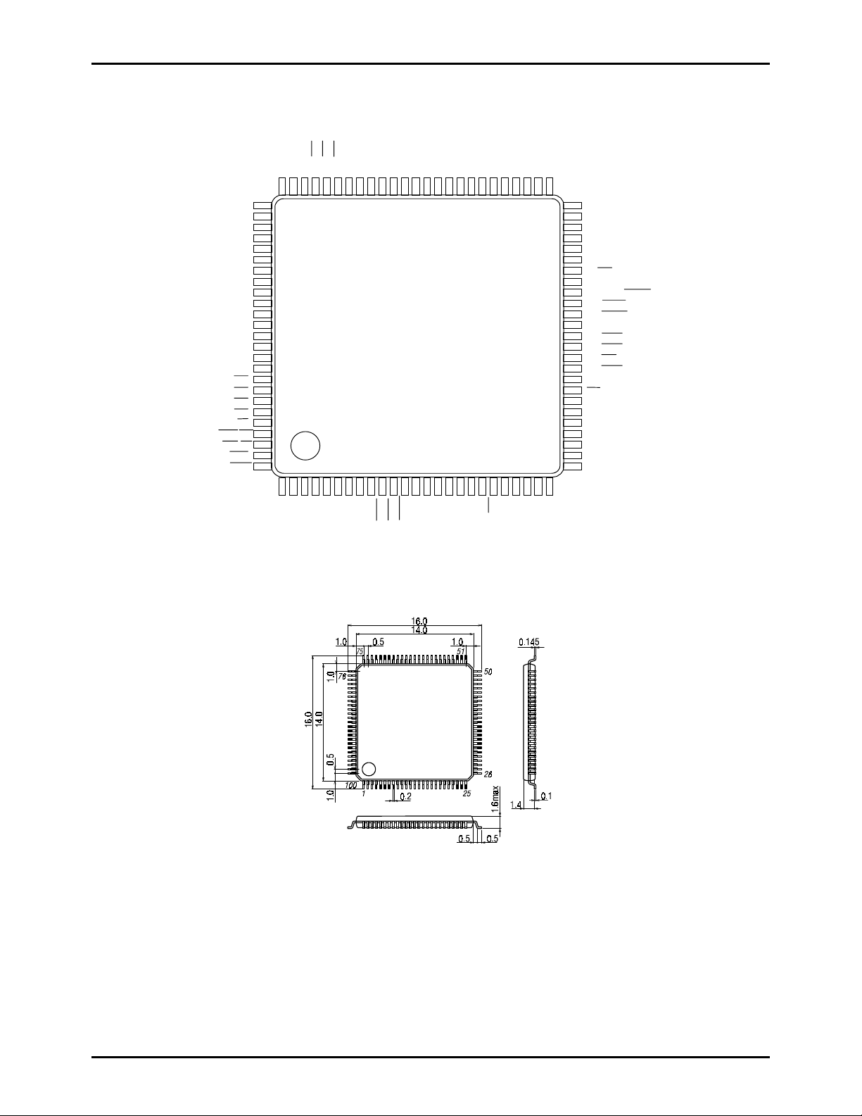
Terminal Assignment Diagram
(SQFP100, 0. 5 mm pit c h)
VSS
D0
D1
LC680100A
VDD
A27/CS3
A22
A23
A25/CS5
A17
A18
A19
A20
A21
A24
A26/CS4
A13
A11
A12
A14
A15
A16
A7
A8
A9
A10
VDD
D10
D11
D12
D13
D14
D15
VSS
CS0
CS1
CS2
CS6
WRU/UBS
WRL/WR
WAIT
BREQ
Package Dimension
(unit : mm)
3181B
D2
76
D3
77
D4
78
D5
79
D6
80
D7
81
82
D8
83
D9
84
85
86
87
88
89
90
91
92
93
94
95
RD
96
97
98
99
100
1 2 3 4 5 6 7 8 910111213141516171819202122232425
VDD
CK1
LC680100A
VSS
VDD
CK2
CMP
VSS
CKOT
CKIN
HOLDI
RESET
PHIOT
MODE
TEST
57 56 55 54 53 52 5160 59 5867 66 65 64 63 6270 69 68 6175 74 73 72 71
VDD
P02/SDO
P03/SDI
P00/TXD0
P04/SCK
P01/RXD0
VSS
P05/PWM0
P06/PWM1
P07/T0IN/INT0
50
49
48
47
46
45
44
43
42
41
40
39
38
37
36
35
34
33
32
31
30
29
28
27
26
P08/INT1
A6
A5
A4
A3
A2
A1
A0/LBS
VSS
P17/MCLK/HOLDO
P16/IRQOT
P15/RFREQ
P14/DMXS
P13/CASL
P12/CASU
P11/RAS
P10/BGNT
VDD
NMI
P0F
P0E
P0D/RXD1
P0C/TXD1
P0B/PWM2
P0A/INT3
P09/INT2
SANYO : SQFP-100
No.6830-3/16
Page 4
LC680100A
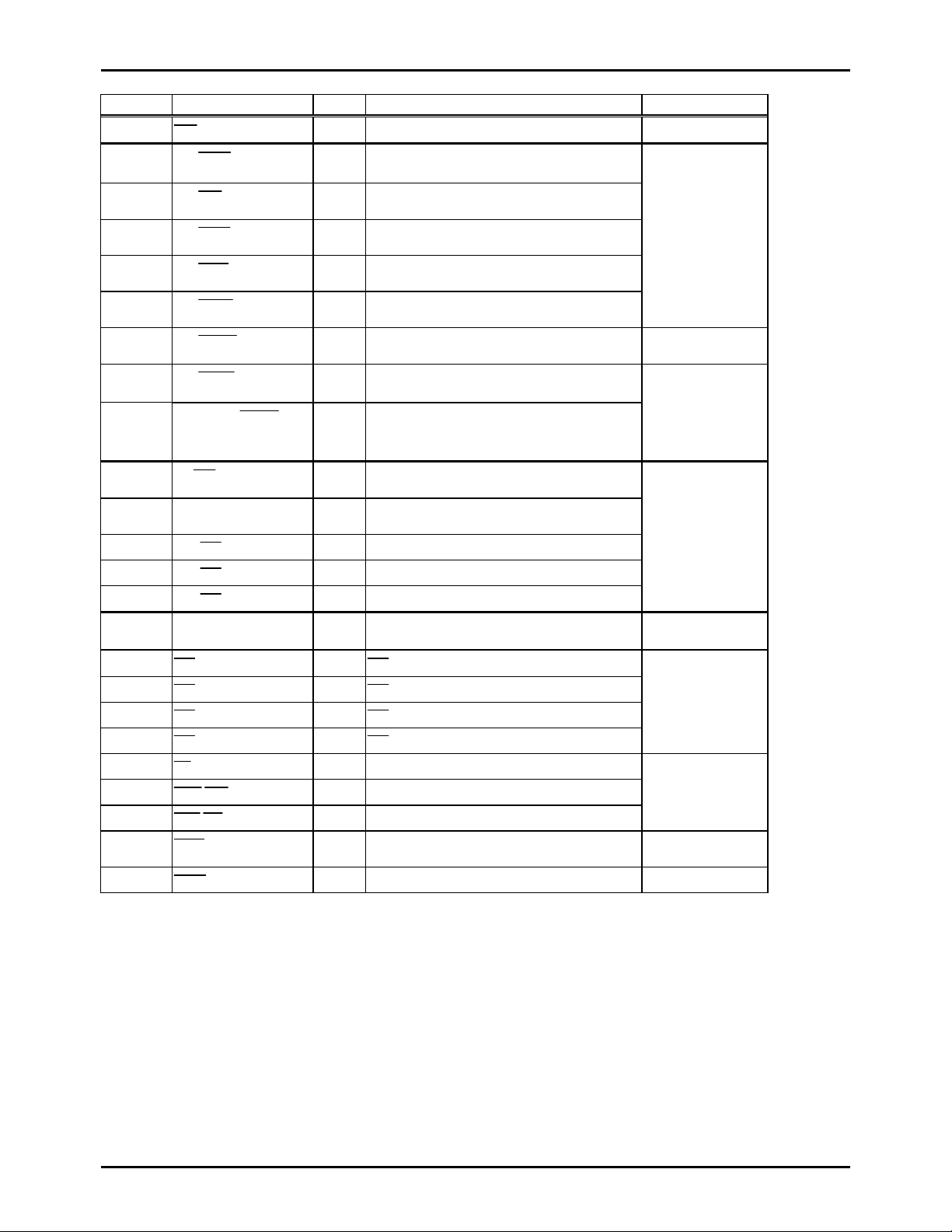
Terminal Functions
Pin Number Pin Name I/O Function Description Pin Format
1,6,15,34,55
,82
4,9,24,43,73
,91
2 CK1 I Input to main oscillator Schmitt Input
3 CK2 O Output from main oscillat or CMOS output
5 CMP I/O Phase comparator filter pin (multiplier circuit). Schmitt Input•Tristate
7 CKOT O CK1 or half frequency clock output from multiplier CMOS output
8 CKIN I External clock input Schmitt Input
10
11
12
13 MODE I Bus mode setting at reset Schmitt Input
14 TEST I Test input (Normally connected to VSS) Schmitt Input
16 P00/TXD0 I/O PORT0 bit0 I/O.
17 P01/RXD0 I/O PORT0 bit1 I/O.
18 P02/SDO I/O PORT0 bit2 I/O.
19 P03/SDI I/O PORT0 bit3 I/O.
20
21 P05/PWM0 I/O PORT0 bit5 I/O.
22 P06/PWM1 I/O PORT0 bit6 I/O.
23 P07/T0IN/INT0 I/O PORT0 bit7 I/O.
25 P08/INT1 I/O PORT0 bit8 I/O.
26 P09/INT2 I/O PORT0 bit9 I/O.
27 P0A/INT3 I/O PORT0 bit10 I/O.
28 P0B/PWM2 I/O PORT0 bit11 I/O.
29 P0C/TXD1 I/O PORT0 bit12 I/O.
30 P0D/RXD1 I/O PORT0 bit13 I/O.
31 P0E I/O PORT0 bit14 I/O.
32
VDD - Power supply +ve -
VSS - Power supply -ve -
PHIOT
HOLDI
RESET
SCK
P04/
P0F I/O PORT0 bit15 I/O.
Note: PU = pull-up
output
O System clock output CMOS output
I HOLD request input Schmitt Input
I Reset terminal Schmitt Input
•Used as input:
Also UA R T0 send
Also UART0 receive
Also SIO0 data out
Also SIO0 data in
I/O PORT0 bit4 I/O.
Also SIO0 clock
Also PWM0 output
Also PWM1 output
Timer0 event input
INT0 input
INT1 input
INT2 input
INT3 input
PWM2 output
UART1 send
UART1 receive
Schmitt Input;
presence of PU
resistor software
selectable.
•Used as Output:
CMOS/N-ch OD
mode so ftware
selectable.
No.6830-4/16
Page 5
LC680100A
Pin Number Pin Name I/O Function Description Pin Format
33
35
36
37
38
39
40
41
42
44
45 to 54,
56 to 69
70
71
72
74 to 81,
83 to 90
92
93
94
95
96
97
98
99
100
NMI
BGNT
P10/
P11/
P12/
P13/
P14/
P15/
P16/
P17/MCLK/
A0/
RAS
CASU
CASL
DMXS
RFREQ
IRQOT
LBS
HOLD0
A1to A24 I/O Bus Address bit1 to 24.
CS5
A25/
A26/
A27/
CS4
CS3
D0 to D15 I/O Bus data bit0 to 15 Schmitt Input•Tristate
CS0
CS1
CS2
CS6
RD
WRU/UBS
WRL/WR
WAIT
BREQ
I NMI interrupt Schmitt Input
I/O PORT1 bit0 input.
Also bus grant output.
Schmitt Input•Tristate
output
I/O PORT1 bit1 input. Also
DRAM control R AS signal out.
I/O PORT1 bit2 input. Also
DRAM control C ASU signal out.
I/O PORT1 bit3 input. Also
DRAM control C ASL signal out.
I/O PORT1 bit4 input. Also
DRAM contr ol DM XS signal out.
I/O PORT1 bit5 input. Also
DRAM control RFREQ I/O.
I/O PORT1 bit6 input.
Also IRQOT output.
Schmitt Input•PU
Output
Schmitt Input•Tristate
output
I/O PORT1 bit7 input.
MCLK output,
HOLD sta te output
I/O Bus Address bit0 or
Lower byte strobe signal.
I/O
Bus Address bit25 or CS5.
I/O
Bus Address bit26 or CS4
I/O
Bus Address bit27 or CS3.
Schmitt Input•Tristate
output
output
I/O
CS0
I/O
CS1
I/O
CS2
I/O
CS6
I/O Bus read signal.
I/O Upper byte write signal or Upper byte strobe.
Schmitt Input•Tristate
output
Schmitt Input•Tristate
output
I/O Upper byte write signal or Write.
I/O Bus cycle wait Schmitt Input•PU
output
I Bus request. Schmitt Input
No.6830-5/16
Page 6

LC680100A
1. Absolute Maximum Ratings at Ta = 25°C, VSS = 0V
Parameter Symbol
Supply voltage VDDmax
Input voltage VI(1)
Output voltage VO(1)
Input/Output volt a ge VIO(1)
High level peak
output current
High level total output
current
Low level peak output
current
Low level total output
current
Maximum power
consumption
Operating temperature
range
Storage temperature
range
IOPH(1) Each output pin Current at each pin -5 mA
IOAH(1) P00 to P08 Total of 9 pins -80 mA
∑
IOAH(2) P09 to P0F Total of 7 pins -80 mA
∑
IOPL(1) Each output pin Current at each pin 20 mA
IOAL(1) P00 to P07 Total of 8 pins 80 mA
∑
IOAL(2) P08 to P0F Total of 8 pins 80 mA
∑
Pdmax
Topg -20 to +70
Tstg -55 to +125
Pins Conditions Ratings
VDD
Note1
Pins for each
input only
Pins for each
output only
Pins for both
input and output
SQFP100
Note2
-0.3 to +4.6
-0.3 to VDD+0.3
-0.3 to VDD+0.3
-0.3 to VDD+0.3
Ta = -20 to 70°C 440 mW
Note1:All VDD terminals (pin1, 6, 15, 34, 55, 82) should be connected externally.
All VSS terminals (pin4, 9, 24, 43, 73, 91) should be connected externally.
Note2:Reflow method is recommended when soldering the SQFP package.
V
V
V
V
°
°
C
C
Unit
No.6830-6/16
Page 7

LC680100A
2. Recommended Operating Rang e at Ta = -20 to 70°C, VSS = 0V
Parameter Symbol Pins Conditions
Operating supply
voltage range
Supply voltage
(Memory hold)
High level input
voltage
Low level input
voltage
Operation cycle time
External system clock
frequency
External clock pul se
width
External clock risi ng
and falling time
Operation frequency
range
VDD (1) VDD 3.0 3.3 3.6 V
Keep RAM and
VHD VDD
VIH(1)
VIH(2) CK1 0.7VDD VDD
VIL(1)
VIL(2) CK1 VSS 0.3VDD
tCYC(1) CKIN 300K to 15MHz 66 3333
tCYC(2) CK1
fEXCKIN CKIN Figure 1 300k 15M
fEXCK1 CK1 Figure 1 400k 15M
tCKINL
tCKINH
tCK1L
tCK1H
tEXR
tEXF
fCK1 CK1, CK2 Figure 2, Table 1 400k 8M Hz
Input pins
except CK1
Input pins
except CK1
CKIN Figure 1 28
CK1 Figure 1 28
CKIN, CK1 Figure 1 5
Register data in
Standby mode.
0.7VDD VDD
VSS 0.3VDD
400K to 15MHz
(VCO is not
used.)
Ratings
Min. Typ. Max.
2.5 3.6 V
132 5000
Unit
V
V
ns
Hz
ns
ns
No.6830-7/16
Page 8

LC680100A
3. Electrical Characteristics at Ta = -20 to 70°C, VSS = 0V, VDD = 3.0 to 3.6V
Parameter Symbol Pins Conditions
Pins for each input
only
Pins for both input
and output
Pins for each input
only
RFREQ,WAIT
Input/output
commonly terminals
except written above
Port0 with PU option,
RFREQ
P15/
VIN = VDD 5
VIN = VDD
Output disabled
VIN = VSS -5
VIN = VSS
Output disabled
VIN = VSS
Output disabled
IOH = -0.05mA VDD-0.5
Input/output
commonly terminals
except written above,
PHIOT
CKOT,
Pins for each ou tput
only
Pins for both input
and output
Port0 with PU option,
RFREQ
P15/
Each input only, I/O
terminal
NMI
2
INT0 to INT3
RESET
Figure 4 2 ms
IOH = -1mA VDD-0.5
IOL = 4mA 0.4
IOL = 4mA 0.4
1K 20K
0.1
Figure 4
High level input
current
Low level input
current
High level output
voltage
Low level output
voltage
PU resistor
Hysterisis voltage
External interrupt
pulse width
Reset input pulse
width
IIH(1)
IIH(2)
IIL(1)
IIL(2) P15/
IIL(3)
VOH(1)
VOH(2)
VOL(1)
VOL(2)
rPU
vHIS
tINTL
tINTH
tRESL
VCO frequency fVCO CKOT Figure 5 4M 16M Hz
VCO lock-up time
RC oscillation
frequency
Ceramic oscillation
stabilizing time
Current consumption
in run mode
Current consumption
in sleep mode
Current consumption
in standby mode
tLOCK CMP,CKOT
fRC
Built-in RC oscillation
circuit
tCF CK1,CK2 Figure 3 10 ms
IDDRUN VDD CKIN=15MHz 60 120 mA
IDDSLP VDD 50 100 mA
IDDSTY VDD 10 200 µA
Figure 5,
cCMP = 0.1µF
300k 1M Hz
Pin capacitance cP All pins 10 PF
Ratings
Min. Typ. Max.
5
-5
-5
4
10
Unit
A
µ
A
µ
V
V
Ω
VDD
Tcyc
ms
No.6830-8/16
Page 9

LC680100A
4. Serial Input/Output Characteristics at Ta = -20 to 70°C, VSS = 0V, VDD = 3.0 to 3.6V,
with the load in Figure 14
Parameter Symbol Pins Conditions
Input clock cycle time tSCK
Input clock L pulse
width
Input clock H pulse
width
Output clock cycle
time
Output clock L pulse
width
Output clock H pulse
width
tSCKL
tSCKH
tSCKO
tSCKOL
tSCKOH
Input data set up time tsDI
Input data hold time thDI
Output delay time tdDO
SCK
input Figure 6 16
SCK
input Figure 6 533
SCK
input Figure 6 533
SCK
output Figure 6 16
SCK
output Figure 6 8
SCK
output Figure 6 8
SCK
, SDI Figure 6 200
SCK
, SDI Figure 6 50
SCK
, SDO Figure 6 100 130
Min. Typ. Max.
Ratings
Unit
Tcyc
ns
ns
Tcyc
Tcyc
Tcyc
ns
ns
ns
No.6830-9/16
Page 10

LC680100A
5. Bus Timing at Ta = -20 to 70°C, VSS = 0V, VDD = 3.0 to 3.6V, with the load in Figure14
Parameter Symbol Pins Conditions
Address output delay
time
Address output hold
time
CS delay time (1) tACS
CS hold time (1) tCSA
RD delay time (1) tARD
RD hold time (1) tRDA
Read data set up time
(1)
Read data hold time
(1)
WR delay time (1) tAWR
WR hold time (1) tWRA
Write data delay time
(1)
Write data hold time
(1)
Bus request input
setup time
Bus request input
hold time
BGNT output delay
time
Bus release delay time tdBOF
tAAD A27 to A0
tADA A27 to A0
CSn
CSn
RD
Figure 7 45
RD
Figure 7 55
tsRD1 D15 to D0 Figure 7 30
thRD1 D15 to D0, Figure 7 0
WRU, WRL
WRU, WRL
tdWD1 D15 to D0,
thWD1 D15 to D0,
tsBRQ CKIN,
thBRQ CKIN,
tdBGT CKIN,
CKIN, A27 to A0,
RD ,WRU ,WRL
WAIT set up time tsWAIT CKIN,
WAIT input hold time thWAIT CKIN,
Figure 8 45
Figure 8 55
WRU
WRL
,
Figure 8 70
WRU, WRL
BREQ
Figure 12 30
BREQ
Figure 12 30
BGNT
Figure 12 50
Figure 8 0 30
WAIT
30
WAIT
30
Figure 7,
Figure 8
Figure 7,
Figure 8
Figure 7,
Figure 8
Figure 7,
Figure 8
Figure 12
Min. Typ. Max.
Ratings
75
75
Unit
ns
45
55
ns
ns
ns
50
No.6830-10/16
Page 11

LC680100A
6. DRAM Timing at Ta = -20 to 70°C, VSS = 0V, VDD = 3.0 to 3.6V, with the load in Figure 14
Parameter Symbol Pins Conditions
Min. Typ. Max.
Addres s (ROW) d elay
time
Addres s (COL) delay
time
Address (COL) hold
time
RAS delay time tARAS
RAS hold time tRASA
tAROW A27 to A0 Figure 9, Figure 10 75
tACOL A27 to A0 Figure 9, Figure 10 55
tCOLA A27 to A0 Figu re 9, Figure 10 70
RAS
Figure 9, Figure 10 65
RAS
Figure 9, Figure 10 50
DMXS delay time tDMXSR DMXS Figure 9, Figure 10 70
DMXS hold time tDMXSC DMXS Figure 9, Figure 10 50
CASL•CASU delay
time
CASL•CASU hold
time
Read data set up time
(2)
Read data hold time
(2)
WRL•WRU delay
time
tACAS(L/U)
tCAS(L/U)A
tsRD2 D15 to D0 Figure 9 30
thRD2 D15 to D0,
tAWR(L/U)
WRL•W R U hold time tWR(L/U)A
Write data delay time
(2)
Write data hold time
(2)
tdWD2
thWD2
CASU, CASL
CASU, CASL
WRU, WRL
WRU, WRL
D15 to D0,
WRU, WRL
D15 to D0,
WRU, WRL
Figure 9, Figure 10 65
Figure 9, Figure 10 50
RD
Figure 9 0
Figure 10 45
Figure 10 50
Figure 10 70
Figure 10 0
Ratings
Unit
ns
ns
ns
Table 1. Guaranteed Value for the Ceramic Oscillators
Oscillator Manufacturer
4MHZ (External Capacitor) CSA4. OOMG 33pF 33pF
Murata
4MHZ (Capacitor built-in) CST4. OOMGW (30pF) (30pF)
8MHZ (External Capacitor) CSA8. OOMTZ 33pF 33pF
8MHZ (Capacitor built-in)
Oscillator
C1 C2
CST8. OOMTW (30pF) (30pF)
No.6830-11/16
Page 12

LC680100A
Figure1 External Clock Input
External Input
External Input
CK1
CK2
CKIN
0.8VDD
0.2VDD
1/fEXCKIN
1/fEXCK1
tCKINL
or
tCK1L
or
tCKINH
tCK1H
Figure2 Ceram ic Oscillation Figure3 Oscillation Stabilizing Time
C1
Oscillator
C2
CK1
CK2
VDD
CK2
VDD lowest limit
or
Stabilized oscillation
Figure4 External Pulse Input
tINTL
tRESL
tINTH
Figure6 Serial Input /Output Timing
SCK
0.5VDD
CMP
cCMP
CKOT
tSCK or tSCKO
tSCKL OR tSCKOL tSCKH OR tSCKOH
tsDI
thDI
Figure5 VCO
Phase
Compare
VCO
0.5VDD
tCF
VCOSW
1/2
0.5VDD
SDI
SDO
tdDO
0.5VDD
No.6830-12/16
Page 13

Figure7 External Bus Read Timing
Figure8 External Bus Write Timing
LC680100A
No.6830-13/16
Page 14

Figure9 DRAM Read Timing
LC680100A
Figure10 DRAM Write Timing
No.6830-14/16
Page 15

Figure11 REREQ Input/Output Timing
LC680100A
Figure12 Bus Request/Release Timing
Figure13 Wait Input/Output Timing
Figure14 The Load Used in Measuring the Timing
No.6830-15/16
Page 16

LC680100A
No.6830-16/16
PS
 Loading...