

Page 1

Overview
The LC65P29 is a one-time programmable (on-chip
PROM) version of Sanyo's LC6529N/F/L 4-bit single-chip
CMOS microcontroller. It provides identical functionality
to, and pin compatibility with, the mask ROM versions of
the LC6529N/F/L, and provides a 1-KB internal PROM.
The LC65P29 is provided in DIP24S and MFP30S plastic
packages and the program can be written by the customer,
thus makes this IC appropriate for the limited-run products
and the startup of initial production of new products.
Furthermore, it can provide reduced changeover periods
when end product specifications change.
Additionally, the LC65P29 can function as a one-time
programmable PROM version of the Sanyo LC6527N/F/L
and LC6528N/F/L by using the 29T27 adapter socket.
Features
• Mask option settings can be switched by setting PROM
data.
All options, except for the port output circuit type can be
set with PROM data.
• 1-KB PROM
• PROM data security function
• Pin compatible with the mask ROM version
• Instruction cycle time: 0.92 µs to 20 µs
• Packages: DIP24S and MFP30S
Package Dimensions
unit: mm
3067-DIP24S(300mil)
unit: mm
3216-MFP30S(375mil)
Note: The package dimension figures are provide for reference purposes
without dimensional tolerances. Contact your Sanyo representative
for the official package dimension figures.
CMOS IC
61298RM (OT) No. 5894-1/14
SANYO: DIP24S(300mil)
[LC65P29]
SANYO: MFP30S(375mil)
[LC65P29]
SANYO Electric Co.,Ltd. Semiconductor Bussiness Headquarters
TOKYO OFFICE Tokyo Bldg., 1-10, 1 Chome, Ueno, Taito-ku, TOKYO, 110-8534 JAPAN
One-Time Programmable 4-Bit Single-Chip
Microcontroller
LC65P29
Ordering number : EN5894
Page 2
No. 5894-2/14
LC65P29
Product Series Structure
Notes on Sanyo ROM Writing Services
Sanyo provides a for-fee ROM writing service that consists of writing the one-time programmable ROM , printing,
screening, and readout verification. Contact your Sanyo representative for details.
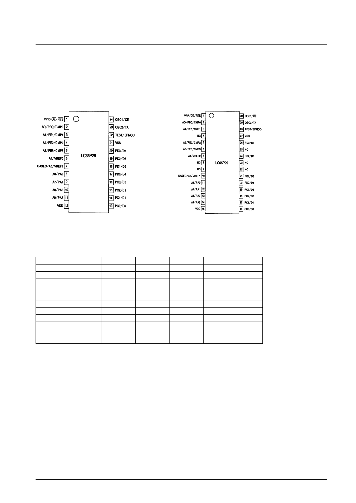
Pin Assignments
DIP24S
Type number. Number of pins ROM capacity RAM capacity Package
LC6527N/F/L, LC6528N/F/L 18 1K, 0.5K 64W, 32W DIP18, MFP18
LC6529N/F/L 24/30 1K 64W DIP24S, SSOP24, MFP30S
LC65E29 24/30 1K 64W DIC24S, MFC30S
LC65P29 24/30 1K 64W DIP24S, MFP30S
LC6543N/F/L, LC6546N/F/L 30 2K, 1K 128W, 64W DIP30S, MFP30S
LC65E43 30 2K 128W, 64W DIC30S, MFC30S
LC65P43 30 2K 128W, 64W DIP30S, MFP30S
LC651104N/F/L, LC651102N/F/L 30 4K, 2K 256W DIP30S, MFP30S
LC651204N/F/L, LC651202N/F/L 30 4K, 2K 256W DIP30S, MFP30S
LC65E1104 30 4K 256W DIC30S, MFC30S
LC65P1104 30 4K 256W DIP30S, MFP30S
MFP30S
Top view Top view
Page 3
Usage Notes
The LC65P29 is designed for program development and evaluation for systems that use the LC6529N/F/L. The following
points require attention when using this product.
• Mounting notes
Due to the nature of the device, one-time programmable microcontrollers cannot be fully tested prior to shipment. This
means that users must perform the screening process described on page 14.
• ROM ordering procedure when using the Sanyo for-fee ROM writing service
The customer must abide by the following when using the Sanyo for-fee ROM writing service:
— When ordering both one-time programmable and mask versions at the same time
The customer must provide an EPROM for the mask version, the mask version order forms, and the one-time
programmable version order forms.
— When order only the one-time programmable version
The customer must provide an EPROM for the one-time programmable version and the one-time programmable
version order forms. The end area in the EPROM (locations 400 to 404H) is the option specification area and the
customer must program the option specification data in that area. The customer must use the cross assembler
specified by Sanyo.
• Differences between the LC65P29 and the LC6529N/F/L
No. 5894-3/14
LC65P29
Parameter LC65P29 LC6529N LC6529F LC6529L
OptionCharacteristicOther items
Ports C and D output option
during reset
High or low can be
specified (option code)
High or low can be specified (mask option)
Port output type during reset
Open-drain output only
(ports A, C, and D)
Open-drain or pull-up register can be specified (mask option)
Oscillator circuit option
CF/RC or EXT can be
specified (option code)
CF/RC or EXT can be
specified (mask option)
CF or EXT can be
specified (mask option)
CF/RC or EXT can be
specified (mask option)
Divider circuit option
1/1, 1/3, or 1/4 can be
specified (option code)
1/1,1/3 or 1/4 can be
specified (mask option)
Only 1/1 is possible
(mask option)
1/1,1/3 or 1/4 can be
specified (mask option)
Comparator input and port E input
option
Comparator or port E can
be specified (option code)
Comparator or port E can be specified (mask option)
Comparator function option
Feedback resistor present
or absent can be specified
(option code)
Feedback resistor present or absent can be specified (mask option)
Minimum cycle time
0.92 µs (VDD≥ 3.0 V) 2.77 µs (VDD≥ 3.0 V) 0.92 µs (VDD≥ 3.0 V) 3.84 µs (VDD≥ 2.2 V)
Operating temperature –30 to +70°C –40 to +85°C
Supply voltage 3.0 to 6.0 V 3.0 to 6.0 V 3.0 to 6.0 V 2.2 to 6.0 V
Current drain 5.0 mA typ. 2.0 mA typ. 2.5 mA typ. 2.0 mA typ.
Reset port input low-level current –50 µA typ. –10 µA typ.
Package DIP24S, MFP30S DIP24S, SSOP24, MFP30S
Page 4
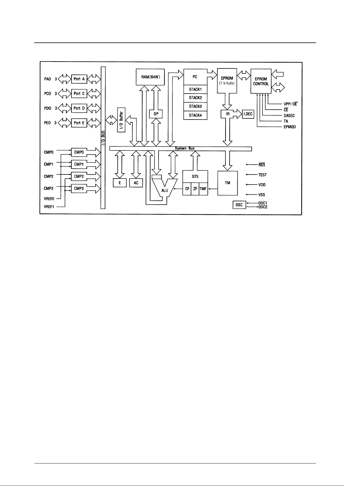
System Block Diagram
No. 5894-4/14
LC65P29
RAM:Data memory
ALU: Arithmetic and logic unit
DP: Data pointer
E: E register
AC: Accumulator
OSC: Oscillator circuit
TM: Timer
STS: Status register
EPROM: Program memory
PC: Program counter
I.R: Instruction register
I.DEC: Instruction decoder
CF: Carry flag
ZF: Zero flag
TMF: Timer overflow flag
to
toto
to
to
A0 to A9
D0 to D7
Page 5

No. 5894-5/14
LC65P29
Pin Descriptions
Pin name
Number
I/O Function Option State during reset
Function in
of pins PROM mode
Power supply. Must be connected to +5 V
during normal operation.
Power supply. Must be connected to 0 V
during normal operation.
—
—
V
DD
V
SS
1
1
—
—
System clock oscillator connections. Leave
OSC2 open and input the external clock to
OSC1 if an external clock is used.
1.Two-pin RC oscillator
(Single-pin external
clock input)
2.Two-pin ceramic
oscillator
3.Divisor option: 1/1, 1/3,
or 1/4
EPROM contorol
signal inputs
CE
TA
OSC1/CE
OSC2/TA
1
I
O
• I/O ports A0 to A3
Input in 4-bit units (IP instruction)
Output in 4-bit units (OP instruction)
Data testing in 1-bit units (BP and BNP
instructions)
Data set and clear operations in 1-bit units
(SPB and RPB instructions)
• PA3 is used for standby mode control.
• Applications must assure that chattering
(key bounce) noise is not input during a
HALT instruction execution cycle.
Open-drain output
• High-level output (The
n-channel output
transistor turned off.)
• Address inputs
A6 to A9
PA0/A6
PA1/A7
PA2/A8
PA3/A9
4 I/O
• I/O ports C0 to C3
The pin functions are identical to those of
pins A0 to A3.
However, there is no standby mode
control function.
• The output during a reset can be specified
to be either high or low as an option.
1. Open-drain output
2. High-level output
during reset
3. Low-level output
during reset
• Selection of items 2 or
3 is in 4-bit units.
• High-level output
• Low-level output
(Depending on an
option selection.)
• Data I/O
D0 to D3
PC0/D0
PC1/D1
PC2/D2
PC3/D3
4 I/O
• I/O ports D0 to D3
The pin functions are identical to those of
pins PC0 to PC3.
The same as for pins
PC0 to PC3
The same as pins PC0 to
PC3
• Data I/O
D4 to D7
PD0/D4
PD1/D5
PD2/D6
PD3/D7
4 I/O
• When comparator input is selected:
CMP0 and CMP1 use V
REF
0 as the
reference voltage,
CMP2 and CMP3 use V
REF
1 as the
reference voltage,
• Comparator inputs CMP0 to CMP3
Data input in 4-bit units (IP instruction)
• Data testing in 1-bit units (BP and BNP
instructions)
1. Comparator input
2. Port E input
3. No feedback resistor
4. Feedback resistor
present
• Selection of items 1 or
2 is in 4-bit units.
• Items 3 and 4 are only
specified when item 1
is selected.
• Address inputs
A0 to A3
PE0/CMP0/A0
PE1/CMP1/A1
PE2/CMP2/A2
PE3/CMP3/A3
4 I
• Comparator reference voltage inputs
V
REF
0 and V
REF
1
V
REF
0 is the reference voltage input for
CMP0 and CMP1.
V
REF
1 is the reference voltage input for
CMP2 and CMP3.
• When PE0/CMP0 to PE3/CMP3 are
selected to function as port E inputs,
these pins are connected to V
SS
.
• Address inputs
A4 and A5
• EPROM control
signal input
DASEC
V
REF
0/A4
V
REF
1/A5/
DASEC
2 I
• System reset input
• Connect an external capacitor to effect the
power-on reset.
• Input a low level for at least 4 clock cycles
to effect a reset restart.
• EPROM control
signal input
V
PP
/ OE
RES/V
PP
/OE
1 I
• IC test pin
This pin must be connected to V
SS
during
normal operation.
• EPROM control
signal input
EPMOD
TEST/EPMOD 1 I
• When input is selected for port E
• Input ports E0 to E3
Input in 4-bit units (IP instruction)
• Data testing in 1-bit units (BP and BNP
instructions)
4 I
Page 6

User Options
• Ports C and D output level during reset option
One of the following two options for the output level during a reset can be selected for each of the ports C and D in
4-bit units.
• Port output circuit type option
The I/O ports A, C, and D are always set up as open-drain outputs.
No. 5894-6/14
LC65P29
Option Conditions and notes
High-level output at reset Ports C and D in 4-bit units
Low-level output at reset Ports C and D in 4-bit units
Option Circuit
Open-drain output (OD)
• Oscillator circuit options
Option Circuit Conditions and notes
The OSC2 pin must be left open.External clock
Two-pin RC oscillator
Two-pin ceramic oscillator
• Divisor option
Option Circuit Conditions and notes
Can be used with any of the 3 oscillator options. (N, F,
and L versions)
Can only be used with the external clock and ceramic
oscillator options. (N and L versions)
Can only be used with the external clock and ceramic
oscillator options. (N and L versions)
No divisor (1/1)
Divide-by-3 circuit (1/3)
Divide-by-4 circuit (1/4)
Page 7

• Comparator input/port E input option
Whether the 4 port pins PE0/CMP0, PE1/CMP1, PE2/CMP2, and PE3/CMP3 function as comparator inputs or as port
E inputs can be selected.
No. 5894-7/14
LC65P29
Option Conditions and notes
Comparator inputs All 4 bits specified together
Port E inputs All 4 bits specified together
• Comparator function option
One of two options relating to the comparator function can be selected.
Usage Procedures
• Option specification procedures
User options can be selected interactively by running the LC6529 option entry software (SU60K). This creates an
option file (file.opt).
Assembling the user program with the macro assembler (M60K) creates an object file. An evaluation file (file.eva) can
be created by linking the object file and the option file with the linker (L60K). Then, a HEX format object file, which
includes both the user program and the mask options, can be created by converting the evaluation file with the file
conversion software (E2H60K). This creates the option codes in the option specification area (locations 400 to 404H).
It is also possible to store data directly to the option specification area. Refer to the option code creation table on page 9
to do this.
Refer to the “LC65/66K Software Manual” for details.
• EPROM programming procedure
A general-purpose EPROM programmer can be used to write the created data to the LC65P29 by using a specialpurpose write conversion board (either the W65EP29D or the W65EP29M).
— The EPROM programmers listed below can be used.
— The “27512 (VPP: 12.5 V) Intel fast write” method must be used for writing. Specify locations 0 to 404 as the
address settings, and make sure that the DASEC jumper is in the off position.
• Using the data security function
The data security function is a function that prevents data written previously to the microcontroller EPROM from being
read out. Use the following procedure to apply the data security to the LC65P29.
1. Set the DASEC jumper on the write conversion board to the on position.
2. Write the data once again.
At this point, the EPROM writer will indicate an error since this function has operated, but actually, no error has
occurred in either the programmer or the IC.
Notes: • The data security function will not be applied if the data value FF is written to all address in step 2.
• The data security function will not be applied if the sequence BLANK → PROGRAM → VERIFY is performed
at step 2.
• Always return the jumper to the off position after performing this procedure.
Option Circuit Conditions and notes
The comparator can be used without hysteresis.
When used with an added external resistor, the
comparator can be used with hysteresis.
No feedback resistor
Feedback resistor present
Manufacturer Models that can be used
ADVANTEST R4945, R4944A, R4943 or equivalent
ANDO —
AVAL —
MINATO Electronics —
Page 8

LC65P29 (DIP24S)
Pin 1
Insert the LC65P29 into the socket correctly
No. 5894-8/14
LC65P29
LC65P29 (MFP30S)
Pin 1
W65EP29D
Pin 1
DASEC setting
• For normal writing • For writing with the security function applied
SW DASEC SW DASEC
W65EP29M
Pin 1
Page 9

• Option data area and definition
Bits specified to be 0 must be set to 0.
00 ... Illegal value
01 ... Illegal value
10 ... Two-pin RC oscillator, 1-pin external drive
(2PORT RC OSC, 1PORT EXT)
11 ... Two-pin ceramic oscillator
(2PORT CF OSC)
Oscillator divider specification
Oscillator type specification
00 1/1 (direct)
01 1/3
10 1/4
11 ... Illegal value
Port C output level at initial reset
0 Low-level output
1 High-level output
Port D output level at initial reset
0 Low-level output
1 High-level output
Comparator function specification
0 No feedback resistor
1 Feedback resistor present
Port input function specification
0 Comparator input
1 Port E input
Port C output type specification
0 Open-drain output
1 Pull-up resistor output
Port A output type specification
Port C output type specification
These bits must be set to 0.
Note: Although all ports are set up to be open-drain outputs regardless of the port option data in the LC65P29, be sure to specify the port option data if you
are using the LC6529N/F/L (mask ROM version).
0 Open-drain output
1 Pull-up resistor output
These bits must be set to 0.
0 Open-drain output
1 Pull-up resistor output
These bits must be set to 0.
Port D output type specification
0 Open-drain output
1 Pull-up resistor output
No. 5894-9/14
LC65P29
Page 10

No. 5894-10/14
LC65P29
Parameter Symbol
Applicable
Conditions
Ratings
Unit
pins/notes min typ max
Maximum supply voltage V
DD
max V
DD
–0.3 +7.0 V
Output voltage V
O
OSC2 Values up to the generated voltage
are allowed. V
VI1 OSC1*
1
–0.3 VDD+ 0.3 V
Input voltage
V
I
2 TEST, RES –0.3 VDD+ 0.3 V
V
I
3
Ports with
–0.3 VDD+ 0.3 V
PE specifications
I/O voltage V
IO
PA, PC, PD –0.3 +15 mA
Peak output current I
OP
PA, PC, PD –2 +20 mA
I
OA
PA, PC, PD The 100 ms average per pin –2 +20 mA
Average output current
Σ I
OA
1 PA The total current for pins PA0 to PA3*
2
–6 +40 mA
Σ I
OA
2 PC, PD
The total current for pins PC0 to PC3 and
–14 +90 mA
PD0 to PD3*
3
Allowable power dissipation
Pdmax1 Ta = –30 to +70°C(DIP24S) 360 mW
Pdmax2 Ta = –30 to +70°C(MFP30S) 150 mW
Operating temperature Topr –30 +70 °C
Storage temperature Tstg –55 +125 °C
Absolute Maximum Ratings at Ta = 25°C, V
SS
= 0 V
Parameter Symbol
Applicable
Conditions
Ratings
Unit
pins/notes V
DD
[V] min typ max
Operating supply voltage V
DDVDD
3.0 6.0 V
Standby supply voltage V
ST
V
DD
RAM and register retention * 1.8 6.0 V
V
IH
1 PA, PC, PD Output n-channel transistor off 0.7 V
DD
13.5 V
V
IH
2 PE
When the port E input option
0.7 V
DD
V
DD
V
High-level input voltage
is selected
V
IH
3 RES 1.8 to6.0 0.8 V
DD
V
DD
V
V
IH
4 OSC1
When the RC oscillator and
0.8 V
DD
V
DD
V
external clock option is selected
VIL1 PA, PC, PD Output n-channel transistor off V
SS
0.3 V
DD
V
V
IL
2 PE
When the port E input option
V
SS
0.3 V
DD
V
is selected
Low-level input voltage
V
IL
3 OSC1
When the RC oscillator and
V
SS
0.25 V
DD
V
external clock option is selected
VIL4 TEST V
SS
0.3 V
DD
V
V
IL
5 RES V
SS
0.25 V
DD
V
Operating frequency (cycle time)
fop(t
CYC
) 200 (20)
4330 (0.92)
kHz (µs)
Frequency fext(text) OSC1 See Figure 1 200 (20)
4330 (0.92)
kHz (µs)
Pulse width
textH, textL
OSC1 See Figure 1 69 ns
Rise and fall times
textR, textF
OSC1 See Figure 1 50 ns
Cext OSC1, OSC2 See Figure 2 4 to 6 220 ±5% pF
Two-pin RC oscillator
Cext OSC1, OSC2 See Figure 2 220 ±5% pF
Rext OSC1, OSC2 See Figure 2 4 to 6 6.8 ±1% kΩ
Rext OSC1, OSC2 See Figure 2 15.0 ±1% kΩ
Ceramic oscillator See Figure 2 See Table 1
Allowable Operating Conditions at Ta = –30 to +70°C, VSS= 0 V, VDD= 3.0 to 6.0 V
Notes: 1. Values up to the generated oscillator amplitude are allowed when driven internally using the guaranteed circuit constant values with the oscillator
circuit shown in figure 2.
2. The average over a 100 ms period.
Note *: Applications must maintain the operating supply voltage (V
DD
) until the IC has entered the standby state when a HALT instruction is executed.
Also, applications must assure that chattering (key bounce) noise is not input to the PA3 pin during a HALT instruction execution cycle.
External clock
conditions
Guaranteed oscillator
circuit constants
Page 11

No. 5894-11/14
LC65P29
Parameter Symbol
Applicable
Conditions
Ratings
Unit
pins/notes V
DD
[V] min typ max
Output n-channel transistor off
I
IH
1 PA, PC, PD
(Includes the n-channel
5.0 µA
transistor off leakage current)
V
IN
= 13.5 V
High-level input current
I
IH
2 PE
When the port E input option
5.0 µA
is selected V
IN
= V
DD
When the RC oscillator and
IIH3 OSC1
external clock option is selected
1.0 µA
V
IN
= V
DD
Output n-channel transistor off
IIL1 PA, PC, PD
(Includes the n-channel
–1.0 µA
transistor off leakage current)
V
IN
= V
SS
Low-level input current
I
IL
2 PE
When the port E input option –1.0 µA
is selected V
IN
= V
SS
IIL3 RES VIN= V
SS
–80 –50 µA
When the RC oscillator and
IIL4 OSC1
external clock option is selected
–1.0 µA
V
IN
= V
SS
VOL1 PA, PC, PD IOL= 10 mA 1.5 V
Low-level output voltage VOL2 PA, PC, PD
I
OL
= 1.8 mA
0.4 V(When all port I/O levels are
Under 1 mA)
Hysteresis voltage
V
HIS
1 RES 0.1 V
DD
V
V
IHS
2 OSC1*
1
When the RC oscillator and
0.1 V
DD
V
external clock option is selected
RC oscillator
ID
DOP
1 V
DD
Figure 2. 850 kHz (TYP) 5 8 mA
ID
DOP
2 V
DD
Figure 2. 400 kHz (TYP) 4.5 7 mA
ID
DOP
3 V
DD
Figure 3. 4 MHz, 1/1, 1/3, and
5 8 mA
1/4 divisor ratios
ID
DOP
4 V
DD
Figure 3. 2 MHz, 1/1, 1/3, and
4.5 7 mA
Ceramic oscillator*
2
1/4 divisor ratios
ID
DOP
5 V
DD
Figure 3. 800 kHz, 1/1 divisor
5 8 mA
ratio
ID
DOP
6 V
DD
Figure 3. 400 kHz, 1/1 divisor
4.5 7 mA
ratio
External clock*
2
ID
DOP
7 V
DD
200 to 4330 kHz, 1/1, 1/3, and 5 8 mA
1/4 divisor ratios
IDDst1 V
DD
Output n-channel transistor off
6 0.05 10 µA
Standby mode
Port = V
DD
IDDst2 V
DD
Output n-channel transistor off
3 0.025 5 µA
Port = V
DD
OSC1, OSC2
Figure 2. Cext = 220 pF ±5%
275 400 711 kHz
Oscillator frequency fMOSC
Rext = 15.0 kΩ ±1%
OSC1, OSC2
Figure 2. Cext = 220 pF ±5%
4 to 6 579 850 1179 kHz
Rext = 6.8 kΩ ±1%
OSC1, OSC2 Figure 3. fo = 4 MHz 3840 4000 4160 kHz
Oscillator frequency fFOSC*
3
OSC1, OSC2 Figure 3. fo = 2 MHz 1920 2000 2080 kHz
OSC1, OSC2 Figure 3. fo = 800 kHz 768 800 832 kHz
OSC1, OSC2 Figure 3. fo = 400 kHz 384 400 416 kHz
Figure 4. fo = 4 MHz 10 ms
Oscillator stabilization time tCFS
Figure 4. fo = 2 MHz
fo = 800 kHz 10 ms
fo = 400 kHz
Pull-up resistor reset port Ru V
IN
= V
SS
5 70 100 150 kΩ
External reset characteristics:
tRST
See Figure 6.
ms
reset time
f = 1 MHz
Pin capacitance Cp V
IN
= VSSfor all input pins 10 pF
other than the measured pin
Electrical Characteristics at Ta = –30 to +70°C, VSS= 0 V, VDD= 3.0 to 6.0 V
Current drainOscillator characteristics
RC oscillator
Ceramic oscillator
Notes: 1. The OSC1 pin has Schmitt characteristics when the RC oscillator and external clock input oscillator option is selected.
2. The current drain during normal operation with the output n-channel transistors off and the port at V
DD
.
3. fCFOSC indicates frequencies at which oscillator operation is possible.
Page 12

No. 5894-12/14
LC65P29
Parameter Symbol
Applicable
Conditions
Ratings
Unit
pins/notes V
DD
[V] min typ max
Reference input voltage range VRF
INVREF
0, 1 VSS+ 0.3 VDD– 1.7 V
Common-mode input voltage range VCM
IN
CMP0 to 3 V
SS
VDD– 1.7 V
Offset voltage V
OFF
VCMIN = VSSto VDD– 1.7 V ±50 ±300 mV
Response speed
TRS1 See Figure 5. 4 to 6 1.0 5.0 µs
TRS2 See Figure 5. 1.0 200 µs
I
IH
1 V
REF
0, 1 1.0 µA
High-level input current
I
IH
2 CMP0 to 3
When the feedback resistor
5.0 µA
option is not selected
I
IL
1 V
REF
0, 1 –1.0 µA
Low-level input current
I
IL
2 CMP0 to 3
When the feedback resistor
–1.0 µA
option is not selected
Feedback resistance RCMFB CMP0 to 3
When the feedback resistor
460 kΩ
option is selected
Comparator characteristics (When the comparator input option is selected)
at Ta = –30 to +70°C, VSS= 0 V, VDD= 3.0 to 6.0 V
Table 1 Guaranteed Ceramic Oscillator Circuit Constants
Figure 1 External Clock Input Waveform
Standard type Chip type
Oscillator type
Manufacturer
Oscillator
C1 C2 Rd Manufacturer
Oscillator
C1 C2
element element
4 MHz
Murata Mfg. Co., Ltd.
CSA4.00MG 33 pF ±10% 33 pF ±10% —
Murata Mfg. Co., Ltd.
CSAC4.00MGC 33 pF ±10% 33 pF ±10%
Kyocera Corporation
KBR-4.0MSA 33 pF ±10% 33 pF ±10% — — — — —
2 MHz
Murata Mfg. Co., Ltd.
CSA2.00MG 33 pF ±10% 33 pF ±10% —
Murata Mfg. Co., Ltd.
CSAC2.00MGC 33 pF ±10% 33 pF ±10%
Kyocera Corporation
KBR-2.0MS 47 pF ±10% 47 pF ±10% — — — — —
800 kHz
Murata Mfg. Co., Ltd.
CSB800J 100 pF ±10% 100 pF ±10% 3.3 KΩ — — — —
Kyocera Corporation
KBR-800F/Y 150 pF ±10% 150 pF ±10% — — — — —
400 kHz
Murata Mfg. Co., Ltd.
CSB400P 220 pF ±10% 220 pF ±10% 3.3 KΩ — — — —
Kyocera Corporation KBR-400BK/Y
330 pF ±10% 330 pF ±10% — — — — —
4 MHz
Murata Mfg. Co., Ltd.
CST4.00MGW
— — — — — — —
Kyocera Corporation
KBR-4.0MKS — — —
Kyocera Corporation
KBR-4.0MWS — —
2 MHz
Murata Mfg. Co., Ltd.
CST2.00MG
— — — — — — —
— — — — —
Kyocera Corporation
KBR-2.0MWS — —
External capacitor type
Internal capacitor type
Page 13

No. 5894-13/14
LC65P29
Figure 2 Two-Pin RC Oscillator Circuit Figure 3 Ceramic Oscillator Circuit
Figure 4 Oscillator Stabilization Time
Figure 5 Comparator Response Speed TRS Timing
Note: The reset period due to a CRES with a value of 0.68 µF will be 10 to 100 ms
when the power supply rise time is zero.
If the power supply rise time is relatively long, increase the value of CRES
so that the reset time is at least 10 ms, which is the oscillator stabilization
time.
Figure 6 Reset Circuit
Page 14

PS No. 5894-14/14
LC65P29
Notes on Mounting Preconditions for One-Time Programmable Microcontrollers
This product is provided in both DIP and MFP packages. Since the mounting preconditions are different for these two
package types, implement the flowchart appropriate for the product used.
See the following item for details on the screening conditions.
Notes on One-Time Programmable Microcontroller Screening
Due to the structure of their circuits, it is not possible for Sanyo to fully test one-time programmable microcontroller
products before the PROM has been written. To increase the reliability after the PROM has been written, we strongly
recommend screening these products after writing according to the following flowchart.
This catalog provides information as of June, 1998. Specifications and information herein are subject to change
without notice.
■ No products described or contained herein are intended for use in surgical implants, life-support systems, aerospace
equipment, nuclear power control systems, vehicles, disaster/crime-prevention equipment and the like, the failure of
which may directly or indirectly cause injury, death or property loss.
■ Anyone purchasing any products described or contained herein for an above-mentioned use shall:
➀ Accept full responsibility and indemnify and defend SANYO ELECTRIC CO., LTD., its affiliates, subsidiaries and
distributors and all their officers and employees, jointly and severally, against any and all claims and litigation and all
damages, cost and expenses associated with such use:
➁ Not impose any responsibility for any fault or negligence which may be cited in any such claim or litigation on
SANYO ELECTRIC CO., LTD., its affiliates, subsidiaries and distributors or any of their officers and employees
jointly or severally.
■ Information (including circuit diagrams and circuit parameters) herein is for example only; it is not guaranteed for
volume production. SANYO believes information herein is accurate and reliable, but no guarantees are made or implied
regarding its use or any infringements of intellectual property rights or other rights of third parties.
Due to the structure of the one-time programmable microcontroller PROM circuit in the state before writing, it is not
possible to write test all the bits in the device. This means that it is impossible to guarantee a yield of 100%.
Recommended Screening Flowchart
High-temperature bake
with no power applied
+1
150 ±5°C, 24 Hr
–0
Program readout
verification
V
DD
= 5 V ±0.5 V
DIP product
Program write and verify
Screening
Mounting
MFP product
Program write and verify
Screening
Mounting
 Loading...