

Page 1
Ordering number : ENN*6829
LC65F1306A
4-Bit Single-Chip CMOS Microcont roller for
Small-Scale Control Applications
Preliminary
Overview
The LC65F1306A belongs to our 4-bit single-chip microcontroller LC6500 series fabricated using CMOS process
technology. They are ideally suited for use in small-scale control applications. Their basic architecture and instruction set
are the same. These microcontrollers include an 8-input 8-bit A/D converter and are appropriate for use in a wide range of
applications. That range includes applications with a small number of control circuits that were previously implemented in
standard logic, and applications with a larger scale such as home appliances, automotive equipment, communications
equipment, office equipment, and audio equipment such as decks and players. This microcontroller, with some exceptions,
has identical functions to the LC651306A, 1304A, 1302A and 1301A mask ROM version microcontrollers. It can also be
used as an OTP version microcontroller. Further, through a rewrite operation on the FLASH memory, the LC65F1306A can
be used in applications where previously microcontrollers of this type could not have been implemented.
Features
1) CMOS technology for a low-power consumption operation (A standby function that can be invoked under program
control is also provided.)
2) Flash ROM/RAM
LC65F1306A Flash ROM : 6K × 8 bits, RAM : 256 × 4 bits
3) Instruction set : 81 instructions common to all microcontrollers of the LC6500 series
4) Wide operating voltage range : 3.0 V to 5.5 V
5) Instruction cycle time : 0.92 µs
6) On-chip serial I/O port
CMOS IC
Ver.1.01
62600
N3000 RM (IM) TY No.6829-1/22
Page 2

LC65F1306A
7) Flexible I/O port
• Number of ports : 5 ports / 18 pins (max.)
• All ports : Input / output common
Input / output capacity voltage 15V max. (open-drain specification C and D only)
Output current 20 mA max. sink curren t (Ca n drive an L ED directly)
• Support option for system specification
Output level in the reset mode : high/low level for port C and D specified in 4-bit unit
8) Interrupt function
Interrupt by timer overflow (can be tested under program control)
Interrupt by the state of the
pin or completion of transmission/reception at serial I/O port (can be tested under
INT
program control)
9) Stack level : 8 levels (common use with interrupt)
10) Timer : 4-bit variable prescaler + 8-bit programmable counter
11) Clock oscillation options for user’s intended system
• Oscillator circuit options : two-pin RC oscillator
two-pin ceramic osci llator
• Divider circuit options : No divider
built-in divide by 3
built-in divide by 4
12) Continuous square wave output (64 times of the cycle time)
13) AD converter (successive approximation)
• Precise conversion (expressed in 8 bits), 8 input channels
14) Watchdog timer
• RC circuit time constant
• Watchdog timer reset function can be assigned to an external pin by the option.
15) Low voltage detection circuit
• Can be implemented by the option.
16) Factory shipment
• DIP24S, MFP24S
17) Flash Memory
• Rewrite block size : 128 bytes / page
• Erase / write voltage : 3.0 to 5.5V
• Rewritable limit : 10000 times (target number, to be decided after evaluation)
• Operating temperature : 0 to +85°C (when writing to the flash m emory)
-20 to +85°C (when reading from the flash memory)
No.6829-2/22
Page 3

LC65F1306A
Function Table
Parameter LC651306A/04A/02A/01A LC65F1306A
Memory
On-chip
functions
I/O ports
Characteristics
Oscillator
Other items
Note: The above oscillator and oscillator circuit constants are tentative. They will be announced as the recommended circuits
for these microcontrollers are determined. Please confirm the progress of these developments periodically.
ROM
RAM
Instruction set 81 81 Instructions
Table reference Supported Supported
Interrupt 1 external, 1 internal 1 external, 1 internal
Timer 4-bit variable prescaler + 8-bit
Stack level 8 8
Standby function Standby mode by the HALT
Port number 18 I/O port pins 22 I/O port pins
Serial port Input and output in 4 or 8 bit
I/O voltage
capacity
Output current 10 mA typ. 20 mA max. 10 mA typ. 20 mA max.
I/O circuit type Open drain (N-channel) or
Output level at
reset
Square wave output Supported Supported
Minimum cycle
time
Operating
temperature
Supply voltage 2.5 to 6 V 3.0 to 5.5 V
Supply current 1.5 mA typ. 3 mA typ.
Oscillator RC (800 kHz typ.)
Divider circuit
option
Package DIP24S MFP24S SSOP24 DIP24S MFP24S
Watchdog timer Supported Supported
OTP Only DIP24S MFP24S -
6144 × 8 bits (1306A)
4096 × 8 bits (1304A)
2048 × 8 bits (1302A)
1024 × 8 bits (1301A)
256 × 4 bits
(1306A/04A/02A/01A)
4-bit variable prescaler + 8-bit
timers
instruction supported
units
15 V max. 15 V max.
pull-up resistor output option
can be specified in 1- bit unit.
High or low level output can be selected in port unit (ports C and D
only)
0.92 µs (VDD ≥ 2.5 V) 0.92 µs (VDD ≥ 3.0 V)
-40°C to +85°C 0°C to +85°C (when writing)
-20°C to +85°C (when reading)
Ceramic (400k, 800k,1MHz,
4MHz)
1/1, 1/3, 1/4 1/1, 1/3, 1/4
6144 × 8 bits
256 × 4 bits
timers
Standby mode by the HALT
instruction supported
Input and output in 4 or 8 bit
units
Open drain (N-channel)
RC (800 kHz typ.)
Ceramic (400k, 800k,1MHz,
4MHz)
No.6829-3/22
Page 4
LC65F1306A
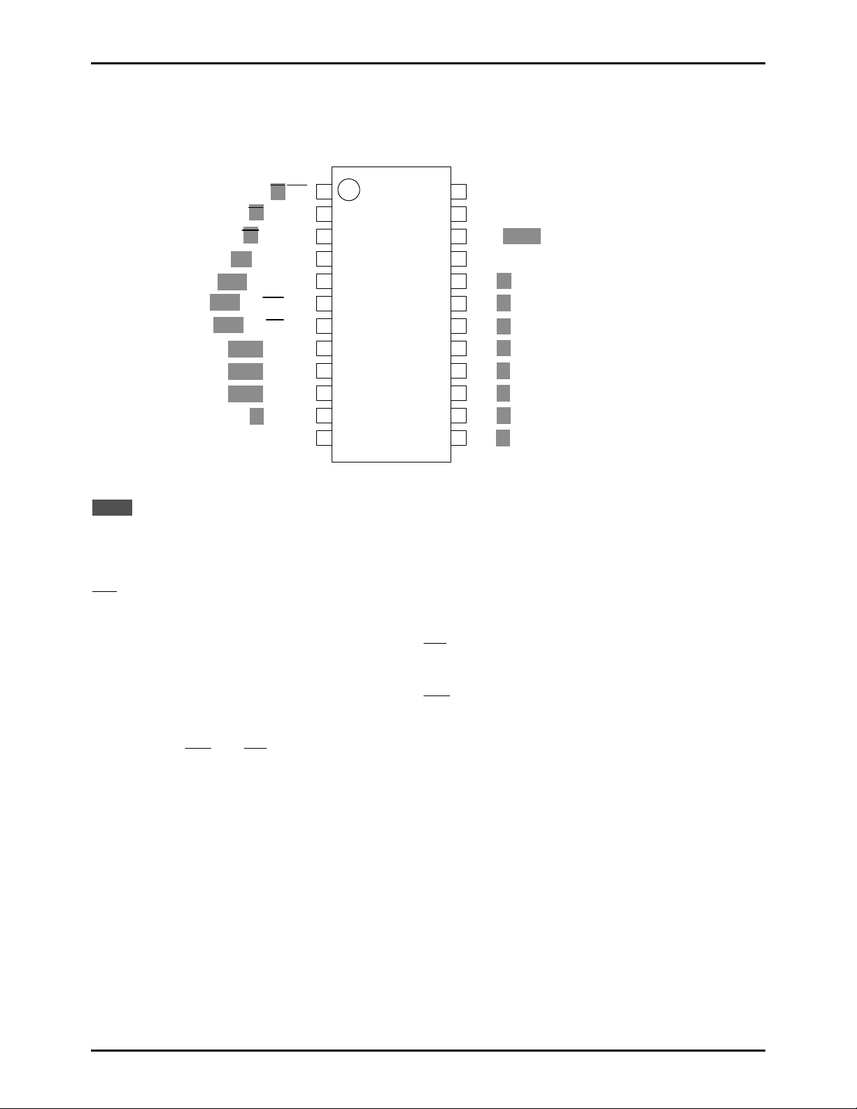
Pin Assignment
DIP24S, MFP24S
/
RES
A0/A7/PF1/SO/AD5
A1/A8/PF2/
A2/A9/PF3/
A3/A10/PA0/AD0
A4/A11/PA1/AD1
A5/A12/PA2/AD2
CE
/PE0/SQR
OE
/PE1/WDR
WE
ALE/PF0/SI/AD4
SCK
INT
A6/PA3/AD3
/AD6
/AD7
VDD
1
2
3
4
5
6
7
8
9
10
11
12
OSC1
24
OSC2
23
TEST/EPMOD
22
VSS
21
PD3/D7
20
PD2/D6
19
PD1/D5
18
PD0/D4
17
PC3/D3
16
PC2/D2
15
PC1/D1
14
PC0/D0
13
: Pin function names used when writing data to on-chip Flash ROM with the PROM writer
Pin Functions
OSC1, OSC2 : Ceramic Oscillator fo r OSC, RC TEST : Test
: Reset AD0-AD7 : AD converter analog input
RES
PA0-3 : Common I/O port A0-3 SQR : Square wave output
PC0-3 : Common I/O port C0-3 WDR : Watch Dog Reset pin
PD0-3 : Common I/O port D0-3
PE0-1 : Common I/O port E0-1 SI : Serial Input pin
PF0-3 : Common I/O port F0-3 SO : Serial Output pin
Notes: • SQR and WDR are common with PE0 and PE1 respectively.
• SI, SO,
SCK
, and
are common with PF0 to PF3 respectively.
INT
: Interrupt Request pin
INT
: Serial Clock input/output pin
SCK
No.6829-4/22
Page 5
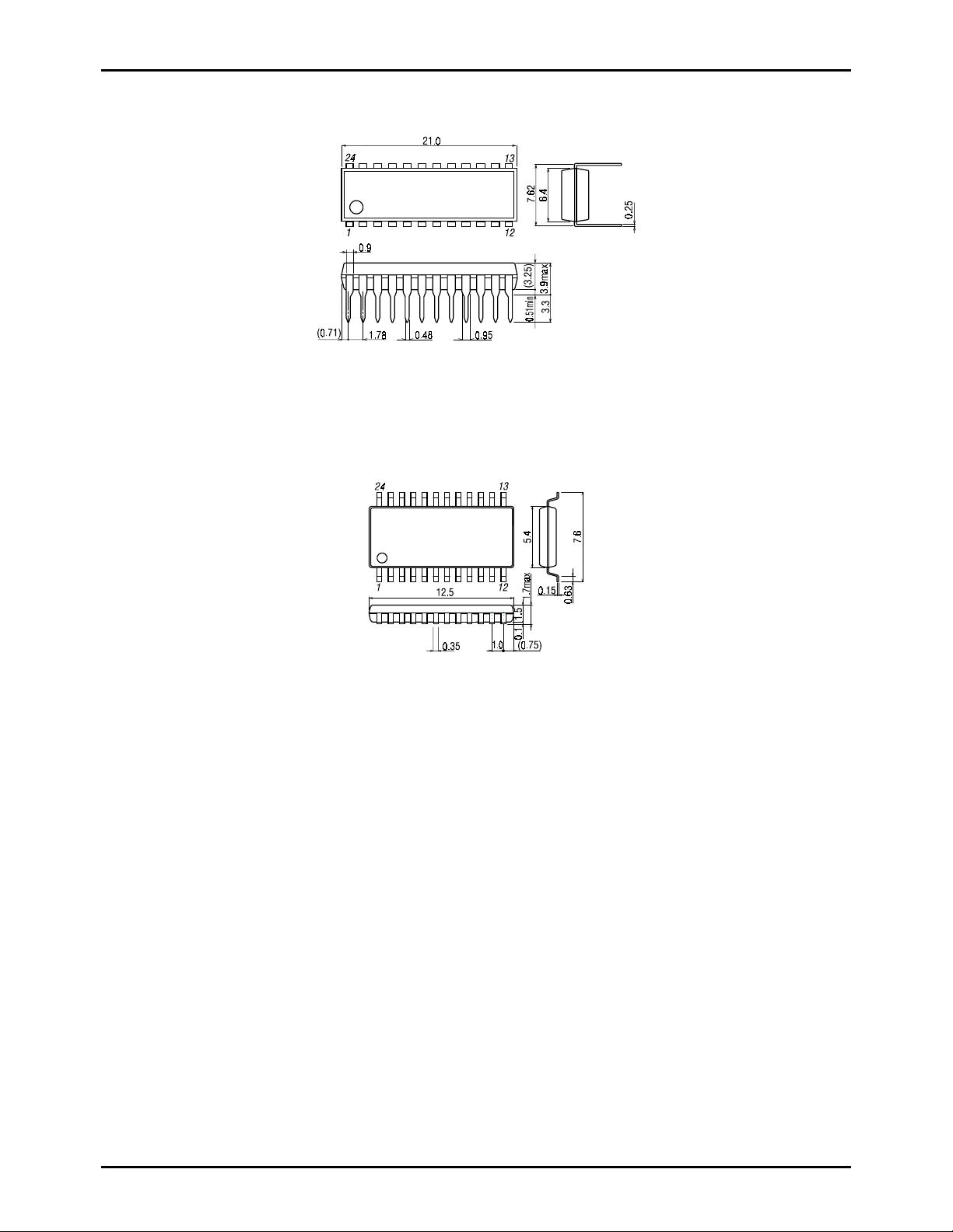
Package Dimension
(unit : mm)
3067A
Package Dimension
(unit : mm)
3112A
LC65F1306A
SANYO : DIP24S(300mil)
SANYO : MFP24S(30 0 mil)
No.6829-5/22
Page 6
LC65F1306A
g
g
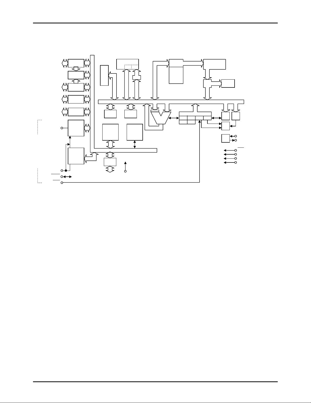
System Bl ock Diagram
LC65F1306A
PF1/SO
Shared with port F
PF0/SI
PF2/SCK
PA0-3
AD0-3
PF0-3
AD4-7
PC0-3
PD0-3
4/8 bit
4 bit
Port A
8-BIT
ADC
Port F
Port C
Port D
Serial
shift
register
lower di
Serial
shift
register
hi
4/8 bit
it
her digit
RAM
I/O Buffer
E AC
Serial
mode
register
Port E
PE0-1
WDR
F WR
Serial
mode
register
I/O Bus
DP
System Bus
ALU
PC
STACK 1
to
STACK 8
CF
CSF ZSF
STS
ZF
FLASH
ROM
IR
EXTF TMF
PF3/INT
RAM : Data Memory FLASH ROM : Program Memory
F : Flag PC : Program Counter
WR : Working Register INT : Interrupt control
AC : Accumulator IR : Instruction Register
ALU : Arithmetic an d L og ic Unit I.DEC : Instruction Decoder
DP : Data Pointer CF, CSF : Carry Flag, Carry Save Flag
E : E register ZF, ZSF : Zero Flag, Ze r o Save Flag
CTL : Control register EXTF : External Interrupt Request Flag
OSC : Oscillation Circuit TMF : Internal Interrupt Request Flag
TM : Timer
STS : Status register
I.DEC
TM CTL
INT
OSC
OSC1
OSC2
RES
TEST
VDD
VSS
No.6829-6/22
Page 7
LC65F1306A
k
P
P
P
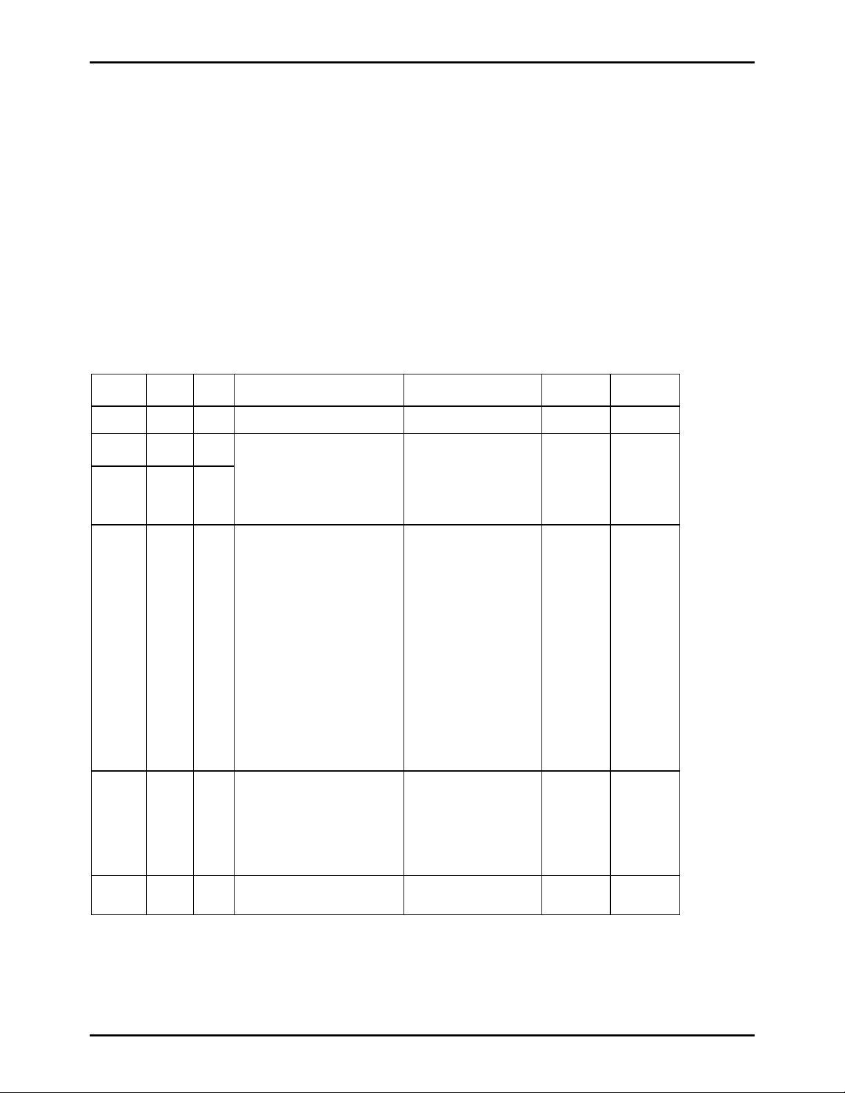
Development Support
The following are currently in the development stage and will soon be available to the user for the development of the
LC65F1306A.
1. User’s manual
Refer to the “LC65F1306A/LC651300 series user’s manual.”
2. Development tool manual
Refer to the “EVA86000 Development Tool Manual for 4-bit microcontrollers.”
3. Software manual
“LC65/66 Series Software Manual”
4. Development tool
a. For program development (EVA86000 system)
b. For program evaluation
Microcontroller with Flash ROM (LC65F1306)
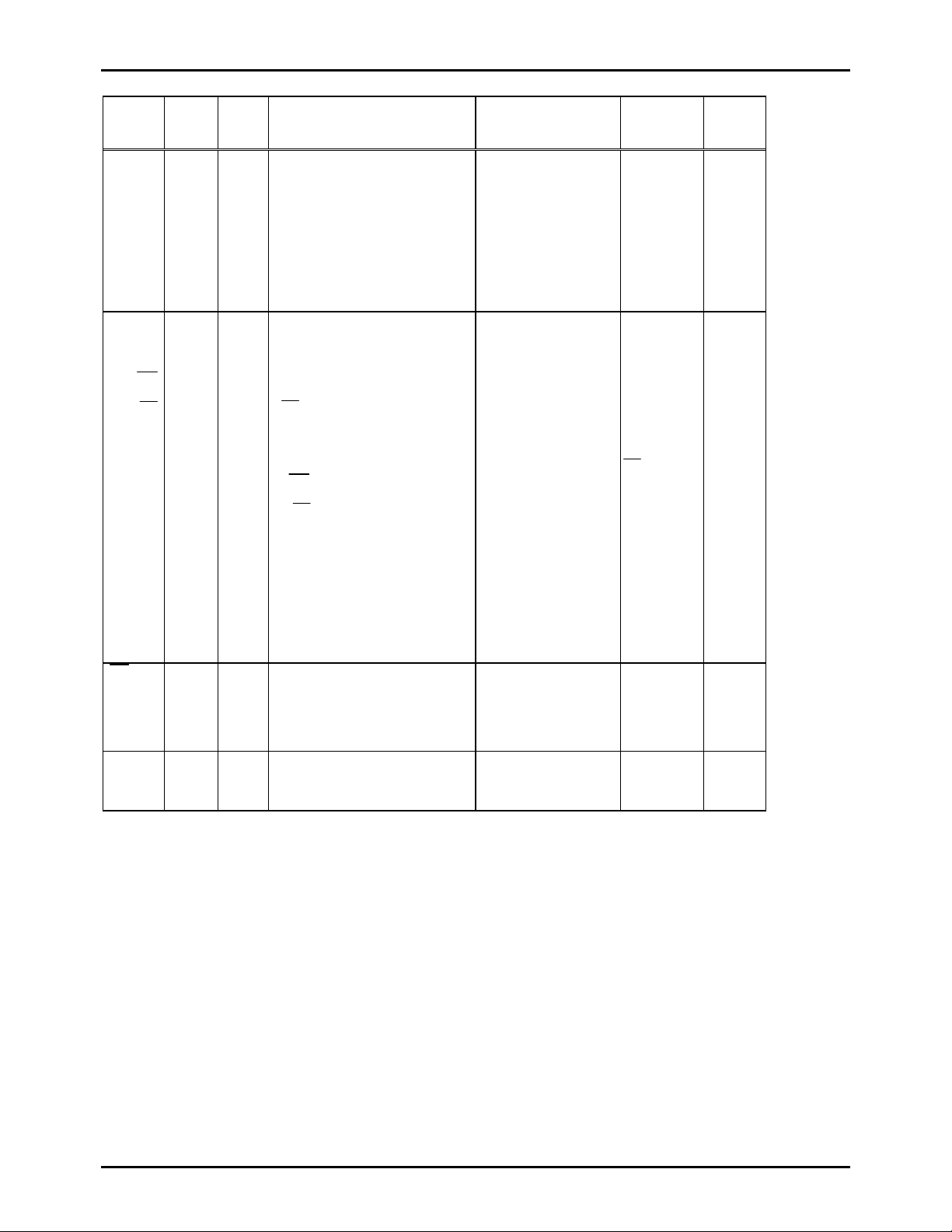
Pin Functions
Symbol
VDD 1 - Power supply - - VSS 1 -
OSC1 1 Input
OSC2 1 Output
PA0-PA3/
AD0-AD3
PC0-PC3 4 I/O •I/O port C0 to C3
PD0-PD3 4 I/O •I/O port D0 to D3
Number
of pins
I/O Function Option At reset
Pins for connecting system cloc
•
oscillation RC or ceramic resonator.
Leave OSC2 open when OSC1 is
•
used for an external clock input
4 I/O • I/O port A0 to A3
Input in 4-bit unit (IP instruction)
Output in 4-bit unit
(OP instruction)
Testing in 1-bit unit
(BP, BNP instructions)
Set and reset in 1-bit unit
(SPB, RPB instructions)
PA3 is used for standby mode
•
control.
Chattering should not be occurred
•
on the PA3 during HALT
instruction execution.
All four pins have shared
•
function.
PA0/AD0:AD converter input AD0
PA1/AD1:AD converter input AD1
PA2/AD2:AD converter input AD2
PA3/AD3: converter input AD3
The port functions are identical to
those of PA0 to PA3 (See note).
The output during a reset can be
•
selected to be either high or low as
an option.
Note: This port has no standby
mode control function.
The port functions and options are
identical to those of PC0 to PC3.
(1) Two-pin RC oscillator,
external clock
(2) Two-pin ceramic oscillator
(3) Divider option
1. No divider
2. Divide by 3
3. Divide by 4
Open-drain output only High-level
Open-drain output only
(1) High level output during
reset.
(2) Low level output during
reset.
(1) and (2) are specified
•
4 bits at a time
Same as PC0 to PC3. Same as PC0 to
- -
output (The
output
N-channel
transistor s in
the off state.)
High-level
•
output.
Low-level
•
output.
(Depending
on options
selected)
C3.
Handling
when unused
Select the
open-drain
output
option and
connect to
VSS.
Same as PA0 to
A3.
Same as PA0 to
A3.
No.6829-7/22
Page 8
LC65F1306A
t
t
Handling
when
unused
Identical to
those for
PA0 to
PA3.
Identical to
those for
PA0 to
PA3.
must be
connected
to VSS.
/WDR
SCK
INT
Number
of pins
I/O Function Option At reset
2 I/O • I/O port E0 to E1
4 I/O • I/O port F0 to F3
1 Input • System reset input
Input in 4-bit unit (IP instruction)
Output in 4-bit unit (OP instruction)
Set and reset in 1-bit unit
(SPB and PRB instructions)
Testing in 1-bit unit
(BP and BNP instructions)
PE0 also has a continuous pulse (64
•
Tcyc) output function.
PE1 becomes the watchdog reset pin
•
WDR when selected as an option.
The port functions and options are
identical to those of PE0 to PE1 (See
note).
PF0 to PF3 have shared functions
•
with the serial interface pins and the
input.
INT
The function can be selected under
program control.
SI... Serial input pin
SO...Serial output pin
...Input and output of the serial
SCK
clock signa l.
...Interrupt request signal
INT
The serial I/O function can be
switched between 4-bit and 8-bit
transfers under program control.
Note: There is no continuous pulse
output function.
All four pins have shared function.
•
PF0/AD4: AD converter input AD4
PF1/AD5: AD converter input AD5
PF2/AD6: AD converter input AD6
PF3/AD7: AD converter input AD7
Provide an external capacitor for the
•
power-on reset.
Apply low level to this pin for 4 or
•
more clock cycles to reset and restart
the program.
This pin must be connected to VSS
during normal operation.
Open -drain output only
(1) Normal port PE1
(2) Watchdog reset WDR
Either options (1) or
•
(2) can be selected.
Identical to those for PA0 to
PA3.
- - -
- - This pin
High level
output (The
output
N-channel
transistors in
the off state)
Identical to
hose for PA0
o PA3.
The serial port
functions are
disabled.
The interrupt
source is set to
.
INT
Symbol
PE0-PE1
PF0/SI/A
D4
PF1/SO/
AD5
PF2/
/AD6
PF3/
/AD7
RES
TEST 1 Input • Test pin for LSI.
No.6829-8/22
Page 9
LC65F1306A
User Option
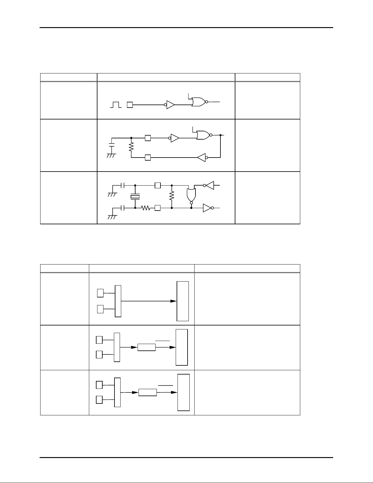
User option is selected according to the information written to the user option area on the on-chip Flash ROM.
Oscillator Circuit Options
Option Circuit Conditions and notes
External clock
Two-pin RC oscillator
Ceramic oscillator
Cext
Ceramic
Resonator
OSC1
C1
C2
OSC1
OSC
Rext
OSC1
OSC2
R
The OSC2 pin should be
left open.
Divider Circuit Options
Option Circuit Conditions and notes
No divider
(1/1)
Built-in
divide-by-three
circuit
Built-in
divide-by-four
circuit
fOSC
Oscillator circuit
• The oscillator frequency or external clock
frequency should not exceed 4330 kHz.
Timing
Generator
fOSC
Divide by 3
fOSC
3
Oscillator circuit
This option can only be used with the
•
external clock and the ceramic oscillator
options.
• The oscillator frequency or external clock
Timing
Generator
frequency should not exceed 4330 kHz.
fOSC
Divide by 4
fOSC
4
Oscillator circuit
• This option can only be used with the
external clock and the ceramic oscillator
options.
• The oscillator frequency or external clock
Timing
Generator
frequency should not exceed 4330 kHz.
Note: The following table summarizes the oscillator and divider circuit options. When selecting the divider option, the
relationship between frequency and cy cle time must be taken into account.
No.6829-9/22
Page 10
LC65F1306A
LC65F1306A Oscillator Options
Circuit type Fr eq uency
Ceramic resonator
External clock (used
with the 2-pin RC
oscillator circuit)
External clock used with
the ceramic oscillator
option
400 kHz
800 kHz
1 MHz
4 MHz
384 k to 4330 kHz
1152 k to 4330 kHz
1536 k to 4330 kHz
recommended circuit constants. When using
other constants by necessity, use the frequency
and VDD range identical to t he external clock
written above.
External clock drive is not possible. To use external clock drive, select the 2-pin RC oscillator option.
Divider option
(Cycle time)
1/1 (10µs)
1/1 (5µs)
1/1 (4µs)
1/1 (1µs)
1/3 (3µs)
1/4 (4µs)
1/1 (10.4 to 0.92µs)
1/3 (10.4 to 2.77µs)
1/4 (10.4 to 3.70µs)
VDD
range
3 to 5.5V Can not be used with the divide-by-three
3 to 5.5V
3 to 5.5V
3 to 5.5V
3 to 5.5V
3 to 5.5V
3 to 5.5V
3 to 5.5V
3 to 5.5V
3 to 5.5V Two-pin RC Use the no divider circuit option and the
and divide-by-four options.
Notes
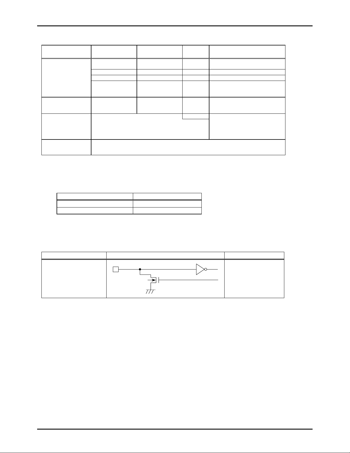
Port C and D Output level Option During Reset
The Output level of the C and D ports at reset can be selected from the following two options in 4-bit unit.
Option Conditions and notes
High level output at reset P orts C and D in 4-bit unit
Low level output at reset Ports C and D in 4-bit unit
Port Output Type
The I/O port type is open-drain output.
Option Circuit Ports
Open-drain output
Ports A, C, D, E and F
Watchdog Reset Option
This option allows the user to select how the PE1/WDR pin is to be used. It can be used as the normal port PE1, or used as the
watchdog reset pin WDR.
No.6829-10/22
Page 11
LC65F1306A
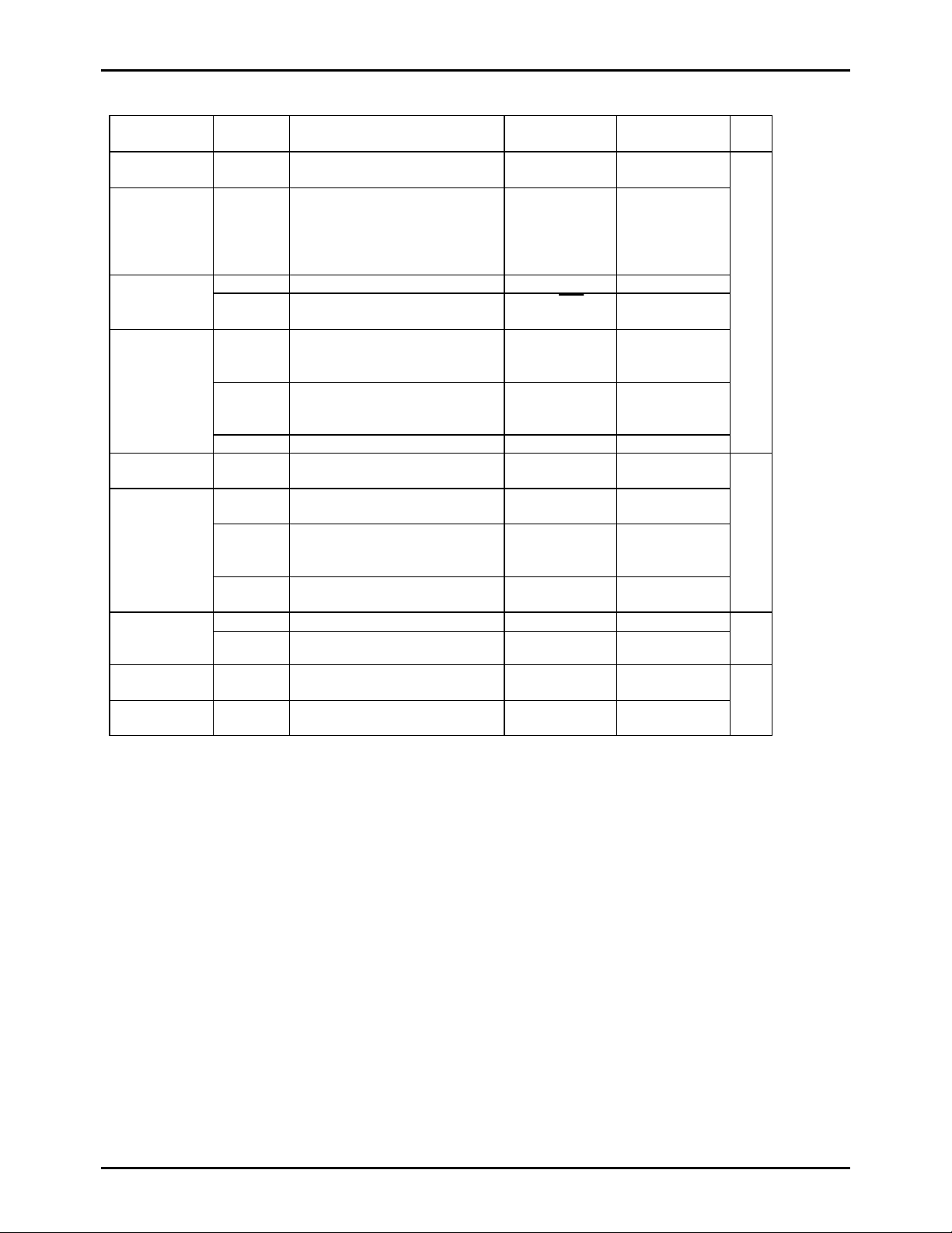
1. Absolute Maximum Ratings at Ta=25°C, VSS=0V
Parameter Symbol Conditions
Maximum
VDD max VDD -0.3 to +6.5
Applicable pins
and notes
Ratings unit
supply voltage
Output voltage VO OSC2 Output voltage
generated can be
over the
maximum limit
of the VDD.
VI (1) OS C1 (Note 1) -0.3 to VDD+0.3 Input voltage
I/O voltage
VI (2) TEST,
AV
+
VIO (1) PC0 to 3, PD0 to 3 Open-drain
RES
, AV-
-0.3 to VDD+0. 3
-0.3 to +15
specification
ports
VIO (2) PC0 to 3, PD0 to 3 Pull-up resistor
-0.3 to VDD+0. 3
specification
ports
VIO (3) PA0 to 3, PE0, 1, PF0 to 3 -0.3 to VDD+0.3
Peak output
IOP I/O Port -2 to +20
current
Average
output current
IOA Average current applied to a pin
for 100 ms
IOA(1)
∑
The total current of PC0 to 3,
PD0 to 3 and PE0 to 1. (N ote 2)
I/O Port -2 to +20
PC0 to 3
-15 to +100
PD0 to 3
PE0 to 1
power
IOA(2)
∑
Pd max (1)
Pd max (2)
The total current of PF0 to 3 and
PA0 to 3. (Note 2)
Ta=-20 to +85°C (DIP package)
Ta=-20 to +85°C (MFP package)
PF0 to 3
-15 to +100
PA0 to 3
310 Maximum
220
consumption
Operating
Topr -20 to +85
temperature
Storage
Tstg -55 to +125
temperature
V
mA
mW
C
°
No.6829-11/22
Page 12
LC65F1306A
k
k
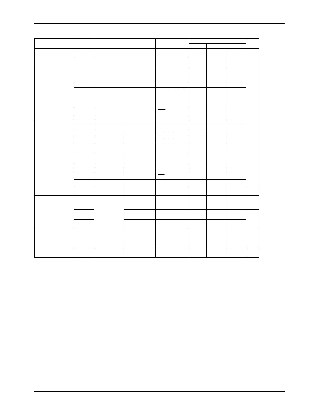
2. Recommended Operating Range at Ta=-20 to +85°C, VSS=0V, VDD=3.0 to 5.5V (Unless otherwise specified)
Parameter Symbol Conditions
Operating supply
voltage
Standby supply
voltage
High level input
voltage
VIH(2) Output Nch Tr. off Port A, E, F 0.7VDD VDD
VIH(3) Output Nch Tr. off
VIH(4) VDD= 1.8 to 5.5 V
VIH(5) External clock sp ecifications OSC1 0.8VDD VDD
Low level
input voltage
Operating frequency
(cycle time)
External clock
conditions
Frequency
Pulse width textH,
Rising/falling time textR,
Recommended
oscillation constants
Two-pin RC
oscillator
Ceramic oscillator
(Note 4)
VDD VDD 3.0 5.5 V
VST RAM and register values retained.
VIH(1) Output Nch Tr. off Port C, D with
VIL(1) Output Nch Tr. offVDD=4 to 5.5V Port VSS 0.3VDD
VIL(2) Output Nch Tr. off3 to 5.5V Port VSS 0.25VDD
VIL(3) Output Nch Tr. offVDD=4 to 5.5 V
VIL(4) Output Nch Tr. off3 to 5.5V
VIL(5) External cloc
VIL(6) External cloc
VIL(7) VDD=4 to 5. 5V TEST VSS 0.3VDD
VIL(8) 3 to 5.5V TEST VSS 0.25VDD
VIL(9) VDD=4 to 5. 5V
VIL(10) 3 to 5.5V
fop
(Tcyc)
text
textL
textF
Cext
Rext
Fig. 3 See Table
(Note 3)
VDD=4 to 5. 5V OSC1 VSS 0.25VDD
specification
3 to 5.5V OSC1 VSS 0.2VDD
specification
VDD=3 to 5.5V 384
Fig. 1
VDD=3 to 5. 5V OSC1
VDD=3 to 5.5V OSC1 69 ns
VDD=3 to 5.5V OSC1 50
Fig. 2 VDD=3 to 5.5V OSC1, OSC2
Applicable pins
and notes
VDD 1.8 5.5
open-drain
specifications.
,
The
and SI pin with
open-drain
specifications.
RES
INT, SCK
INT, SCK
RES
RES
SCK
INT
, SI
, SI
min. typ. max.
0.7VDD 13.5
0.8VDD VDD
,
0.8VDD VDD
VSS 0.25VDD
VSS 0.2VDD
VSS 0.25VDD
VSS 0.2VDD
(10.4)
384
Ratings
4330
270±5%
5.6±1%
1
(0.92)
4330
pF
unit
kHz
(µs)
kHz
kΩ
No.6829-12/22
Page 13
LC65F1306A
C
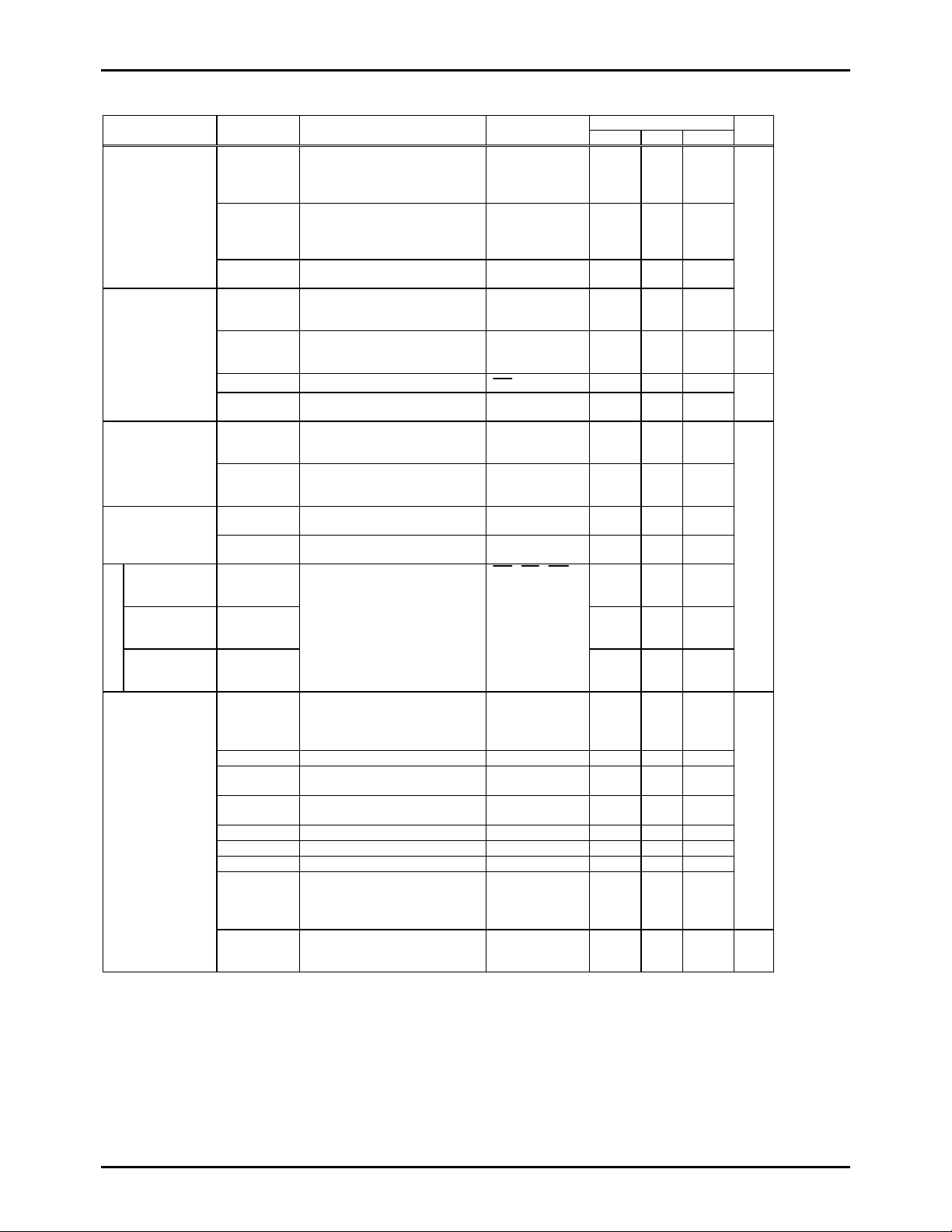
3. Electrical Characteristics at Ta=- 20 to +85°C, VSS=0V, VDD=3.0 to 5.5V (Unless othe r wis e specified)
Parameter Symbol Conditions
Input High le v el
current
Input Low level
current
Output High level
voltage
VOH (2) IOH=-10 µA Ports with the
voltage
Hysteresis
Voltage
High level
threshold
voltage
Low level
threshold
Schmitt characteristics
voltage
urrent consumption
Two-pin RC oscillator
Ceramic osci llator IDDOP (2)
IDDOP (3)
IDDOP (4)
IDDOP (5)
IDDOP (6)
External clock IDDOP (7)
IDDOP (8)
Standby mode IDDst Output N-channel, VDD=6V
IIH(1) Output Nch Tr. OFF
IIH (2) Output Nch Tr. OFF
IIH (3) When external clock is used,
IIL(1) Output Nch Tr. OFF
IIL(2) Output Nch Tr. OFF
IIL(3) VIN=VSS
IIL(4) When external clock is used,
VOH (1) IOH=-50 µA
VOL(1) IOL=10 mA
VOL(2) IOL=1 mA,
VHIS 0.1VDD
VtH 0.4VDD 0.8VDD
VtL
IDDOP (1)
(including OFF leak current
of Nch Tr.)
VIN=+13.5V
(including OFF leak current
of Nch Tr.)
VIN=VDD
VIN=VDD
VIN=VSS
VIN=VSS
VIN=VSS
VDD=4.0 to 6 .0V
VDD=4.0 to 6 .0 V
IOL of each Port : 1 mA or less
Output N-channel transistors are
•
off when operating
Port = VDD
•
Fig. 2, fosc=800 kHz (typical)
•
Fig. 3, 4 MHz, no divider
•
Fig. 3, 4 MHz, divide-by-three
•
circuit
Fig. 3, 4 MHz, divide-by-four
•
circuit
Fig. 3, 400 kHz
•
Fig. 3, 800 kHz
•
384 kHz to 4330 kHz, no divider
•
1152 kHz to 4330 kHz,
•
divide-by-three circuit
1536 kHz to 4330 kHz,
•
divide-by-four circuit
transistor off
Ports=VDD VDD=2.5V
Applicable pins
and notes
Port C and D with
the open-drain
specifications
Port A, E and G
with the
open-drain
specifications
OSC1 1.0
Ports with the
open-drain
specifications
Ports with the
pull-up resistor
specifications
RES
OSC1 -1.0
Ports with the
pull-up resistor
specifications
pull-up resistor
specifications
Port 1.5 Output Low level
Port 0.5
RES, INT, SCK
SI, and schmitt
specification
OSC1
(Note 5)
VDD
VDD 4.0 10
VDD 3.0 8
VDD 3.0 6
VDD 2.0 5
VDD 3.0 6
VDD 4.0 10
VDD 3.0 8
VDD
VDD
5.0
1.0
-1.0
-1.3 -0.35 mA
-45 -10
VDD-1.2 V
VDD-0.5
,
0.2VDD 0.6VDD
0.05
Ratings
min. typ. max.
3.0
0.025
6
10
5
unit
A
µ
A
µ
mA
A
µ
No.6829-13/22
Page 14
LC65F1306A
O
c
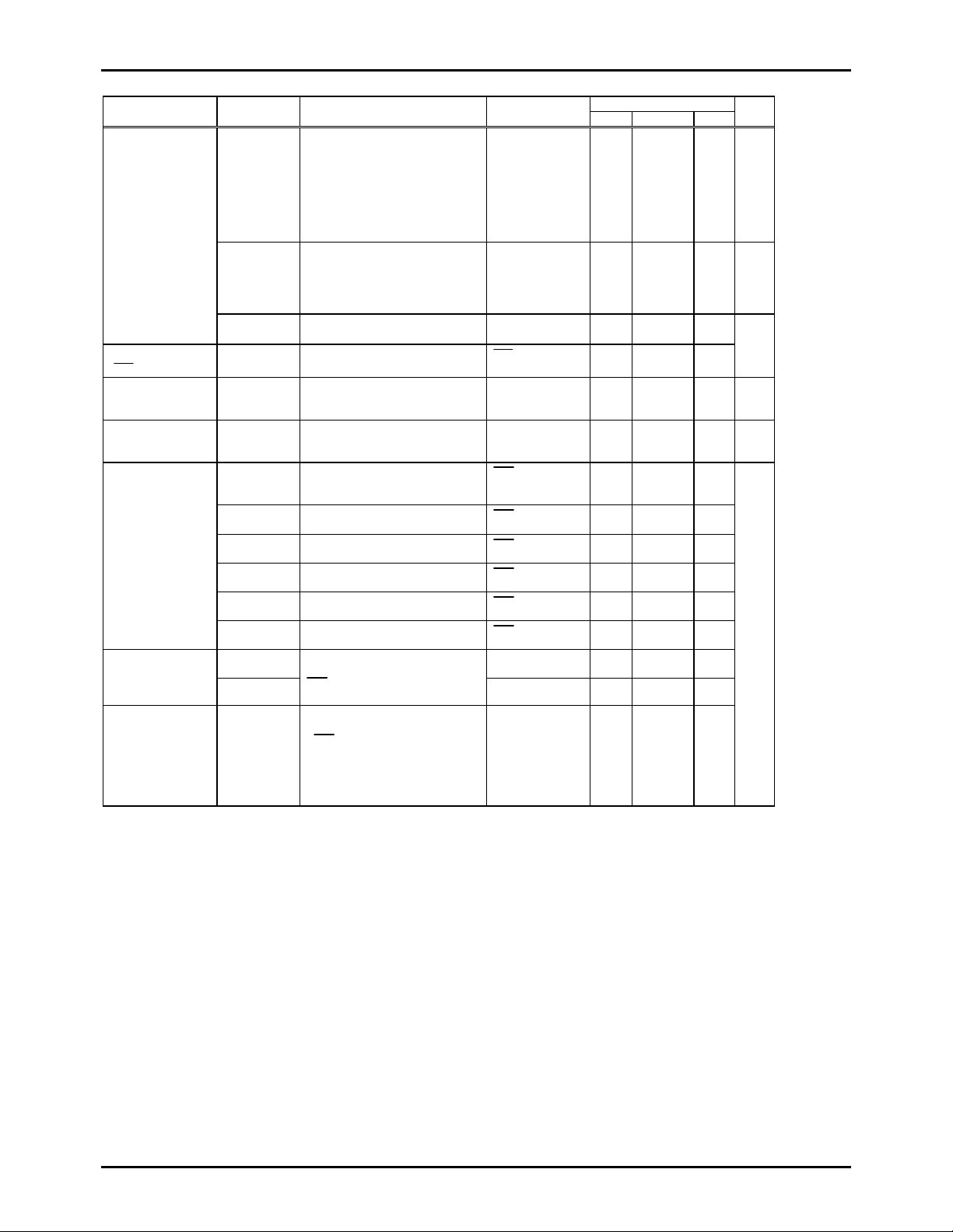
Parameter Symbol Conditions Pin
scillation
haracteristics
Ceramic resonator
Frequency
fCFOSC
(Note 7)
Fig. 3 fo=400kHz
•
Fig. 3 fo=800kHz
•
Fig. 3 f o=1MHz
•
Fig. 3 fo=4MHz, with no divider,
•
OSC1,OSC2
OSC1,OSC2
OSC1,OSC2
OSC1,OSC2
392
784
980
3920
divide-by-three, or divide-by-four
circuit
Oscillation
stabilizing time
(Note 8)
tCFS
Fig. 4 fo=400kHz
•
Fig. 4 fo=800kHz, 1MHz, or
•
4MHz, with no divider,
10
divide-by-three, or divide-by-four
circuit
Two-pin RC
oscillator frequency
Pull-up resistance
RES
External reset
characteristics
Reset time
Pin capacitance Cp f=1MHz,
fMOSC
Fig. 2 Cext=270pF±5%
•
Fig. 2 Rext=5.6k
•
Ω
±
1%
Ru VIN=VSS VDD=5V
tRST
OSC1, OSC2 587 800 1298 kHz
RES
200 500 800
10 pF
Pins except for tested pins,
VIN=VSS
Serial clock
Input clock Cycle
time
Output clock Cycle
tCKCY(1)
tCKCY(2) Fig. 6
time
Input clock low
level pulse width
Output clock low
level pulse width
Input clock high
level pulse width
Output clock high
level pulse width
tCKL(1)
tCKL(2)
tCKH(1)
tCKH(2)
Data setup time
Data hold time
tICK
tCKI
Serial output
Output delay time tCKO
Fig. 6
Fig. 6
Fig. 6
Fig. 6
Fig. 6
Specified for the rising edge of
SCK
Fig. 6
Specified for the falling edge of
•
SCK
Select only Nch OD option, and
•
SCK
SCK
SCK
SCK
SCK
SCK
SI
SI 0.2
SO
2.0
0.6
0.6
0.2
add external 1kΩ resistor and
external 50pF capacitor.
Fig. 6
•
Ratings
min. typ. max.
400
800
1000
4000
408
816
1020
4080
unit
kHz
10
See Fig.5
64×tCYC
(Note 9)
32×tCYC
32×tCYC
Serial input
0.4
ms
kΩ
µ
s
No.6829-14/22
Page 15
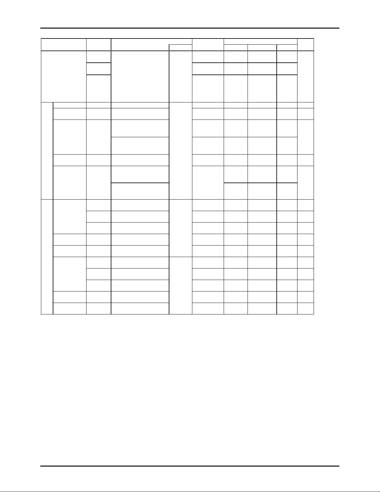
LC65F1306A
Ratings
Parameter Symbol Conditions
Pulse output
Period
High level pulse
width
Low level pulse
width
Resolution 8 bit
Absolute
precision
Conversion
time
Analog input
voltage range
Analog port
input current
A/D converter characteristics
Recommended
constants
(Note 10)
Clear time
(discharge)
Clear period
(charge)
Recommended
constants
(Note 10)
Watch dog timer
Clear time
(discharge)
Clear period
(charge)
tPCY
tPH
tPL
AV+=VDD
TCAD
VAIN AD0 to AD7 VSS VDD V
IAIN
Cw When PE1 is using
Rw When PE1 is using
Rl When PE1 is using
tWCT Fig.8 WDR 100
tWCCY Fig.8
Cw When PE1 is using
Rw When PE1 is using
Rl When PE1 is using
tWCT Fig.8 WDR 10
tWCCY Fig.8
Fig.7
•
TCYC=4 × system clock
•
Select only Nch OD
•
option,
and add external 1kΩ
resistor and external 50pF
capacitor.
AV
=VSS
-
When AD speed is
1/1=26*TCYC
When AD speed is
1/2=51*TCYC
Including the output off
leakage current.
VAIN=VDD
VAIN=VSS
open-drain
open-drain
open-drain
open-drain
open-drain
open-drain
VDD[V]
3 to 5.5
3 to 5.5
3 to 5.5
Applicable
pins and notes
PE0
PE0
PE0
24
47
AD0 to AD7
(The shared
I/O function
ports have
open-drain
specification)
WDR
WDR
WDR
WDR 36 ms
WDR
WDR
WDR
WDR 4.2 ms
min. typ. max.
(TCYC=
0.92µs)
(TCYC=
0.92µs)
1
-1
64×TCYC
32×TCYC
10%
±
32×TCYC
10%
±
1
±
260
510
0.1±5%
680±1%
100±1%
0.01±5%
680±1%
100±1%
2
±
(TCYC=
10µs)
(TCYC=
10µs)
unit
µ
LSB
µ
A
µ
F
µ
kΩ
Ω
µ
F
µ
kΩ
Ω
µ
s
s
s
s
Notes:
(1) When oscillated internally under the oscillating conditions in Fig.3, generated voltage can be over the maximum limit of
the VDD.
(2) Average for 100 ms period.
(3) Operating supply voltage VDD must be held until the microcontroller enters in the standby mode after the execution of the
HALT instruction. Any chattering should not be generated at the PA3 pin during the HALT instruction execution cycle.
(4) Recommended circuit constants that are verified by the oscillator manufacturer, using oscillator characteristic evaluation
board selected by SANYO.
(5) T he OSC1 pin will have schmitt characteristics when external clock oscillator or the two-pin RC oscillator is selected as
an oscillation option.
(6) These are the results of testing using the value at each part on the Fig.3 circuit which is recommended by SANYO. These
results do not include the current applied to the output transistor, nor the current applied to the transistor with a pull-up
resistor on the LSI.
(7) fCFOSC is the frequency when the values in table 1 are used.
(8) This indicates the elapsed time that is required before the oscillation becomes stable after the VDD exceeds the minimum
limit of the operation supply voltage.
(9) TCYC=4×system clock period
(10) When used in an environment that may result in condensation, note that a current leakage between PE1 and adjacent pins
No.6829-15/22
Page 16
LC65F1306A
or a current leakage at external integration circuit using R and C could occur.
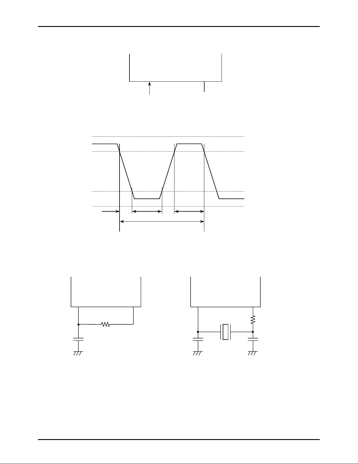
OSC1 (OSC2)
External Clo ck
OPEN
VDD
0.8VDD
0.2VDD
textF
textL
text
textR
textH
VSS
Figure 1 External Clock Input Waveform
OSC2 OSC1
OSC2 OSC1
Cext
Rext
C1 C2
Ceramic
Resonator
R
Figure 2 Two-pin RC Oscillator Circuit Figure 3 Ceramic Resonator Circuit
No.6829-16/22
Page 17
LC65F1306A
f
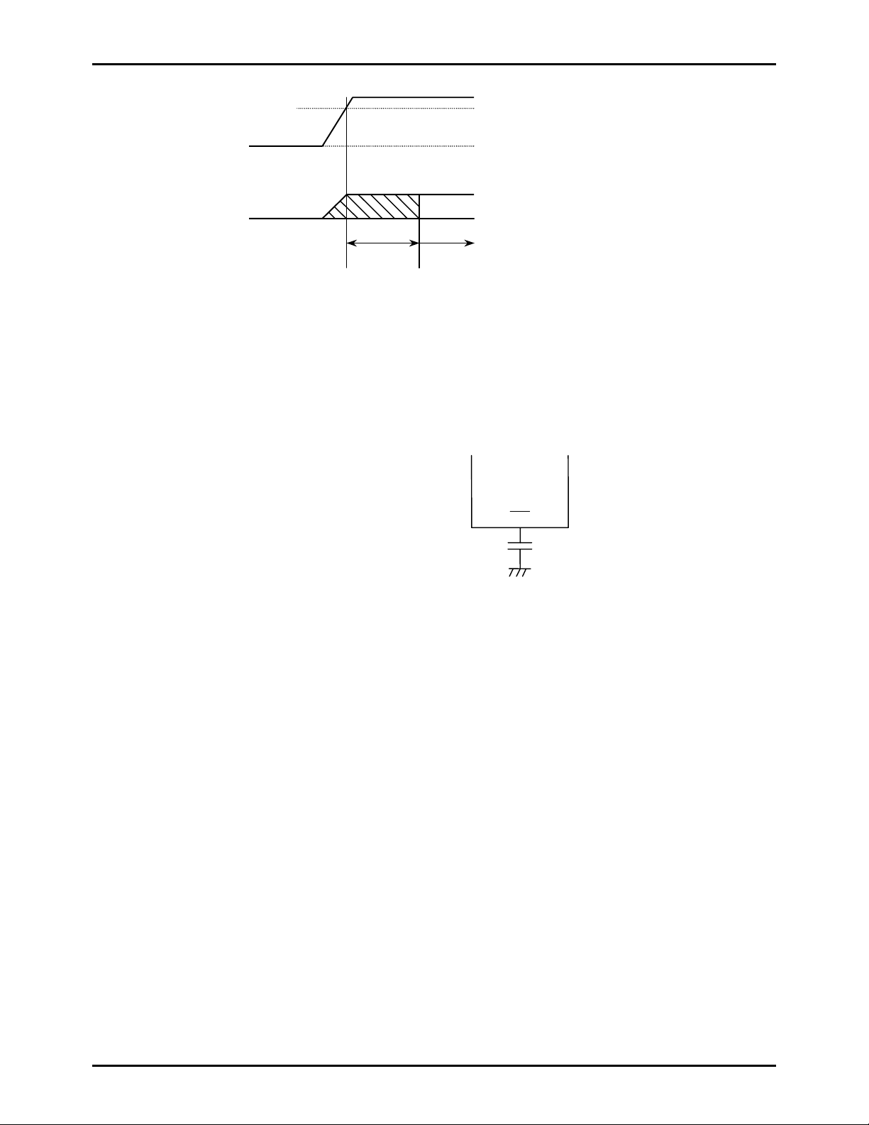
VDD
Oscillation
stabilizing time
Figure 4 Oscil l ation Stabil izing Time
Table 1 Recommended Ceramic Resonator constants
Data will be added once evaluation has been
completed.
tCFS
The lowest limit o
the operating VDD
0V
Stable oscillation
RES
CRES(=0.1 µF)
Figure 5 Reset Circuit
(Note) If measured from the instant the voltage level
reaches the lowest limit of the operating VDD
(i.e. not including the rising time), the reset
time when CRES=0.1 µF is used should be
between 10 ms to 100 ms.
No.6829-17/22
Page 18
LC65F1306A
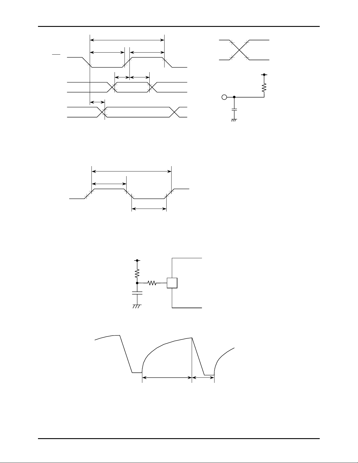
SCK
tCKL tCKH
SI
tCKO
tCKCY
tICK tCKI
Input Data
Load circuit
0.8VDD
0.2VDD
VDD
1kΩ
SO
Output Data
50pF
Figure 6 Serial I/O Timing
tPH
0.7VDD
tPCY
tPL
0.25VDD
The load conditions are
the same as those in
Figure 5.
Figure 7 Port PE0 Pulse Output Timing
Rw
RI
PE1/WDR
Cw
tWCCY tWCT
tWCCY : Charge time made by the external Cw, Rw, and Rl time constants
tWCT : Discharge time made by program control
Figure 8 Watchdog Timer Waveform
No.6829-18/22
Page 19

RC Oscillator Characteristic of LC65F1306A
Data will be added once evaluation has been completed.
LC65F1306A
No.6829-19/22
Page 20
LC65F1306A
Notes on Circuit Board Design
This section provides hints and countermeasure for noise problem in terms of microcontroller when designing circuit boards
using these microcontrollers for a mass production. These design techniques are effective to prevent and avoid the defects (e.g.
malfunctions of the microcontroller or a runaway program) caused by noise.
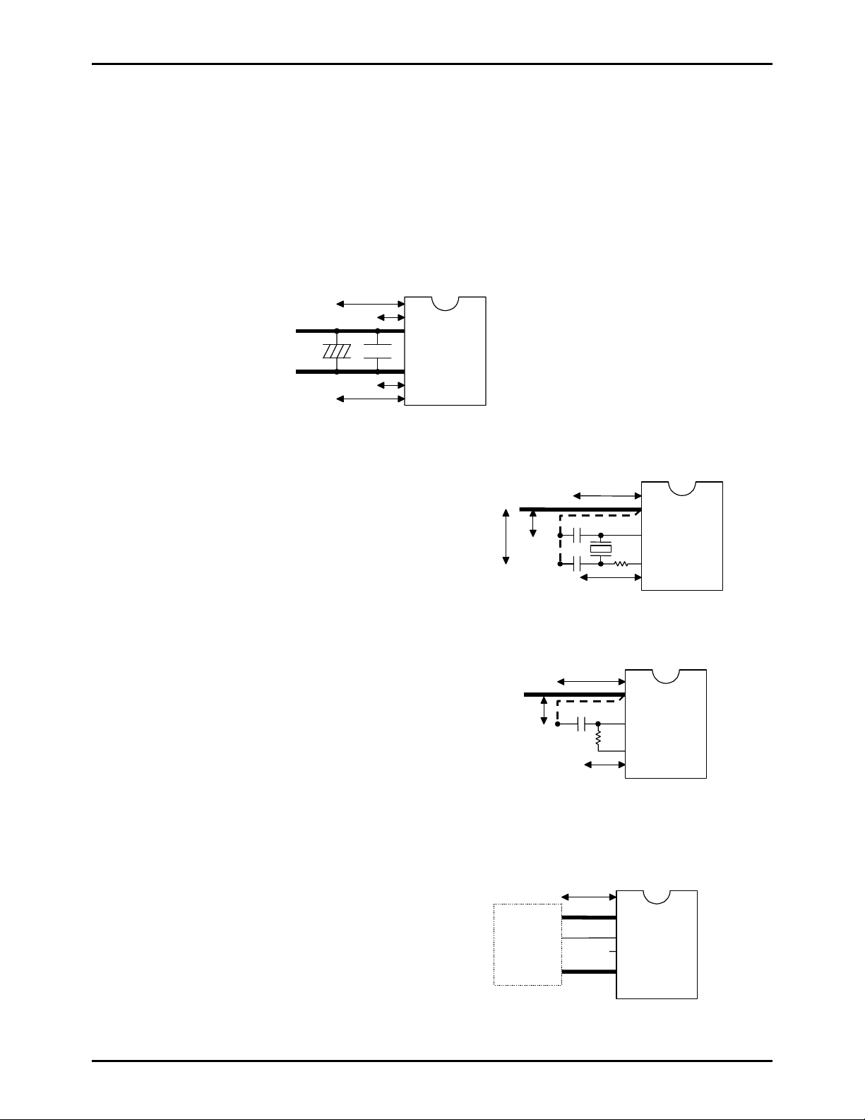
1. VDD, VSS : Power Supply Pins
Add capacitors between the VDD and VSS pins so that they meet the following conditions.
The length of the line from the VDD to the two capacitors and the length of the line from the VSS to the two capacitors
•
should be as equal as possible (L1=L1’, L2=L2’), and should be as short as possible.
Add the larger capacitor to ‘C1’ position and smaller capacitor to ‘C2’ position.
•
The VDD and VSS lines on the circuit board should be thicker than any other lines.
C1 C2
2. OSC1, OSC2 : Clock I/O Pins
• When the ceramic resonator option is selected : ( Figure 2-1)
The length of the lines (Losc in Fig.2-1) between the clock I/O
•
pins (input: OSC1, output: OSC2) and the external components
should be as short as possible.
• The length of the lines (Lvss+L1 or L2 ) between each capacitor
and the VSS pin should be as short as possible.
The VSS line for the oscillation circuit and the VSS line for other
•
functions should be branched as close as possible to the
microcontroller's VSS pin.
• Oscillation constants written in this specification sheet (such as the
capacitor C1, C2 and the damping resistor Rd) may have to be
changed and the frequency should be adjusted, depending on the
pattern capacity of the circuit board. In this case, contact the
oscillator manufacturer about it.
• When two- pin RC oscillator option is selected: (Figure 2-2)
• The length of the lines (Losc) between the clock I/O pins (input:
OSC1, output: OSC2) and the external components (capacitor
Cext, resistor Rext) should be as short a s p ossi ble.
The length of the line (Lvss+Lc) between the capacitor and the
•
VSS pin should be as short as possible.
The VSS line fo r the o scillat ion cir cuit an d the VS S line for o ther
•
functions should be branched as close as possible to the
microcontroller's VSS pin.
• When the external oscillation option is selected: (Figure 2-3)
The length of the line (Losc) between the clock input pin (OSC1)
•
and the external oscillator should be as short as possible.
The clock output pin (OSC2) should be opened.
•
• The length of the line between the VSS and the external oscillator,
and the length of the line between the VDD and the external
oscillator should be as short as possible.
L2
L1
VSS
+
VDD
L1'
L2
'
L2
C1
C2
Lvss
Losc
L1
Rd
VSS
OSC1
OSC2
Figure 2-1. Sample Oscillation Circuit 1
(Ceramic resonator)
Lvss
Lc
Cext
VSS
OSC1
Rext
OSC2
Losc
Figure 2-2. Sample Oscillation Circuit 2
(Two-pin RC Oscillator)
Losc
VSS
External
Oscillator
OPEN
OSC1
OSC2
VDD
Figure 2-3. Sample Oscillation Circuit 3
(External Oscillator)
No.6829-20/22
Page 21
LC65F1306A
A
A
• Other note on all oscillator circuit:
Place the lines for signals that can easily change suddenly, high amplitude signals connected to the higher capacity voltage
•
(+15 V) ports, and powerful current supplies as far as possible from the oscillation circuit, and do not cross these lines
with lines concerned to the clock.
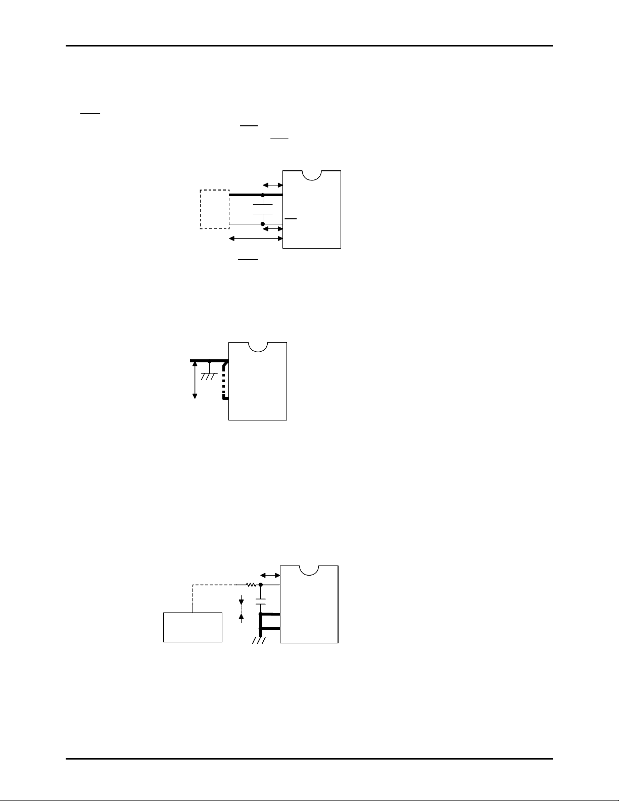
3.
: Reset Pin
RES
The length of line (Lres) between the
•
RES
• The length of lines (L1 and L2) between the
pin and the external circuit should be as short as possible.
pin and the capacitor (Cres), and the VSS and the capacitor should
RES
be as short as possible.
External
Circuit
Cres
Lres
L2
L1
VSS
RES
Figure 3.
Pin Patterns
RES
4. TEST : Test Pin
• The length of line (L) between the VSS and the TEST pin should be as short as possible.
The TEST pin and the VSS pin should be connected as close as possible to the VSS pin.
•
L
VSS
TEST
Figure 4. Test Pin Patterns
5. AD0 to AD7 : Analog Input Pins
The connection for the analog input pins, such as A/D converter input pins and comparator input pin, should meet the
following conditions.
The length of the line (L1) between the damping resistor (R1) and each analog pins should be as short as possible.
•
• The capacitor added between each analog pins and AV- pin (base voltage input pin for A/D converter) should be located
as close as possible to the AV- input pin.
External circuit
(sensor block)
Figure 5. Analog Input Pins Pa tterns
Rl
L1
D4-7
C
L2
Input Pins
Analog
D3-0
AVVSS
6. I/O Pins
All I/O pins on these microcontrollers have function of both input and output.
When used as an input pin, add a damping resistor and keep the length of the line to that pin as short as possible.
•
No.6829-21/22
Page 22
LC65F1306A
[Supplement]
In addition to the techniques for designing a circuit board, the following options and programming are effective to
prevent and avoid the defects (the malfunction or a runaway program).
If signals are input from external sources when the microcontroller power supply is unstable, select the higher
•
capacity voltage (N-channel open drain) output type for the input pin, and add a damping resistor close to the
pin.
When the external signals are input to pins, the chattering of the key must be removed.
•
• The data should be output periodically from the pins using the output instruction (OP or SPB).
To read the data input to the I/O common pins, the output value should be set to ‘1’ using the output instruction
•
(OP or SPB).
7. Unused Pins
See the user’s manual for each microcontrollers or the final edition of the specification sheet.
•
No.6829-22/22
PS
 Loading...