

Page 1

CMOS LSI
Ordering number : EN*5117
92995HA (OT) No. 5117-1/39
Preliminary
SANYO Electric Co.,Ltd. Semiconductor Bussiness Headquarters
TOKYO OFFICE Tokyo Bldg., 1-10, 1 Chome, Ueno, Taito-ku, TOKYO, 110-8534 JAPAN
4-Bit Microcomputer
for Small-Scale Control Applications
LC6529N, LC6529F, LC6529L
Overview
The LC6529N/F/L provides the basic architecture and
instruction set of the Sanyo LC6500 Series of 4-bit singlechip microcomputers in a version specially for small-scale
control applications involving circuits built with standard
logic elements, applications using simple, comparatorbased voltage or phase detectors, or other applications
controlling a limited number of controls. The LC6529F is
a replacement for the former LC6529H. (Certain functions
differ, however.) The N (medium-speed) and L (powersaving) versions are new additions to the lineup.
Features
• Power-saving CMOS design (Standby mode accessed
with HALT instruction included.)
• Memory: 1 kilobyte of 8-bit ROM and 64 words of 4-bit
RAM
• Instruction set: 51-member subset of LC6500 standard
complement of 80 instructions
• (L version) Wide range of operating voltages:
2.2 to 6.0 V
• (F version) 0.92 µs/3.0 V instruction cycle time
• Flexible I/O ports
Four ports with up to 16 lines
— Bidirectional I/O ports: 12
Dedicated input ports: 4 (These double as
comparator inputs.)
— I/O voltage limit: max. +15 V (open-drain
configuration)
— Output current: max. 20 mA sink current (capable of
directly driving an LED)
Choice of options to match system specifications
— Choice of open-drain or pull-up resistor output
configurations at the bit level for all ports
— Choice of reset output levels for Ports C and D in
groups of 4 bits each
Port E configurable as four comparator inputs
• Stack: Four levels
• Timers: 4-bit prescaler plus 8-bit programmable counter
• Comparators: 4 channels (2 reference levels)
Separator reference level for each channel pair
— Feedback resistor option for choice of input with or
without hysteresis
• Choice of clock oscillator options to match system
specifications
— Oscillator circuit options: 2-pin RC oscillator circuit
(N and L versions) or 2-pin ceramic oscillator circuit
(N, F, and L versions)
— Frequency divider options: Built-in 1/3 and 1/4
frequency dividers that eliminate the need for
external frequency dividers
Page 2
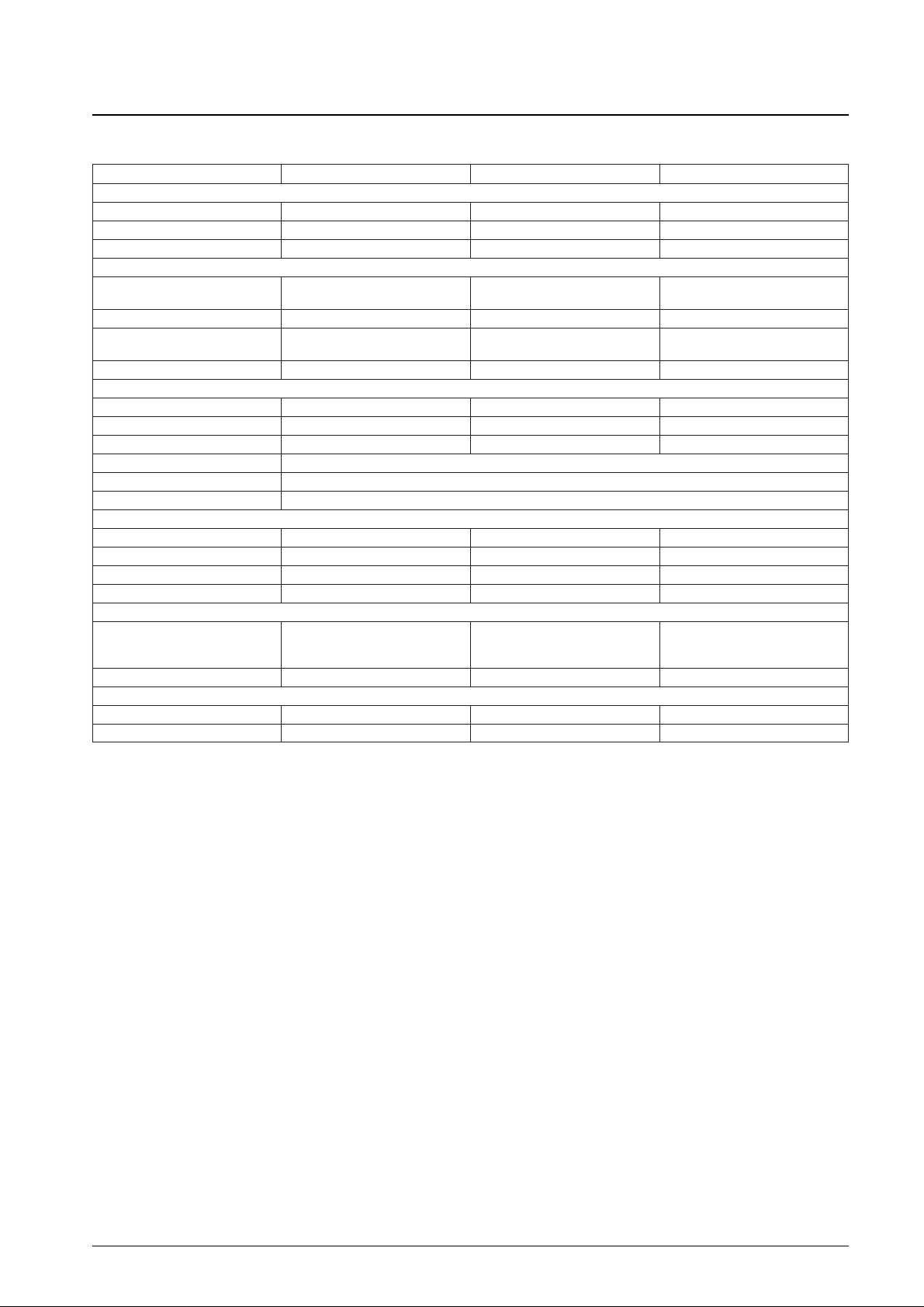
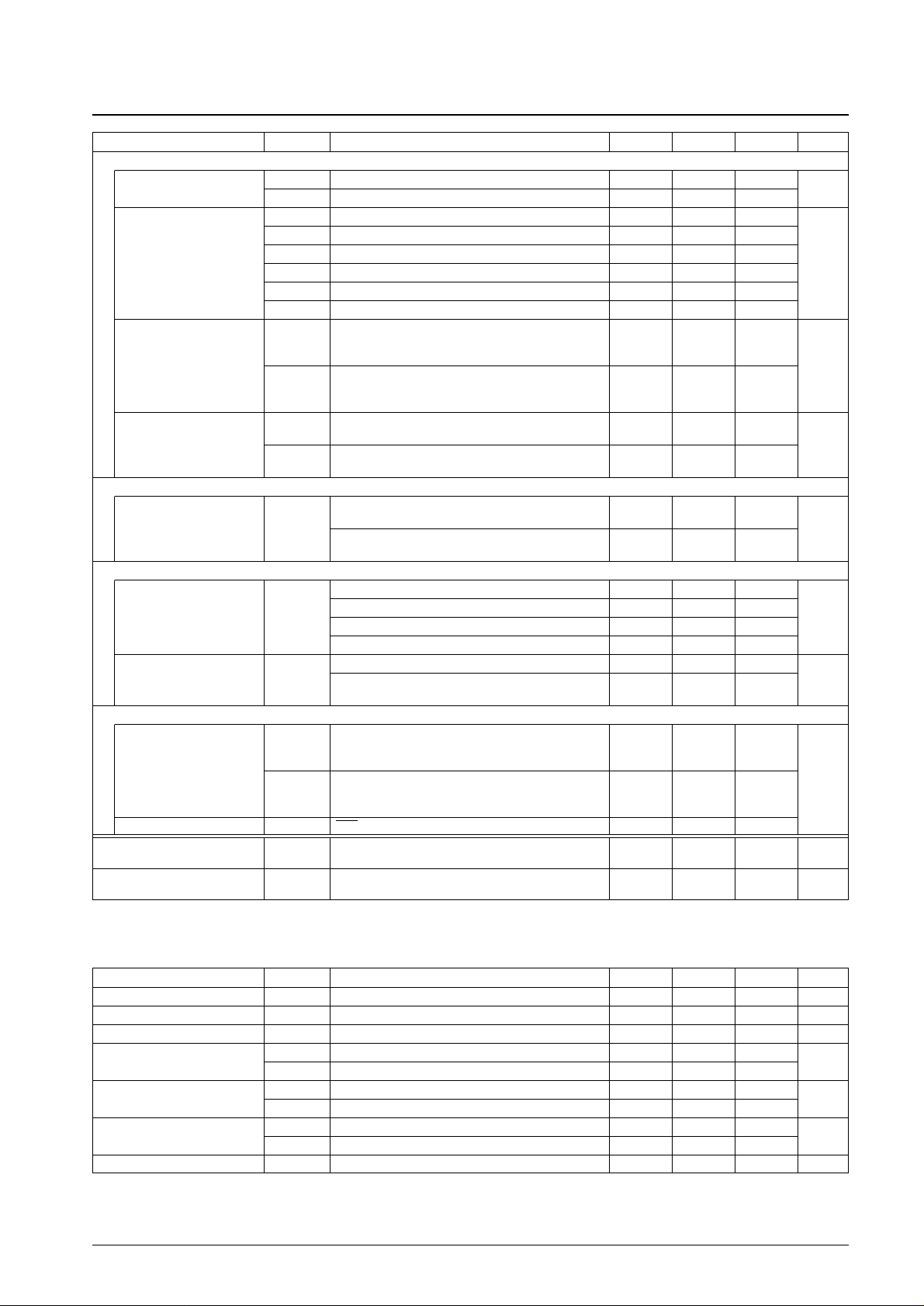
Summary of Functions
Note: The oscillator constants will be announced once the recommended circuit design has been decided.
No. 5117-2/39
LC6529N, LC6529F, LC6529L
Item LC6529N LC6529F LC6529L
[Memory]
ROM 1024
× 8 bits 1024 × 8 bits 1024 × 8 bits
RAM 64 × 4 bits 64 × 4 bits 64 × 4 bits
Instruction set 51 51 51
[On-board functions]
Timers
4-bit prescaler plus 8-bit 4-bit prescaler plus 8-bit 4-bit prescaler plus 8-bit
programmable counter programmable counter programmable counter
Stack levels 4 4 4
Standby mode
HALT instruction places chip HALT instruction places chip HALT instruction places chip
on standby. on standby. on standby.
Comparators 4 channels (2 reference levels) 4 channels (2 reference levels) 4 channels (2 reference levels)
[I/O ports]
Number of ports 12 bidirectional I/O pins, 4 input pins 12 bidirectional I/O pins, 4 input pins 12 bidirectional I/O pins, 4 input pins
I/O voltage limit max. 15 V (ports A, C, and D) max. 15 V (ports A, C, and D) max. 15 V (ports A, C, and D)
Output current 10 mA typ. 20 mA max. 10 mA typ. 20 mA max. 10 mA typ. 20 mA max.
I/O circuit configuration Choice of open-drain output or pull-up resistors at the bit level for ports A, C, and D
Reset output level Choice of high or low in groups of 4 bits each (ports C and D)
Port function Port E configurable as four comparator inputs
[Characteristics]
Minimum cycle time 2.77 µs (V
DD
≥ 3.0 V) 0.92 µs (VDD≥ 3.0 V) 3.84 µs (VDD≥ 2.2 V)
Operating temperature –40 to +85°C –40 to +85°C –40 to +85°C
Power supply voltage 3.0 to 6.0 V 3.0 to 6.0 V 2.2 to 6.0 V
Current drain 1.1 mA typ. 1.6 mA typ. 1.0 mA typ.
[Clock]
RC (850 kHz, 400 kHz typ.) RC (400 kHz typ.)
Oscillator Ceramic oscillator (400 kHz, 800 kHz, Ceramic oscillator (2 MHz, 4 MHz) Ceramic oscillator (400 kHz, 800 kHz,
2 MHz, 4 MHz) 2 MHz, 4 MHz)
Frequency divider options 1/1, 1/3, 1/4 1/1 1/1, 1/3, 1/4
[Miscellaneous]
Package DIP24S, SSOP24, MFP30S DIP24S, SSOP24, MFP30S DIP24S, SSOP24, MFP30S
OTP Included Included Included
Page 3
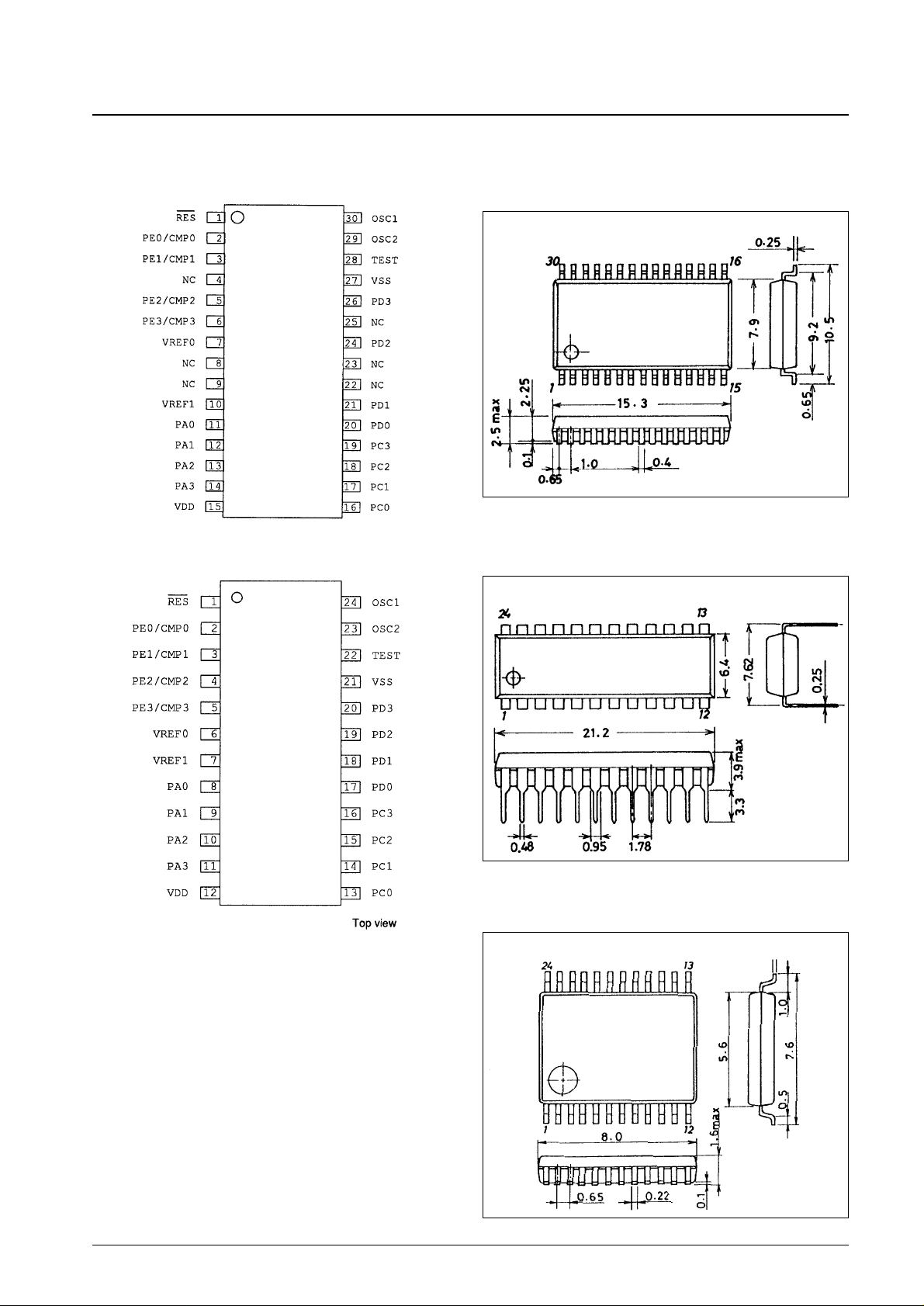
Pin Assignments
MFP30S
DIP24S/SSOP24
Note: Do not use dip-soldering when mounting the SSOP package on the
circuit board.
Package Dimensions
unit: mm
3073A-MFP30S
No. 5117-3/39
LC6529N, LC6529F, LC6529L
SANYO: MFP30S
[LC6529N, 6529F, 6529L]
unit: mm
3067-DIP24S
SANYO: DIP24S
[LC6529N, 6529F, 6529L]
unit: mm
3175A-SSOP24
SANYO: SSOP24
[LC6529N, 6529F, 6529L]
Note: The above diagrams give only the nominal dimensions. Contact Sanyo for drawings complete with tolerances.
Page 4
Pin Names
OSC1, OSC2: Pins for RC or ceramic oscillator circuit
TEST: Test pin
RES: Reset pin
PA0 to PA3: Bidirectional I/O port A, bits 0 to 3
PC0 to PC3: Bidirectional I/O port C, bits 0 to 3
PD0 to PD3: Bidirectional I/O port D, bits 0 to 3
PE0 to PE3: Unidirectional input port E, bits 0 to 3
CMP0 to CMP3: Comparator input port, bits 0 to 3
VREF0, VREF1: Reference inputs
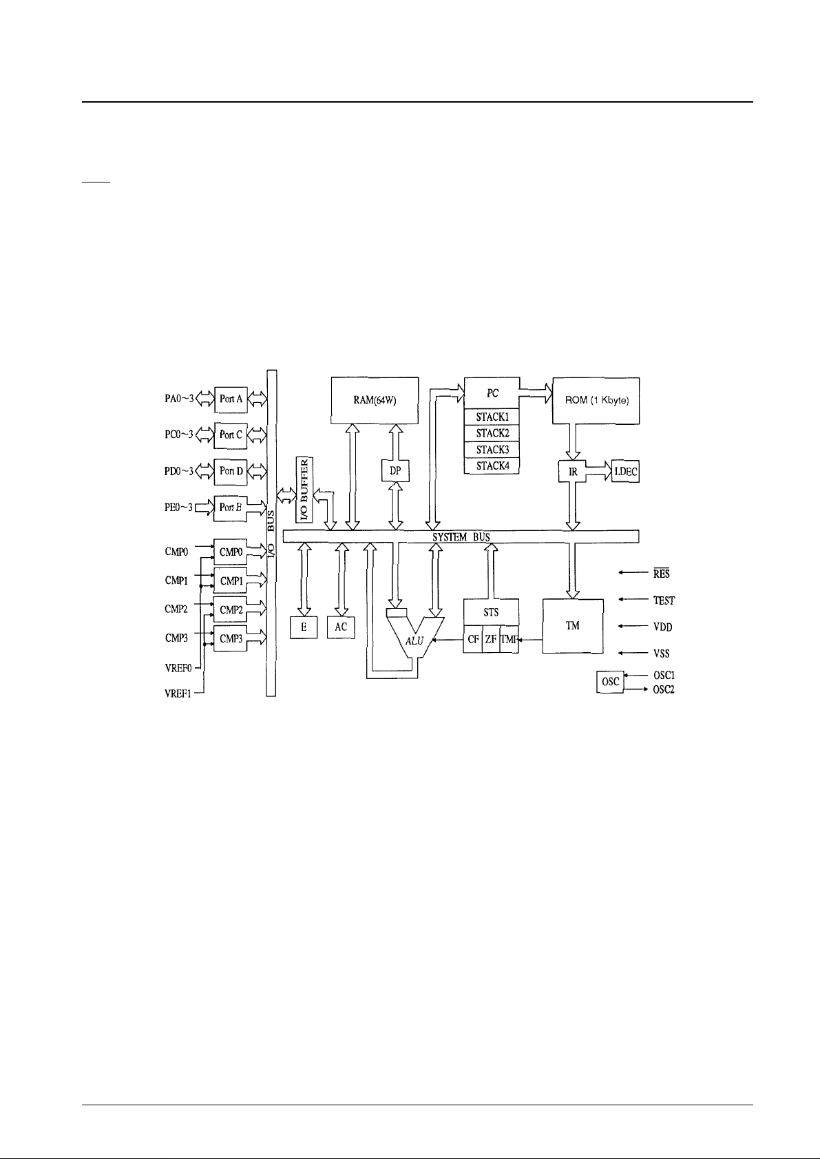
System Block Diagram
RAM: Data memory ROM: Program memory
AC: Accumulator PC: Program Counter
ALU: Arithmetic and Logic Unit IR: Instruction Register
DP: Data pointer I.DEC: Instruction Decoder
E: E register CF: Carry Flag
OSC: Oscillator circuit ZF: Zero Flag
TM: Timer TMF: Timer overflow Flag
STS: Status register
No. 5117-4/39
LC6529N, LC6529F, LC6529L
Page 5

Pin Functions
No. 5117-5/39
LC6529N, LC6529F, LC6529L
Pin No. Symbol I/O Function Output driver type Options State after reset
V
DD
V
SS
OSC1
OSC2
PA0
PA1
PA2
PA3
PC0
PC1
PC2
PC3
PD0
PD1
PD2
PD3
PE0/CMP0
PE1/CMP1
PE2/CMP2
PE3/CMP3
V
REF
0
V
REF
1
RES
TEST
—
—
I
O
I/O
I/O
I/O
I
I
I
I
I
Power supply. Normally +5 V.
Power supply. 0 V.
Pins for attaching external system
clock oscillator circuit (RC or ceramic)
• Bidirectional I/O port A0 to A3: 4-bit
input (IP instruction), 4-bit output (OP
instruction), 1-bit conditionals (BP
and BNP instructions), 1-bit set and
reset (SPB and RPB instructions)
• PA3 also doubles as standby
operation control.
• Block chattering from entering PA3
during the HALT instruction
execution cycle.
• Bidirectional I/O port C0 to C3.
Functions the same as PA0 to PA3
except that there is no the standby
operation control.
• Option controls whether output is
high or low after reset.
Bidirectional I/O port D0 to D3.
Functions and options the same as
PC0 to PC3.
• When configured for comparator
input: CMP0 and CMP1 use
reference voltage V
REF
0; CMP2 and
CMP3 use reference voltage V
REF
1.
• 4-bit (CMP0 to 3) input (IP
instruction)
• 1-bit conditionals (BP and BNP
instructions)
• When configured for port E input:
• 4-bit (E0-3) input (IP instruction)
• 1-bit conditionals (BP and BNP
instructions)
• Comparator reference level inputs:
CMP0 and CMP1 use reference
voltage V
REF
0; CMP2 and CMP3
use reference voltage V
REF
1.
• Connect to V
SS
when PE0/CMP0 to
PE3/CMP3 configured as port E.
• System reset input
• Connect external capacitor for power
up reset.
• Low level input for a minimum of four
clock cycles triggers a reset.
Chip test pin. Normally connect to V
SS
.
• N channel: sink
current type
• I/O voltage limit for
open-drain
configuration: max.
+15 V
• P channel: highimpedance pull-up
type
• N channel: sink
current type
• I/O voltage limit for
open-drain
configuration: max.
+15 V
• P channel: lowimpedance pull-up
type
• N channel: sink
current type
• I/O voltage limit for
open-drain
configuration: max.
+15 V
• P channel: highimpedance pull-up
type
1
1
1
1
4
4
4
4
4
2
1
1
—
—
High output (output
N channel transistor
off)
High or low (option)
High or low (option)
—
—
1. 2-pin RC oscillator circuit
(1-pin external clock)
2. 2-pin ceramic oscillator circuit
3. Frequency divider options:
1/1, 1/3, 1/4
1. Open-drain output
2. Pull-up resistor
• Choice of configuration 1. or 2. at
bit level
1. Open-drain output
2. Pull-up resistor
3. High output after reset
4. Low output after reset
• Choice of configuration 1. or 2. at
bit level
• Choice of configuration 3. or 4. at
port (4-bit) level
1. Open-drain output
2. Pull-up resistor
3. High output after reset
4. Low output after reset
• Choice of configuration 1. or 2. at
bit level
• Choice of configuration 3. or 4. at
port (4-bit) level
1. Comparator input
2. Port E input
3. Without feedback resistor
4. With feedback resistor
• Choice of configuration 1. or 2. at
port (4-bit) level
• Options 3. and 4. only available
with 1.
Page 6
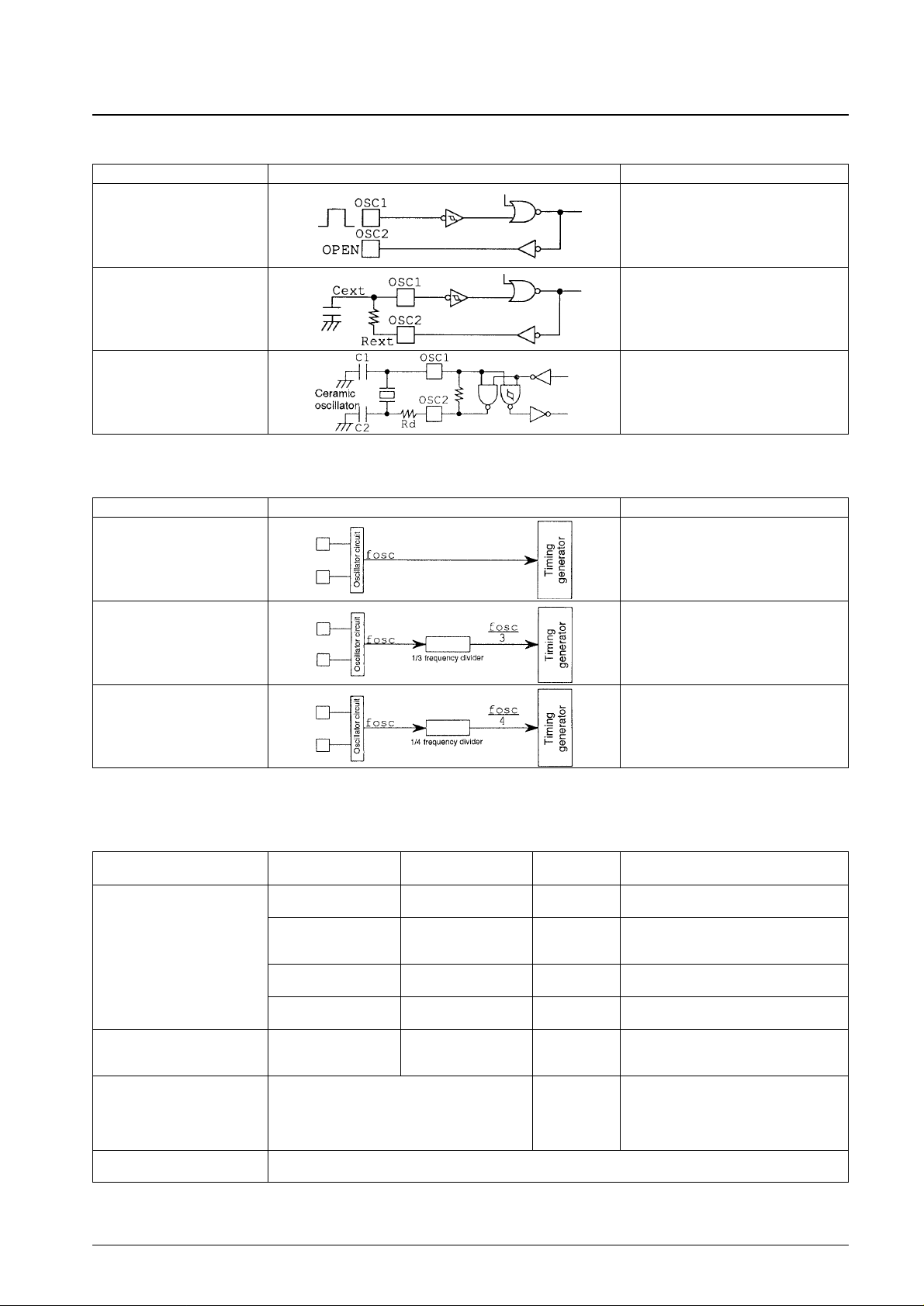
Oscillator Circuit Options
Frequency Divider Options
Frequency Divider Options
LC6529N
No. 5117-6/39
LC6529N, LC6529F, LC6529L
Name Circuit diagram Conditions, etc.
External clock
2-pin RC oscillator circuit
2-pin ceramic oscillator circuit
Leave OSC2 open.
Name Circuit diagram Conditions, etc.
No frequency divider (1/1)
1/3 frequency divider
1/4 frequency divider
Available with all three oscillator circuit options
(N, F, and L versions)
Available only with external clock and ceramic
oscillator circuit options (N and L versions)
Available only with external clock and ceramic
oscillator circuit options (N and L versions)
Oscillator circuit Frequency
Frequency divider options
VDDrange Note
(cycle time)
400 kHz 1/1 (10 µs) 3 to 6 V
1/3 and 1/4 frequency divider options
not available
1/1 (5 µs) 3 to 6 V
800 kHz 1/3 (15 µs) 3 to 6 V
Ceramic oscillator
1/4 (20 µs) 3 to 6 V
2 MHz
1/3 (6 µs) 3 to 6 V
1/1 frequency divider option not available
1/4 (8 µs) 3 to 6 V
4 MHz
1/3 (3 µs) 3 to 6 V
1/1 frequency divider option not available
1/4 (4 µs) 3 to 6 V
External clock based on RC
200 k to 1444 kHz 1/1 (20 to 2.77 µs) 3 to 6 V
oscillator circuit
600 k to 4330 kHz 1/3 (20 to 2.77 µs) 3 to 6 V
800 k to 4330 kHz 1/4 (20 to 3.70 µs) 3 to 6 V
Use 1/1 frequency divider and recommended
constants or, if this is not possible, one of the
RC oscillator circuit frequency, frequency divider option, and V
DD
range 3 to 6 V
combinations listed for external clocks based on
an RC oscillator circuit.
External clock based on ceramic
This configuration not allowed. Use an external clock based on an RC oscillator circuit instead.
oscillator circuit
Page 7
LC6529F
LC6529L
Reset Level Options for Ports C and D
The following two options are available for controlling the output levels of ports C and D in groups of four bits each.
Comparator vs. Port E Configuration Option
The four pins PE0/CMP0 to PE3/CMP3 may be configured for comparator input or as port E.
No. 5117-7/39
LC6529N, LC6529F, LC6529L
Oscillator circuit Frequency
Frequency divider options
VDDrange Note
(cycle time)
Ceramic oscillator 4 MHz 1/1 (1 µs) 3 to 6 V
External clock based on RC
200 k to 4330 kHz 1/1 (20 to 0.92 µs) 3 to 6 V
oscillator circuit
External clock based on ceramic
This configuration not allowed. Use an external clock based on an RC oscillator circuit instead.
oscillator circuit
Oscillator circuit Frequency
Frequency divider options
VDDrange Note
(cycle time)
400 kHz 1/1 (10 µs) 2.2 to 6 V
1/3 and 1/4 frequency divider options
not available
1/1 (5 µs) 2.2 to 6 V
800 kHz 1/3 (15 µs) 2.2 to 6 V
Ceramic oscillator
1/4 (20 µs) 2.2 to 6 V
2 MHz
1/3 (6 µs) 2.2 to 6 V
1/1 frequency divider option not available
1/4 (8 µs) 2.2 to 6 V
4 MHz 1/4 (4 µs) 2.2 to 6 V
1/1 and 1/3 frequency divider options not
available
External clock based on RC
200 k to 1040 kHz 1/1 (20 to 3.84 µs) 2.2 to 6 V
oscillator circuit
600 k to 3120 kHz 1/3 (20 to 3.84 µs) 2.2 to 6 V
800 k to 4160 kHz 1/4 (20 to 3.84 µs) 2.2 to 6 V
Use 1/1 frequency divider and recommended
constants or, if this is not possible, one of the
RC oscillator circuit frequency, frequency divider option, and V
DD
range 2.2 to 6 V
combinations listed for external clocks based on
an RC oscillator circuit.
External clock based on ceramic
This configuration not allowed. Use an external clock based on an RC oscillator circuit instead.
oscillator circuit
Option Conditions, etc.
High level output after reset Selection affects all bits of port
Low level output after reset Selection affects all bits of port
Option Conditions, etc.
Comparator input Selection affects all bits of port
Port E input Selection affects all bits of port
Page 8
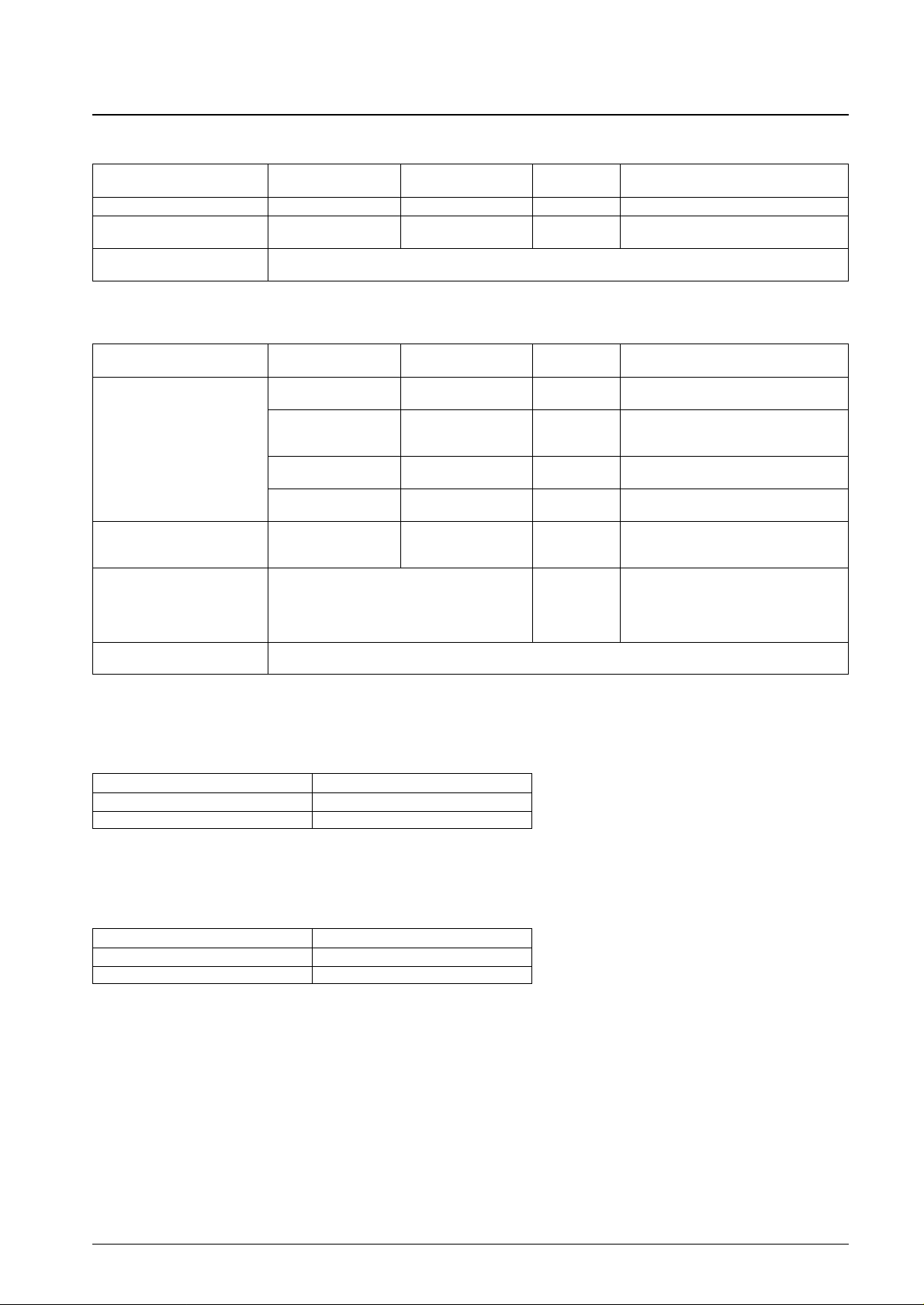
Comparator Options
The comparators offer the following two configuration options.
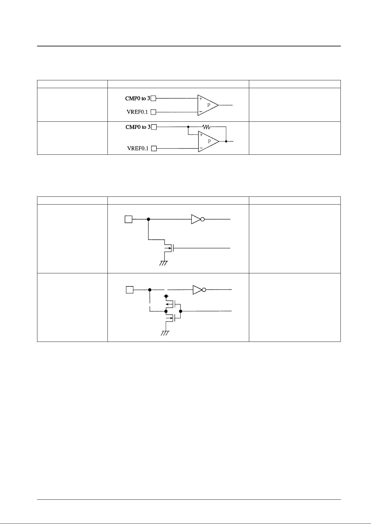
Port Output Configurations
The bidirectional I/O ports A, C, and D offer a choice of two output configurations.
No. 5117-8/39
LC6529N, LC6529F, LC6529L
Name Circuit diagram Conditions, etc.
Without feedback resistor
With feedback resistor
The comparator does not use hysteresis.
The comparator, in combination with an
external resistor, uses hysteresis.
Name Circuit diagram Conditions, etc.
Open drain (OD)
With pull-up resistors (PU)
This option adds a high-impedance pull-up
resistor for port A or D and a low-impedance
one for port C.
Page 9
Specifications
LC6529N
Absolute Maximum Ratings at Ta = 25°C, VSS= 0 V
Note: 1. When the oscillator circuit in Figure 3 and the guaranteed constant are used, this is guaranteed over the full amplitude.
2. Averaged over 100-ms interval.
Allowable Operating Ranges at Ta = –40 to +85°C, VSS= 0 V, VDD= 3.0 to 6.0 V
Note: * Maintain the power supply voltage at VDDuntil the HALT instruction has completed execution, placing the chip in the standby mode. Block
chattering from entering PA3 during the HALT instruction execution cycle.
No. 5117-9/39
LC6529N, LC6529F, LC6529L
Parameter Symbol Conditions min typ max Unit
Maximum supply voltage V
DD
max V
DD
–0.3 +7.0 V
V
I
1 OSC1
*1
–0.3 VDD+ 0.3
Input voltage V
I
2 TEST, RES –0.3 VDD+ 0.3 V
V
I
3 Port E (PE) configuration –0.3 VDD+ 0.3
Output voltage V
O
OSC2 Voltages up to that generated allowed. V
I/O voltages
V
IO
1 Open-drain (OD) configuration –0.3 +15
V
V
IO
2 Pull-up (PU) resistor configuration –0.3 VDD+ 0.3
Peak output current I
OP
PA, PC, PD –2 +20 mA
I
OA
PA, PC, PD: Average for pin over 100-ms interval –2 +20
Average output current
ΣI
OA
1 PA: Total current for pins PA0 to PA3
*2
–6 +40
mA
ΣI
OA
2
PC, PD: Total current for pins PC0 to PC3 and
–14 +90
PD0 to PD3
*2
Pd max1 Ta = –40 to +85°C (DIP24S) 360
Allowable power dissipation Pd max2 Ta = –40 to +85°C (SSOP24) 165 mW
Pd max3 Ta = –40 to +85°C (MFP30S) 150
Operating temperature Topr –40 +85
°C
Storage temperature Tstg –55 +125
Parameter Symbol Conditions min typ max Unit
Supply voltage V
DD
V
DD
3.0 6.0 V
Standby voltage V
ST
VDD: Preserves contents of RAM and registers*. 1.8 6.0 V
V
IH
1
Open-drain (OD) configuration: With output N-channel
0.7 V
DD
13.5
transistor off
VIH2
Pull-up (PU) resistor configuration: With output
0.7 V
DD
V
DD
Input high level voltage
N-channel transistor off
V
V
IH
3 PE: Using port E configuration 0.7 V
DD
V
DD
VIH4 RES: VDD= 1.8 to 6 V 0.8 V
DD
V
DD
VIH5 OSC1: Using external clock option 0.8 V
DD
V
DD
VIL1
PA, PC, PD: With output N-channel transistor off,
V
SS
0.3 V
DD
VDD= 4 to 6 V
V
IL
2 PA, PC, PD: With output N-channel transistor off V
SS
0.25 V
DD
VIL3 PE: Using port E configuration, VDD= 4 to 6 V V
SS
0.3 V
DD
VIL4 PE: Using port E configuration V
SS
0.25 V
DD
Input low level voltage
V
IL
5 OSC1: Using external clock option, VDD= 4 to 6 V V
SS
0.25 V
DD
V
VIL6 OSC1: Using external clock option V
SS
0.2 V
DD
VIL7 TEST: VDD= 4 to 6 V V
SS
0.3 V
DD
VIL8 TEST V
SS
0.25 V
DD
VIL9 RES: VDD= 4 to 6 V V
SS
0.25 V
DD
VIL10 RES V
SS
0.2 V
DD
Operating frequency fop Using the built-in 1/3 or 1/4 frequency dividers extends
200 (20) 1444 (2.77) kHz (µs)
(cycle time) (Tcyc) the maximum to 4.33 MHz.
Continued on next page.
Page 10
Continued from preceding page.
Electrical Characteristics at Ta = –40 to +85°C, VSS= 0 V, VDD= 3.0 to 6.0 V
Note: * The RC oscillator and external clock options require a Schmidt trigger configuration for OSC1.
No. 5117-10/39
LC6529N, LC6529F, LC6529L
Parameter Symbol Conditions min typ max Unit
[External clock conditions]
Frequency text 200 4330 kHz
Pulse width textH, textL 69
ns
Rise/fall times textR, textF 50
[Oscillator guaranteed constants]
Cext OSC1, OSC2: V
DD
= 4 to 6 V, Figure 2 220 ± 5%
pF
2-pin RC oscillator circuit
Cext OSC1, OSC2: Figure 2 220 ± 5%
Rext OSC1, OSC2: V
DD
= 4 to 6 V, Figure 2 4.7 ± 1%
kΩ
Rext OSC1, OSC2: Figure 2 12.0 ± 1%
Ceramic oscillator Figure 3 See Table 1.
OSC1: If the clock frequency exceeds 1.444 MHz, use
the built-in 1/3 or 1/4 frequency divider. Figure 1
Parameter Symbol Conditions min typ max Unit
Open-drain (OD) configuration for port: With output
IIH1 N-channel transistor off. (Includes transistor’s leak 5.0
Input high level current
current.) V
IN
= 13.5 V
µA
I
IH
2 PE: Using port E configuration, VIN= V
DD
1.0
I
IH
3 OSC1: Using external clock option, VIN= V
DD
1.0
Open-drain (OD) configuration for port: With output
IIL1 N-channel transistor off. (Includes transistor’s leak –1.0
current.) V
IN
= V
SS
µA
Pull-up (PU) resistor configuration for port A or D:
I
IL
2 With output N-channel transistor off. (Includes –220 –71.5
transistor’s leak current.) V
IN
= V
SS
Input low level current
Pull-up (PU) resistor configuration for port C:
I
IL
3 With output N-channel transistor off. (Includes –6.00 –2.17 mA
transistor’s leak current.) V
IN
= V
SS
IIL4 PE: Using port E configuration, VIN= V
SS
–1.0
I
IL
5 RES: VIN= V
SS
–45 –10 µA
I
IL
6 OSC1: Using external clock option, VIN= V
SS
–1.0
V
OH
1
Pull-up (PU) resistor configuration for port C:
VDD– 1.2
Output high level voltage
I
OH
= –300 µA, VDD= 4 to 6 V
V
V
OH
2
Pull-up (PU) resistor configuration for port C:
VDD– 0.5
I
OH
= –60 µA
V
OL
1 PA, PC, PD: IOL= 10 mA, VDD= 4 to 6 V 1.5
Output low level voltage
V
OL
2
PA, PC, PD: With I
OL
for each port less than or equal
0.4
V
to 1 mA, I
OL
= 1.8 mA
Hysteresis voltage
V
HIS
1 RES 0.1 V
DD
V
V
HIS
2 OSC1*: Using RC oscillator or external clock option 0.1 V
DD
Page 11
Note:** f
CFOSC
is the allowable oscillator frequency.
Comparator Characteristics for Comparator Option at Ta = –40 to +85°C, VSS= 0 V, VDD= 3.0 to 6.0 V
No. 5117-11/39
LC6529N, LC6529F, LC6529L
Parameter Symbol Conditions min typ max Unit
[Current drain]
RC oscillator
I
DD OP
1 VDD: Figure 2, 850 kHz (typ) 0.8 2.0
mA
I
DD OP
2 VDD: Figure 2, 400 kHz (typ) 0.4 1.0
I
DD OP
3 VDD: Figure 3, 4 MHz, 1/3 frequency divider 1.6 4.0
I
DD OP
4 VDD: Figure 3, 4 MHz, 1/4 frequency divider 1.6 4.0
Ceramic oscillator
I
DD OP
5 VDD: Figure 3, 2 MHz, 1/3 frequency divider 1.3 3.0
mA
I
DD OP
6 VDD: Figure 3, 2 MHz, 1/4 frequency divider 1.3 3.0
I
DD OP
7 VDD: Figure 3, 800 kHz 1.1 2.6
I
DD OP
8 VDD: Figure 3, 400 kHz 0.9 2.4
V
DD
: 200 to 667 kHz, 1/1 frequency divider,
I
DD OP
9 600 to 2000 kHz, 1/3 frequency divider, 1.0 2.5
External clock
800 to 2667 kHz, 1/4 frequency divider
mA
VDD: 200 to 1444 kHz, 1/1 frequency divider,
I
DD OP
10 600 to 4330 kHz, 1/3 frequency divider, 1.6 4.2
800 to 4330 kHz, 1/4 frequency divider
I
DD
st1
V
DD
: With output N-channel transistor off and
0.05 10
Standby operation
port level = V
DD
, VDD= 6 V
µA
I
DD
st2
V
DD
: With output N-channel transistor off and
0.025 5
port level = V
DD
, VDD= 3 V
[Oscillator characteristics] (RC oscillator)
OSC1, OSC2: Figure 2, Cext = 220 pF ± 5%,
309 400 577
Oscillator frequency f
MOSC
Rext = 12.0 kΩ ± 1%
kHz
OSC1, OSC2: Figure 2, Cext = 220 pF ± 5%,
660 850 1229
Rext = 4.7 kΩ ± 1%, V
DD
= 4 to 6 V
[Oscillator characteristics] (Ceramic oscillator)
OSC1, OSC2: Figure 3, f
O
= 400 kHz 384 400 416
Oscillator frequency f
CFOSC
*
OSC1, OSC2: Figure 3, f
O
= 800 kHz 768 800 832
kHz
OSC1, OSC2: Figure 3, f
O
= 2 MHz 1920 2000 2080
OSC1, OSC2: Figure 3, f
O
= 4 MHz 3840 4000 4160
Figure 4, f
O
= 400 kHz 10
Oscillator stabilization interval t
CFS
Figure 4, fO= 800 kHz, fO= 2 MHz, fO= 4 MHz,
10
ms
1/3, 1/4 frequency divider
[Pull-up resistors]
Pull-up (PU) resistor configuration for port A or D:
RPP1 With output N-channel transistor off and VIN= VSS, 30 70 130
I/O ports
V
DD
= 5 V
Pull-up (PU) resistor configuration for port C:
kΩ
RPP2 With output N-channel transistor off and VIN= VSS, 1.0 2.3 3.9
V
DD
= 5 V
Reset port Ru RES: V
IN
= VSS, VDD= 5 V 200 500 725
External reset characteristic:
t
RST
See
Reset time Figure 6.
Pin capacitance C
P
f = 1 MHz, VIN= VSSfor pins other than one
10 pF
being measured
Parameter Symbol Conditions min typ max Unit
Reference input voltage range V
RFIN
V
REF
0 and V
REF
1 VSS+ 0.3 VDD– 1.5 V
Inphase input voltage range V
CMIN
CMP0 to CMP3 V
SS
VDD– 1.5 V
Offset voltage V
OFF
V
CMIN
= VSSto VDD– 1.5 V ±50 ±300 mV
Response speed
TRS1 Figure 5: V
DD
= 4 to 6 V 1.0 5.0
µs
TRS2 Figure 5 1.0 200
Input high level current
I
IH
1 V
REF
0 and V
REF
1 1.0
µA
I
IH
2 CMP0 to CMP3: Without feedback resistor option 1.0
Input low level current
I
IL
1 V
REF
0 and V
REF
1 –1.0
µA
I
IL
2 CMP0 to CMP3: Without feedback resistor option –1.0
Feedback resistor RCMFB CMP0 to CMP3: With feedback resistor option 460 kΩ
Page 12
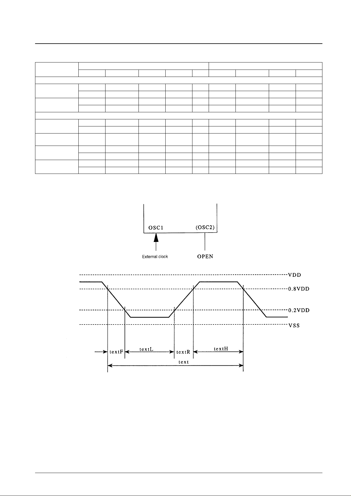
Table 1 Guaranteed Constants for Ceramic Oscillators
Figure 1 External Clock Input Waveform
No. 5117-12/39
LC6529N, LC6529F, LC6529L
Standard type Chip type
Oscillator type
Manufacturer Oscillator C1 C2 Rd Manufacturer Oscillator C1 C2
[External capacitor]
4-MHz ceramic
Murata CS A4.00MG 33 pF ±10% 33 pF ± 10% — Murata CS AC4.00MGC 33 pF ± 10% 33 pF ± 10%
oscillator
Kyocera KBR-4.0MSA 33 pF ± 10% 33 pF ± 10% — — — — —
2-MHz ceramic
Murata CS A2.00MG 33 pF ± 10% 33 pF ± 10% — Murata CS AC2.00MGC 33 pF ± 10% 33 pF ± 10%
oscillator
Kyocera KBR-2.0MSA 33 pF ± 10% 33 pF ± 10% — — — — —
[Built-in capacitor]
4-MHz ceramic
Murata CS A4.00MG — — — Kyocera KBR-4.0MWS — —
oscillator
Kyocera KBR-4.0MSA — — — — — — —
2-MHz ceramic
Murata CS A2.00MG — — — Kyocera KBR-2.0MWS — —
oscillator
800-kHz ceramic
Murata CS B800J
100 pF ± 10% 100 pF ± 10%
3.3 kΩ — — — —
oscillator
Kyocera KBR-800F/Y
150 pF ± 10% 150 pF ± 10%
— — — — —
400-kHz ceramic
Murata CS B400P
220 pF ± 10% 220 pF ± 10%
3.3 kΩ — — — —
oscillator
Kyocera KBR-400BK/Y
330 pF ± 10% 330 pF ± 10%
— — — — —
Page 13

Figure 2 2-Pin RC Oscillator Circuit Figure 3 Ceramic Oscillator Circuit
Figure 4 Oscillator Stabilization Interval
Figure 5 Comparator Response Speed (TRS) Timing
No. 5117-13/39
LC6529N, LC6529F, LC6529L
Page 14

Figure 6 Reset Circuit
LC6529N RC Oscillator Characteristics
Figure 7 gives the RC oscillator characteristics for the LC6529N. The frequency fluctuation ranges are as follows:
1. For VDD= 3.0 to 6.0 V, Ta = –40 to +85°C, Cext = 220 pF, and Rext = 12.0 kΩ,
309 kHz ≤ f
MOSC
≤ 577 kHz
2. For VDD= 4.0 to 6.0 V, Ta = –40 to +85°C, Cext = 220 pF, and Rext = 4.7 kΩ,
660 kHz ≤ f
MOSC
≤ 1229 kHz
These results are only guaranteed for the above RC constants.
If the above values are not available, keep the RC constants within the following ranges. (See Figure 7.)
Rext = 3 to 20 kΩ, Cext = 150 to 390 pF
Note: 1. The oscillator frequency must be within the range between 350 and 750 kHz for VDD= 5.0 V and Ta = 25°C.
2. Make sure that the oscillator frequency remains well within the operating clock frequency range (See
frequency divider option table.) for the two ranges VDD= 3.0 to 6.0 V, Ta = –40 to +85°C and VDD= 4.0 to
6.0 V, Ta = –40 to +85°C.
Figure 7 RC Oscillator Frequency Data (Sample Values)
No. 5117-14/39
LC6529N, LC6529F, LC6529L
Note: When the power supply rising interval is zero, a value of 0.1 µF
for CRES produces a reset interval of 10 to 100 ms. If the
power supply rising interval is larger, adjust CRES to produce a
minimum interval of 10 ms for the oscillation to stabilize.
Page 15

LC6529F
Absolute Maximum Ratings at Ta = 25°C, VSS= 0 V
Note: 1. When the oscillator circuit in Figure 3 and the guaranteed constant are used, this is guaranteed over the full amplitude.
2. Averaged over 100-ms interval.
Allowable Operating Ranges at Ta = –40 to +85°C, VSS= 0 V, VDD= 3.0 to 6.0 V
Note: * Maintain the power supply voltage at VDDuntil the HALT instruction has completed execution, placing the chip in the standby mode. Block
chattering from entering PA3 during the HALT instruction execution cycle.
No. 5117-15/39
LC6529N, LC6529F, LC6529L
Parameter Symbol Conditions min typ max Unit
Maximum supply voltage V
DD
max V
DD
–0.3 +7.0 V
V
I
1 OSC1
*1
–0.3 VDD+ 0.3
Input voltage V
I
2 TEST, RES –0.3 VDD+ 0.3 V
V
I
3 Port E (PE) configuration –0.3 VDD+ 0.3
Output voltage V
O
OSC2 Voltages up to that generated allowed. V
I/O voltages
V
IO
1 Open-drain (OD) configuration –0.3 +15
V
V
IO
2 Pull-up (PU) resistor configuration –0.3 VDD+ 0.3
Peak output current I
OP
PA, PC, PD –2 +20 mA
I
OA
PA, PC, PD: Average for pin over 100-ms interval –2 +20
Average output current
ΣI
OA
1 PA: Total current for pins PA0 to PA3
*2
–6 +40
mA
ΣI
OA
2
PC, PD: Total current for pins PC0 to PC3 and
–14 +90
PD0 to PD3
*2
Pd max1 Ta = –40 to +85°C (DIP24S) 360
Allowable power dissipation Pd max2 Ta = –40 to +85°C (SSOP24) 165 mW
Pd max3 Ta = –40 to +85°C (MFP30S) 150
Operating temperature Topr –40 +85
°C
Storage temperature Tstg –55 +125
Parameter Symbol Conditions min typ max Unit
Supply voltage V
DD
V
DD
3.0 6.0 V
Standby voltage V
ST
VDD: Preserves contents of RAM and registers*. 1.8 6.0 V
V
IH
1
Open-drain (OD) configuration: With output N-channel
0.7 V
DD
13.5
transistor off
VIH2
Pull-up (PU) resistor configuration: With output
0.7 V
DD
V
DD
Input high level voltage
N-channel transistor off
V
V
IH
3 PE: Using port E configuration 0.7 V
DD
V
DD
VIH4 RES: VDD= 1.8 to 6 V 0.8 V
DD
V
DD
VIH5 OSC1: Using external clock option 0.8 V
DD
V
DD
VIL1
PA, PC, PD: With output N-channel transistor off,
V
SS
0.3 V
DD
VDD= 4 to 6 V
V
IL
2 PA, PC, PD: With output N-channel transistor off V
SS
0.25 V
DD
VIL3 PE: Using port E configuration, VDD= 4 to 6 V V
SS
0.3 V
DD
VIL4 PE: Using port E configuration V
SS
0.25 V
DD
Input low level voltage
V
IL
5 OSC1: Using external clock option, VDD= 4 to 6 V V
SS
0.25 V
DD
V
VIL6 OSC1: Using external clock option V
SS
0.2 V
DD
VIL7 TEST: VDD= 4 to 6 V V
SS
0.3 V
DD
VIL8 TEST V
SS
0.25 V
DD
VIL9 RES: VDD= 4 to 6 V V
SS
0.25 V
DD
VIL10 RES V
SS
0.2 V
DD
Operating frequency fop 200 4330 kHz
(cycle time) (Tcyc) (20) (0.92) (µs)
[External clock conditions]
Frequency text 200 4330 kHz
Pulse width textH, textL OSC1: Figure 1 69
ns
Rise/fall times textR, textF 50
Oscillator guaranteed constants
Figure 2 See Table 1.
Ceramic oscillator
Page 16

Electrical Characteristics at Ta = –40 to +85°C, VSS= 0 V, VDD= 3.0 to 6.0 V
Note: * The RC oscillator and external clock options require a Schmidt trigger configuration for OSC1.
Note: * f
CFOSC
is the allowable oscillator frequency.
No. 5117-16/39
LC6529N, LC6529F, LC6529L
Parameter Symbol Conditions min typ max Unit
Open-drain (OD) configuration for port: With output
IIH1 N-channel transistor off. (Includes transistor’s leak 5.0
Input high level current
current.) V
IN
= 13.5 V
µA
I
IH
2 PE: Using port E configuration, VIN= V
DD
1.0
I
IH
3 OSC1: Using external clock option, VIN= V
DD
1.0
Open-drain (OD) configuration for port: With output
IIL1 N-channel transistor off. (Includes transistor’s leak –1.0
current.) V
IN
= V
SS
µA
Pull-up (PU) resistor configuration for port:
I
IL
2 With output N-channel transistor off. (Includes –220 –71.5
transistor’s leak current.) V
IN
= V
SS
Input low level current
Pull-up (PU) resistor configuration for port C:
I
IL
3 With output N-channel transistor off. (Includes –6.00 –2.17 mA
transistor’s leak current.) V
IN
= V
SS
IIL4 PE: Using port E configuration, VIN= V
SS
–1.0
I
IL
5 RES: VIN= V
SS
–45 –10 µA
I
IL
6 OSC1: Using external clock option, VIN= V
SS
–1.0
V
OH
1
Pull-up (PU) resistor configuration for port C:
VDD– 1.2
Output high level voltage
I
OH
= –300 µA, VDD= 4 to 6 V
V
V
OH
2
Pull-up (PU) resistor configuration for port C:
VDD– 0.5
I
OH
= –60 µA
V
OL
1 PA, PC, PD: IOL= 10 mA, VDD= 4 to 6 V 1.5
Output low level voltage
V
OL
2
PA, PC, PD: With I
OL
for each port less than or equal
0.4
V
to 1 mA, I
OL
= 1.8 mA
Hysteresis voltage
V
HIS
1 RES 0.1 V
DD
V
V
HIS
2 OSC1*: Using RC oscillator or external clock option 0.1 V
DD
Parameter Symbol Conditions min typ max Unit
[Current drain]
Ceramic oscillator I
DD OP
1
V
DD
: Figure 2, 4 MHz, 200 to 4330 kHz,
1.6 4.0
1/1 frequency divider
mA
External clock I
DD OP
2
Note: With output N-channel transistor off and
1.6 4.2
port level = V
DD
I
DD st
1
V
DD
: With output N-channel transistor off and
0.05 10
Standby operation
port level = V
DD
, VDD= 6 V
µA
I
DD st
2
V
DD
: With output N-channel transistor off and
0.025 5
port level = V
DD
, VDD= 3 V
[Oscillator characteristics] (Ceramic oscillator)
Oscillator frequency f
CFOSC
OSC1, OSC2: Figure 2, fO= 4 MHz* 3840 4000 4160 kHz
Oscillator stabilization interval t
CFS
Figure 3, fO= 4 MHz 10 ms
[Pull-up resistors]
Pull-up (PU) resistor configuration for port A or D:
RPP1 With output N-channel transistor off and V
IN
= VSS, 30 70 130
I/O ports
V
DD
= 5 V
Pull-up (PU) resistor configuration for port C:
kΩ
RPP2 With output N-channel transistor off and VIN= VSS, 1.0 2.3 3.9
V
DD
= 5 V
Reset port Ru RES: V
IN
= VSS, VDD= 5 V 200 500 725
External reset characteristic:
t
RST
See
Reset time Figure 5.
Pin capacitance C
P
f = 1 MHz, VIN= VSSfor pins other than one
10 pF
being measured
Page 17

Comparator Characteristics for Comparator Option at Ta = –40 to +85°C, VSS= 0 V, VDD= 3.0 to 6.0 V
Table 1. Guaranteed Constants for Ceramic Oscillators
Figure 1 External Clock Input Waveform
No. 5117-17/39
LC6529N, LC6529F, LC6529L
Parameter Symbol Conditions min typ max Unit
Reference input voltage range V
RFIN
V
REF
0, V
REF
1 VSS+ 0.3 VDD– 1.5 V
Inphase input voltage range V
CMIN
CMP0 to CMP3 V
SS
VDD– 1.5 V
Offset voltage V
OFF
V
CMIN
= VSSto VDD– 1.5 V ±50 ±300 mV
Response speed
TRS1 Figure 4: V
DD
= 4 to 6 V 1.0 5.0
µs
TRS2 Figure 4 1.0 200
Input high level current
I
IH
1 V
REF
0, V
REF
1 1.0
µA
I
IH
2 CMP0 to CMP3: Without feedback resistor option 1.0
Input low level current
I
IL
1 V
REF
0, V
REF
1 –1.0
µA
I
IL
2 CMP0 to CMP3: Without feedback resistor option –1.0
Feedback resistor RCMFB CMP0 to CMP3: With feedback resistor option 460 kΩ
Standard type Chip type
Oscillator type
Manufacturer Oscillator C1 C2 Rd Manufacturer Oscillator C1 C2
[External capacitor]
4-MHz ceramic
Murata CS A4.00MG 33 pF ± 10% 33 pF ± 10% — Murata CS AC4.00MGC 33 pF ± 10% 33 pF ± 10%
oscillator
Kyocera KBR-4.0MSA 33 pF ± 10% 33 pF ± 10% — — — — —
2-MHz ceramic
Murata CS A2.00MG 33 pF ± 10% 33 pF ± 10% — Murata CS AC2.00MGC 33 pF ± 10% 33 pF ± 10%
oscillator
Kyocera KBR-2.0MSA 33 pF ± 10% 33 pF ± 10% — — — — —
[Built-in capacitor]
4-MHz ceramic
Murata CS A4.00MG — — — Kyocera KBR-4.0MWS — —
oscillator
Kyocera KBR-4.0MSA — — — — — — —
2-MHz ceramic
Murata CS A2.00MG — — — Kyocera KBR-2.0MWS — —
oscillator
Page 18

Figure 2 Ceramic Oscillator Circuit Figure 3 Oscillator Stabilization Interval
Figure 4 Comparator Response Speed (TRS) Timing
No. 5117-18/39
LC6529N, LC6529F, LC6529L
Page 19

Figure 5 Reset Circuit
No. 5117-19/39
LC6529N, LC6529F, LC6529L
Note: When the power supply rising interval is zero, a value of 0.1 µF
for CRES produces a reset interval of 10 to 100 ms. If the
power supply rising interval is larger, adjust CRES to produce a
minimum interval of 10 ms for the oscillation to stabilize.
Page 20

LC6529L
Absolute Maximum Ratings at Ta = 25°C, VSS= 0 V
Note: 1. When the oscillator circuit in Figure 3 and the guaranteed constant are used, this is guaranteed over the full amplitude.
2. Averaged over 100-ms interval.
Allowable Operating Ranges at Ta = –40 to +85°C, VSS= 0 V, VDD= 2.2 to 6.0 V
Note: * Maintain the power supply voltage at VDDuntil the HALT instruction has completed execution, placing the chip in the standby mode. Block
chattering from entering PA3 during the HALT instruction execution cycle.
No. 5117-20/39
LC6529N, LC6529F, LC6529L
Parameter Symbol Conditions min typ max Unit
Maximum supply voltage V
DD
max V
DD
–0.3 +7.0 V
V
I
1 OSC1
*1
–0.3 VDD+ 0.3
Input voltage V
I
2 TEST, RES –0.3 VDD+ 0.3 V
V
I
3 Port E (PE) configuration –0.3 VDD+ 0.3
Output voltage V
O
OSC2 Voltages up to that generated allowed. V
I/O voltages
V
IO
1 Open-drain (OD) configuration –0.3 +15
V
V
IO
2 Pull-up (PU) resistor configuration –0.3 VDD+ 0.3
Peak output current I
OP
PA, PC, PD –2 +20 mA
I
OA
PA, PC, PD: Average for pin over 100-ms interval –2 +20
Average output current
ΣI
OA
1 PA: Total current for pins PA0 to 3
*2
–6 +40
mA
ΣI
OA
2
PC, PD: Total current for pins PC0 to PC3 and
–14 +90
PD0 to PD3
*2
Pd max1 Ta = –40 to +85°C (DIP24S) 360
Allowable power dissipation Pd max2 Ta = –40 to +85°C (SSOP24) 165 mW
Pd max3 Ta = –40 to +85°C (MFP30S) 150
Operating temperature Topr –40 +85
°C
Storage temperature Tstg –55 +125
Parameter Symbol Conditions min typ max Unit
Supply voltage V
DD
V
DD
2.2 6.0 V
Standby voltage V
ST
VDD: Preserves contents of RAM and registers*. 1.8 6.0 V
V
IH
1
Open-drain (OD) configuration: With output N-channel
0.7 V
DD
13.5
transistor off
VIH2
Pull-up (PU) resistor configuration: With output
0.7 V
DD
V
DD
Input high level voltage
N-channel transistor off
V
V
IH
3 PE: Using port E configuration 0.7 V
DD
V
DD
VIH4 RES: VDD= 1.8 to 6 V 0.8 V
DD
V
DD
VIH5 OSC1: Using external clock option 0.8 V
DD
V
DD
VIL1 PA, PC, PD: With output N-channel transistor off V
SS
0.2 V
DD
VIL2 PE: Using port E configuration V
SS
0.2 V
DD
Input low level voltage VIL3 OSC1: Using external clock option V
SS
0.15 V
DD
V
V
IL
4 TEST V
SS
0.2 V
DD
VIL5 RES V
SS
0.15 V
DD
Operating frequency fop Using the built-in 1/3 or 1/4 frequency dividers extends 200 1040 kHz
(cycle time) (Tcyc) the maximum to 4.16 MHz. (20) (3.84) (µs)
[External clock conditions]
Frequency text 200 4160 kHz
Pulse width textH, textL 120
ns
Rise/fall times textR, textF 100
[Oscillator guaranteed constants]
2-pin RC oscillator circuit
Cext OSC1, OSC2: Figure 2 220 ± 5% pF
Rext OSC1, OSC2: Figure 2 12.0 ± 1% kΩ
Ceramic oscillator Figure 3 See Table 1.
OSC1: If the clock frequency exceeds 1.040 MHz,
use the built-in 1/3 or 1/4 frequency divider. Figure 1
Page 21

Electrical Characteristics at Ta = –40 to +85°C, VSS= 0 V, VDD= 2.2 to 6.0 V
Note: * The RC oscillator and external clock options require a Schmidt trigger configuration for OSC1.
No. 5117-21/39
LC6529N, LC6529F, LC6529L
Parameter Symbol Conditions min typ max Unit
Open-drain (OD) configuration for port: With output
IIH1 N-channel transistor off. (Includes transistor’s leak 5.0
Input high level current
current.) V
IN
= 13.5 V
µA
I
IH
2 PE: Using port E configuration, VIN= V
DD
1.0
I
IH
3 OSC1: Using external clock option, VIN= V
DD
1.0
Open-drain (OD) configuration for port: With output
IIL1 N-channel transistor off. (Includes transistor’s leak –1.0
current.) V
IN
= V
SS
µA
Pull-up (PU) resistor configuration for port:
I
IL
2 With output N-channel transistor off. (Includes –220 –71.5
transistor’s leak current.) V
IN
= V
SS
Input low level current
Pull-up (PU) resistor configuration for port C:
I
IL
3 With output N-channel transistor off. (Includes –6.00 –2.17 mA
transistor’s leak current.) V
IN
= V
SS
IIL4 PE: Using port E configuration, VIN= V
SS
–1.0
I
IL
5 RES: VIN= V
SS
–45 –10 µA
I
IL
6 OSC1: Using external clock option, VIN= V
SS
–1.0
Output high level voltage V
OH
Pull-up (PU) resistor configuration for port C:
V
DD
– 0.5 V
I
OH
= –50 µA
V
OL
1 PA, PC, PD: IOL= 3 mA 1.5
Output low level voltage
V
OL
2
PA, PC, PD: With I
OL
for each port less than
0.4
V
or equal to 1 mA, I
OL
= 1 mA
Hysteresis voltage
V
HIS
1 RES 0.1 V
DD
V
V
HIS
2 OSC1*: Using RC oscillator or external clock option 0.1 V
DD
Parameter Symbol Conditions min typ max Unit
[Current drain]
RC oscillator I
DD OP
1 VDD: Figure 2, 400 kHz (typ) 0.4 1.0
I
DD OP
2 VDD: Figure 3, 4 MHz, 1/4 frequency divider 1.6 4.0
I
DD OP
3
V
DD
: Figure 3, 4 MHz, 1/4 frequency divider,
0.4 0.8
V
DD
= 2.2 V
I
DD OP
4 VDD: Figure 3, 2 MHz, 1/3 frequency divider 1.3 3.0
mA
Ceramic oscillator I
DD OP
5 VDD: Figure 3, 2 MHz, 1/4 frequency divider 1.3 3.0
I
DD OP
6
V
DD
: Figure 3, 2 MHz, 1/3, 1/4 frequency divider
0.3 0.6
V
DD
= 2.2 V
I
DD OP
7 VDD: Figure 3, 800 kHz 1.1 2.6
I
DD OP
8 VDD: Figure 3, 400 kHz 0.9 2.4
V
DD
: 200 to 667 kHz, 1/1 frequency divider,
External clock I
DD OP
9 600 to 2000 kHz, 1/3 frequency divider, 1.0 2.5 mA
800 to 2667 kHz, 1/4 frequency divider
I
DD
st1
V
DD
: With output N-channel transistor off and
0.05 10
Standby operation
port level = V
DD
, VDD= 6 V
µA
I
DD
st2
V
DD
: With output N-channel transistor off and
0.025 5
port level = V
DD
, VDD= 2.2 V
[Oscillator characteristics]
RC oscillator Oscillator frequency f
MOSC
OSC1, OSC2: Figure 2, Cext = 220 pF ± 5%,
275 400 577 kHz
Rext = 12.0 kΩ ± 1%
[Oscillator characteristics] (Ceramic oscillator)
OSC1, OSC2: Figure 3, f
O
= 400 kHz 384 400 416
OSC1, OSC2: Figure 3, f
O
= 800 kHz 768 800 832
Oscillator frequency f
CFOSC
*
OSC1, OSC2: Figure 3, f
O
= 2 MHz 1920 2000 2080
kHz
OSC1, OSC2: Figure 3, f
O
= 4 MHz,
3840 4000 4160
1/4 frequency divider
Figure 4, f
O
= 400 kHz 10
Oscillator stabilization interval t
CFS
Figure 4, fO= 800 kHz,
10
ms
f
O
= 2 MHz, 1/3, 1/4 frequency divider,
f
O
= 4 MHz, 1/4 frequency divider
Continued on next page.
Page 22

Continued from preceding page.
Note * f
CFOSC
is the allowable oscillator frequency.
Comparator Characteristics for Comparator Option at Ta = –40 to +85°C, VSS= 0 V, VDD= 3.0 to 6.0 V
Table 1 Guaranteed Constants for Ceramic Oscillators
No. 5117-22/39
LC6529N, LC6529F, LC6529L
Parameter Symbol Conditions min typ max Unit
Reference input voltage range V
RFIN
V
REF
0, V
REF
1 VSS+ 0.3 VDD– 1.5 V
Inphase input voltage range V
CMIN
CMP0 to CMP3 V
SS
VDD– 1.5 V
Offset voltage V
OFF
V
CMIN
= VSSto VDD– 1.5 V ±50 ±300 mV
Response speed TRS Figure 5 1.0 200 µs
Input high level current
I
IH
1 V
REF
0, V
REF
1 1.0
µA
I
IH
2 CMP0 to CMP3: Without feedback resistor option 1.0
Input low level current
I
IL
1 V
REF
0, V
REF
1 –1.0
µA
I
IL
2 CMP0 to CMP3: Without feedback resistor option –1.0
Feedback resistor RCMFB CMP0 to CMP3: With feedback resistor option 460 kΩ
Parameter Symbol Conditions min typ max Unit
[Pull-up resistors]
Pull-up (PU) resistor configuration for port A or D:
RPP1 With output N-channel transistor off and V
IN
= VSS, 30 70 130
I/O ports
V
DD
= 5 V
Pull-up (PU) resistor configuration for port C:
kΩ
RPP2 With output N-channel transistor off and VIN= VSS, 1.0 2.3 3.9
V
DD
= 5 V
Reset port Ru RES: V
IN
= VSS, VDD= 5 V 200 500 725
External reset characteristic:
t
RST
See
Reset time Figure 6.
Pin capacitance C
P
f = 1 MHz, VIN= VSSfor pins other than one
10 pF
being measured
Standard type Chip type
Oscillator type
Manufacturer Oscillator C1 C2 Rd Manufacturer Oscillator C1 C2
[External capacitor]
4-MHz ceramic
Murata CS A4.00MG 33 pF ± 10% 33 pF ± 10% — Murata CS AC4.00MGC 33 pF ± 10% 33 pF ± 10%
oscillator
Kyocera KBR-4.0MSA 33 pF ± 10% 33 pF ± 10% — — — — —
2-MHz ceramic
Murata CS A2.00MG 33 pF ± 10% 33 pF ± 10% — Murata CS AC2.00MGC 33 pF ± 10% 33 pF ± 10%
oscillator
Kyocera KBR-2.0MSA 33 pF ± 10% 33 pF ± 10% — — — — —
[Built-in capacitor]
4-MHz ceramic
Murata CS A4.00MG — — — Kyocera KBR-4.0MWS — —
oscillator
Kyocera KBR-4.0MSA — — — — — — —
2-MHz ceramic
Murata CS A2.00MG — — — Kyocera KBR-2.0MWS — —
oscillator
800-kHz ceramic
Murata CS B800J
100 pF ± 10% 100 pF ± 10%
3.3 kΩ — — — —
oscillator
Kyocera KBR-800F/Y
150 pF ± 10% 150 pF ± 10%
— — — — —
400-kHz ceramic
Murata CS B400P
220 pF ± 10% 220 pF ± 10%
3.3 kΩ — — — —
oscillator
Kyocera KBR-400BK/Y
330 pF ± 10% 330 pF ± 10%
— — — — —
Page 23

Figure 1 External Clock Input Waveform
Figure 2 2-Pin RC Oscillator Circuit Figure 3 Ceramic Oscillator Circuit
No. 5117-23/39
LC6529N, LC6529F, LC6529L
Page 24

Figure 4 Oscillator Stabilization Interval
Figure 5 Comparator Response Speed (TRS) Timing
Figure 6 Reset Circuit
No. 5117-24/39
LC6529N, LC6529F, LC6529L
Note: When the power supply rising interval is zero, a value of 0.1 µF
for CRES produces a reset interval of 10 to 100 ms. If the
power supply rising interval is larger, adjust CRES to produce a
minimum interval of 10 ms for the oscillation to stabilize.
Page 25

LC6529L RC Oscillator Characteristics
Figure 7 gives the RC oscillator characteristics for the LC6529L. The frequency fluctuation range is as follows:
For VDD= 2.2 to 6.0 V, Ta = –40 to +85°C, Cext = 220 pF, and Rext = 12.0 kΩ,
275 kHz ≤ = f
MOSC
≤ = 577 kHz
These results are only guaranteed for the above RC constants.
If the above values are not available, keep the RC constants within the following ranges: (See Figure 7.)
Rext = 3 to 20 kΩ, Cext = 150 to 390 pF
Note: 1. The oscillator frequency must be within the range between 350 and 750 kHz for VDD= 5.0 V and Ta = 25°C.
2. Make sure that the oscillator frequency remains well within the operating clock frequency range (See
frequency divider option table.) for the range VDD= 2.2 to 6.0 V, Ta = –40 to +85°C.
Figure 7 RC Oscillator Frequency Data (Sample Values)
No. 5117-25/39
LC6529N, LC6529F, LC6529L
Page 26

LC6529N/F/L Instruction Table (by Function)
Abbreviations:
Note: * The second and subsequent repetitions of an LI or CLA instruction produce the same effects as an NOP instruction.
AC: Accumulator
ACt: Accumulator bit t
CF: Carry flag
DP: Data pointer
E: E register
M: Memory
M (DP): Memory addressed by DP
P (DPL): I/O port specified by DP
L
PC: Program counter
STACK Stack register
TM: Timer
TMF: Timer overflow flag
ZF: Zero flag
( ), [ ]: Indicates the contents of a location
←: Transfer direction, result
+: Addition
–: Subtraction
: Exclusive or
No. 5117-26/39
LC6529N, LC6529F, LC6529L
Continued on next page.
Instruction code Affected
Mnemonic Operation Description status Note
D
7D6D5D4D3D2D1D0
bits
[Accumulator manipulation instructions]
CLA Clear AC 1 1 0 0 0 0 0 0 1 1 AC ← 0 Set AC to zero. ZF *
CLC Clear CF 1 1 1 0 0 0 0 1 1 1 CF ← 0 Clear CF to zero. CF
STC Set CF 1 1 1 1 0 0 0 1 1 1 CF ← 1 Set CF to one. CF
CMA Complement AC 1 1 1 0 1 0 1 1 1 1 AC ← (AC) Take ones complement of AC. ZF
INC Increment AC 0 0 0 0 1 1 1 0 1 1 AC ← (AC) + 1 Add one to AC. ZF, CF
DEC Decrement AC 0 0 0 0 1 1 1 1 1 1 AC ← (AC) – 1 Subtract one from AC. ZF, CF
TAE Transfer AC to E 0 0 0 0 0 0 1 1 1 1 E ← (AC) Copy contents of AC to E.
XAE Exchange AC with E 0 0 0 0 1 1 0 1 1 1 (AC) ↔ (E)
Exchange contents of
AC and E.
[Memory manipulation instructions]
INM Increment M 0 0 1 0 1 1 1 0 1 1
M (DP) ←
Add one to M (DP). ZF, CF
[M (DP)] + 1
DEM Decrement M 0 0 1 0 1 1 1 1 1 1
M (DP) ←
Subtract one from M (DP). ZF, CF
[M (DP)] – 1
SMB bit Set M data bit 0 0 0 0 1 0 B
1B0
1 1 M (DP, B1B0) ← 1
Set bit specified by immediate
data B
1B0
in M (DP) to one.
Clear bit specified by
RMB bit Reset M data bit 0 0 1 0 1 0 B1B01 1 M (DP, B1B0) ← 0 immediate data B1B0in ZF
M (DP) to zero.
[Arithmetic, logic and comparison instructions]
AC ← (AC) +
Add contents of M (DP) to
AD Add M to AC 0 1 1 0 0 0 0 0 1 1
[M (DP)]
contents of AC and store ZF, CF
result in AC.
AC ← (AC) +
Add contents of M (DP) and
ADC Add M to AC with CF 0 0 1 0 0 0 0 0 1 1
[M (DP)] + (CF)
CF to contents of AC and ZF, CF
store result in AC.
DAA
Decimal adjust AC
1 1 1 0 0 1 1 0 1 1 AC ← (AC) + 6 Add 6 to contents of AC. ZF
in addition
DAS
Decimal adjust AC
1 1 1 0 1 0 1 0 1 1 AC ← (AC) + 10 Add 10 to contents of AC. ZF
in subtraction
AC ← (AC)
XOR contents of AC with
EXL Exclusive or M to AC 1 1 1 1 0 1 0 1 1 1
[M (DP)]
contents of M (DP) and store ZF
result in AC.
Compare contents of M (DP)
with those of AC and set CF
and ZF according to result.
CM Compare AC with M 1 1 1 1 1 0 1 1 1 1 [M (DP)] + (AC) + 1 ZF, CF
Number of
bytes
Number of
cycles
Page 27

Continued from preceding page.
Note: * The second and subsequent repetitions of an LI or CLA instruction produce the same effects as an NOP instruction.
No. 5117-27/39
LC6529N, LC6529F, LC6529L
Instruction code Affected
Mnemonic Operation Description status Note
D
7D6D5D4D3D2D1D0
bits
[Accumulator manipulation instructions]
Compare contents of
immediate data field
(I
3I2I1I0
) with those of AC
and set CF and ZF according
Compare AC with 0 0 1 0 1 1 0 0
to result.
CI data
immediate data 0 1 0 0 I
3I2I1I0
2 2 I3I2I1I0+ (AC) + 1 ZF, CF
[Load and store instructions]
Load AC with
Load AC with contents of
LI data
immediate data
1 1 0 0 I
3I2I1I0
1 1 AC ← I3I2I1I
0
immediate data field ZF *
(I
3I2I1I0
).
S Store AC to M 0 0 0 0 0 0 1 0 1 1 M (DP) ← (AC)
Copy contents of AC to
M (DP).
L Load AC from M 0 0 1 0 0 0 0 1 1 1 AC ← [M (DP)] Copy contents of M (D) to AC. ZF
[Data pointer manipulation instructions]
Load DP
H
with zero
Clear DP
H
to zero and copy
LDZ and DP
L
with
1 0 0 0 I
3I2I1I0
1 1
DP
H
← 0
contents of immediate data
data immediate data DP
L
← I3I2I1I
0
field (I3I2I1I0) to DPL.
respectively
LHI data
Load DP
H
with
0 1 0 0 0 0 I
1I0
1 1 DPH← I1I
0
Copy contents of immediate
immediate data data field (I
1I0
) to DPH.
IND Increment DP
L
1 1 1 0 1 1 1 0 1 1 DPL← (DPL) + 1 Add one to DPL. ZF
DED Decrement DP
L
1 1 1 0 1 1 1 1 1 1 DPL← (DPL) – 1 Subtract one from DPL. ZF
TAL Transfer AC to DP
L
1 1 1 1 0 1 1 1 1 1 DPL← (AC) Copy contents of AC to DPL.
TLA Transfer DP
L
to AC 1 1 1 0 1 0 0 1 1 1 AC ← (DPL) Copy contents of DPLto AC. ZF
[Jump and subroutine instructions]
JMP 0 1 1 0 1 0 P
9P8
PC ← P9P8P7P6Jump to address in immediate
addr
Jump
P7P6P5P4P3P2P1P
0
2 2 P5P4P3P2data field (P9P8P7P6P5P
4
P1P
0
P3P2P1P0).
STACK ← (PC) + 1
CZP Call subroutine in
PC9to PC6, PC1,
addr the zero page
1 0 1 1 P
3P2P1P0
1 1 PC0← 0 Call subroutine in zero page.
PC
5
to PC2←
P
3P2P1P0
STACK ← (PC) + 2
CAL
Call subroutine
1 0 1 0 1 0 P
9P8
2 2
P
9
to P0← 0
Call subroutine.
addr P
7P6P5P4P3P2P1P0
P9P8P7P6P5P
4
P3P2P1P
0
RT
Return from
0 1 1 0 0 0 1 0 1 1 PC ← (STACK) Return from subroutine.
subroutine
[Branch instructions]
PC
7
to PC0← Branch to specified address
The mnemonic
BAt 0 1 1 1 0 1 t
1t0
P7P6P5P
4
in same page (P7to P0) if bit
includes decimal
addr
Branch on AC bit
P
7P6P5P4P3P2P1P0
2 2
P
3P2P1P0
specified by immediate data
equivalent t of
if ACt = 1 t
1t0
in AC is one.
immediate data
i.e., BA0 to BA3.
The mnemonic
PC
7
to PC0← Branch to specified address includes decimal
BNAt
Branch on no AC bit
0 0 1 1 0 0 t
1t0
2 2
P
7P6P5P4
in same page (P7to P0) if bit equivalent t of
addr P
7P6P5P4P3P2P1P0
P3P2P1P
0
specified by immediate data immediate data
if ACt = 0 t
1t0
in AC is zero. i.e., BNA0 to
BNA3.
PC7to PC0←
Branch to specified address
The mnemonic
BMt 0 1 1 1 0 1 t1t
0
P7P6P5P
4
in same page (P7to P0) if bit
includes decimal
addr
Branch on M bit
P
7P6P5P4P3P2P1P0
2 2 P3P2P1P
0
specified by immediate data
equivalent t of
if [M (DP, t
1t0
)]
t
1t0
in M (DP) is one.
immediate data
= 1 i.e., BM0 to BM3.
Number of
bytes
Number of
cycles
Magnitude
CF ZF
comparison
I
3I2I1I0
> AC 0 0
I
3I2I1I0
= AC 1 1
I
3I2I1I0
< AC 1 0
Continued on next page.
Page 28

Continued from preceding page.
No. 5117-28/39
LC6529N, LC6529F, LC6529L
Instruction code Affected
Mnemonic Operation Description status Note
D
7D6D5D4D3D2D1D0
bits
[Branch instructions]
PC
7
to PC0←
The mnemonic
P
7P6P5P4
Branch to specified address includes decimal
BNMt
Branch on no M bit
0 0 1 1 0 1 t
1t0
2 2 P3P2P1P
0
in same page (P7to P0) if bit equivalent t of
addr P
7P6P5P4P3P2P1P0
if [M (DP, t1t0)]
specified by immediate data immediate data
= 0
t
1t0
in M (DP) is zero. i.e., BNM0 to
BNM3.
PC7to PC0←
Branch to specified address
The mnemonic
BPt 0 1 1 1 1 0 t1t
0
P7P6P5P
4
in same page (P7to P0) if bit
includes decimal
addr
Branch on port bit
P
7P6P5P4P3P2P1P0
2 2 P3P2P1P
0
specified by immediate data
equivalent t of
if [P (DP
L
, t1t0)]
t
1t0
in P (DPL) is one.
immediate data
= 1 i.e., BP0 to BP3.
PC
7
to PC0←
The mnemonic
P
7P6P5P4
Branch to specified address includes decimal
BNPt
Branch on no port bit
0 0 1 1 1 0 t
1t0
2 2 P3P2P1P
0
in same page (P7to P0) if bit equivalent t of
addr P
7P6P5P4P3P2P1P0
if [P (DPL, t1t0)]
specified by immediate data immediate data
= 0
t
1t0
in P (DPL) is zero. i.e., BNP0 to
BNP3.
PC7to PC0←
Branch to specified address
BTM 0 1 1 1 1 1 0 0
P
7P6P5P4
in same page (P7to P0)
addr
Branch on timer
P
7P6P5P4P3P2P1P0
2 2 P3P2P1P
0
if TMF is one. Clear TMF
TMF
if TMF = 1
to zero.
then TMF ← 0
PC
7
to PC0←
Branch to specified address
BNTM 0 0 1 1 1 1 0 0
P
7P6P5P4
in same page (P7to P0)
addr
Branch on no timer
P
7P6P5P4P3P2P1P0
2 2 P3P2P1P
0
if TMF is zero. Clear TMF
TMF
if TMF = 0
to zero.
then TMF ← 0
PC
7
to PC0←
Branch to specified address
BC
Branch on CF
0 1 1 1 1 1 1 1
2 2
P
7P6P5P4
in same page (P7to P0)
addr P
7P6P5P4P3P2P1P0
P3P2P1P
0
if CF is one.
if CF = 1
PC
7
to PC0←
Branch to specified address
BNC
Branch on no CF
0 0 1 1 1 1 1 1
2 2
P
7P6P5P4
in same page (P7to P0)
addr P
7P6P5P4P3P2P1P0
P3P2P1P
0
if CF is zero.
if CF = 0
PC
7
to PC0←
Branch to specified address
BZ
Branch on ZF
0 1 1 1 1 1 1 0
2 2
P
7P6P5P4
in same page (P7to P0)
addr P
7P6P5P4P3P2P1P0
P3P2P1P
0
if ZF is one.
if ZF = 1
PC
7
to PC0←
Branch to specified address
BNZ
Branch on no ZF
0 0 1 1 1 1 1 0
2 2
P
7P6P5P4
in same page (P7to P0)
addr P
7P6P5P4P3P2P1P0
P3P2P1P
0
if ZF is zero.
if ZF = 0
[I/O instructions]
IP Input port to AC 0 0 0 0 1 1 0 0 1 1 AC ← [P (DP
L
)]
Copy contents of port
ZF
specified by P (PD
L
) to AC.
OP Output AC to port 0 1 1 0 0 0 0 1 1 1 P (DP
L
) ← (AC)
Copy contents of AC to port
specified by P (DP
L
).
Set bit specified by immediate
Execution of this
SPB bit Set port bit 0 0 0 0 0 1 B
1B0
1 2 P (DPL, B1B0) ← 1 data B1B0in port specified
instruction
by P (DP
L
) to one.
invalidates
contents of E.
Clear bit specified by
Execution of this
RPB bit Reset port bit 0 0 1 0 0 1 B
1B0
1 2 P (DPL, B1B0) ← 0 immediate data B1B0in port ZF
instruction
specified by P (DP
L
) to zero.
invalidates
contents of E.
[Other instructions]
WTTM Write timer 1 1 1 1 1 0 0 1 1 1
TM ← (E), (AC) Copy contents of E and AC to
TMF
TMF ← 0 timer. Clear TMF to zero.
Execution
HALT Halt 1 1 1 1 0 1 1 0 1 1 Halt Suspend all operations. requires that pin
PA3 be high.
NOP No operation 0 0 0 0 0 0 0 0 1 1 No operation
Do nothing but consume one
machine cycle.
Number of
bytes
Number of
cycles
Page 29

The above subset excludes the following instructions from the LC6523, 6526 set
AND, BFn, BI, BNFn, BNI, CLI, JPEA, OR, RAL, RCTL, RFB, TRI, RTBL, SCTL, SFB, X, XAH, XA0, XA1, XA3,
XD, XH0, XH1, XI, XL0, XL1, and XM.
Specifying LC6529N/F/L User Options
Specifying (Ordering) LC6529N/F/L User Options
When developing the software or ordering the chip, the user must prepare an EPROM containing the user program, user
option data, and fixed data. There are two ways of preparing these last two: with software provided by Sanyo and
manually. This Section discusses both methods.
Using Sanyo’s Option Specification Software
SU60K, the software for specifying LC6529 options, interactively asks the user to specify the options and writes the
results to a mask option file, file.OPT.
The M60K macro assembler assembles the user program into an object file, file.OBJ.
The L60K linker merges the mask option and object files to create an EVA file, file.EVA.
The EVA2HEX conversion tool converts the user program and mask options inside the EVA file to an object file in
hexadecimal (HEX) format.
The user use a PROM writer to download this HEX file to the EPROM submitted when ordering the chip.
For further details, see Figure A below and refer to the LC65/66K Software Manual.
Alternate Method
1. Overview
If not using the software for specifying LC6529 options, the user must list the mask options using the coding
procedures described below and then write these with the program to the EPROM regions shown in Figure A.
When ordering, the user must submit an option table list as well as the EPROM. Figure B gives an example of such a
list.
The procedures for coding the mask options appear on the pages following Figure B.
Figure A LC6529 ROM Data
No. 5117-29/39
LC6529N, LC6529F, LC6529L
Page 30

2. Sample option table list
Figure B Sample Option Table List
No. 5117-30/39
LC6529N, LC6529F, LC6529L
Page 31

Coding LC6529N/L Mask Options
No. 5117-31/39
LC6529N, LC6529F, LC6529L
Page 32

Coding LC6529F Mask Options
No. 5117-32/39
LC6529N, LC6529F, LC6529L
Page 33

Using Standby HALT Mode
The LC6529N/F/L features a convenient HALT mode that reduces current drain while the chip is on standby.
These standby functions involve the use of one instruction (HALT) and two control signal pins (PA3 and RES). For the
functions to work properly, the design of external circuits and chip software must pay due attention to these three.
Depending on how extensively the standby functions are used, the designer must consider and provide countermeasures
that protect the design from the effects of power supply fluctuations, power interruptions, external noise, and other
adverse conditions.
This document discusses the circuit and program design issues related to the most frequent application of the standby
functions, the detection and recovery from power outages.
When using the standby functions, follow the sample circuits given in this document and carefully observe all warnings
accompanying them.
Departures from the design guidelines herein will warrant thorough testing and evaluation of the effects of such sudden
changes in the operating environment as momentary power outages on application operation.
1. Entering and leaving the HALT mode
Table 1 gives the conditions for entering and leaving the HALT mode.
Table 1 Entering and Leaving the HALT Mode
Note: The second method for leaving the HALT mode is only available when the design uses an RC oscillator circuit. It may not work properly with a ceramic
oscillator circuit.
2. Important notes
Using the standby functions requires close attention to the following issues in application circuit and software design.
• The power supply voltage must not fall below the rating while the chip is on standby.
• Carefully observe all timing restrictions for the control signals during transitions to and from the HALT mode.
• Make sure that a signal for leaving the HALT mode does not overlap the execution of the HALT instruction.
This document demonstrates how to observe these restrictions by discussing both application circuits for a power
failure recovery function and programming considerations.
Such a power failure recovery function detects failure of the main power supply and causes the chip to execute a
HALT instruction to put itself on standby. Reducing the current drain this way allows the backup capacitor to
maintain the register contents for a longer period than otherwise possible. When the power is restored, the chip is
reset and automatically resumes execution with the program counter set to 000H. The following examples discuss
how the software can then distinguish this type of reset from a power on reset sequence along with issues related to
dealing with momentary AC power outages.
• Example 1
The first example does not distinguish a power-on reset sequence from a reset trigger by a power failure.
— Circuit diagram
Figure 2-1 gives the circuit diagram for this sample circuit.
No. 5117-33/39
LC6529N, LC6529F, LC6529L
Entering HALT mode Leaving HALT mode
HALT instruction while PA3 is high.
1. Reset signal (RES pin pulled low.)
2. PA3 pulled low.
Page 34

Note: All ports other than PA3 are configured as normal input ports.
Figure 2-1 Power Outage Backup Example 1
— Waveforms during operation
Figure 2-2 gives the waveforms relevant to the operation of the above circuit. There are three main states: (a)
power-on reset sequence, (b) momentary break in main power supply, and (c) recovery from power outage
backup state.
Note: V
+
TRON
= V+level at which transistor switches on and off
Figure 2-2 Waveforms Relevant to Operation of Circuit Example 1
No. 5117-34/39
LC6529N, LC6529F, LC6529L
Unit (resistance: Ω)
Page 35

— Main circuit states
a: Power-on reset sequence
Once the power supply voltage has reached the proper level, the chip automatically resets and begins
execution with the program counter set to 000H.
Caution: This circuit does not reset the chip until the power supply voltage is within the range specified for
VDD, so leaves the chip in an indeterminate state.
b: Momentary break in main power supply
i. If only the RES pin and none of the Pxx pins drops below the threshold level VIL, the chip resets and
repeats the power-on reset sequence.
ii. If the RES pin and the Pxx pins remain above the threshold level VIL, the chip continues normal
execution.
iii. If both the RES pin and the Pxx pins drop below the threshold level VIL, the chip resets if two
consecutive polls fail to detect a low at Pxx or, if a low is found, enters the HALT mode and then,
because the power has been restored, leaves the HALT mode.
c: Recovery from power outage backup state
Since the power has been restored, the chip leaves the HALT mode.
— Design considerations
a: V+rise time and C2
The V+rise time must be approximately ten times the RC constant for the reset circuit, C2 × R, where R is
the internal resistance (typ. 200 kΩ). It must also be no longer than approximately 20 ms.
b: R1 and C1 values
R1 must be as small as possible; C1, as large as possible to provide the longest backup time. At the same
time, however, R1 must be large enough such that the C1 charging current does not exceed the power
supply capacity.
c: R2 and R3 values
Choose these to make the Pxx high levels equal to VDD.
d: R4 value
Select R4 and thus the RC constant for C2 and R4 so that C2 discharges sometime in the interval between
the point at which V+falls below V
+
TRON
(turning off the transistor) and the point at which Pxx falls below
VIL. (Otherwise, the chip will enter the HALT mode and then not respond to a reset.)
e: R5 and R6 values
Select R5 and R6 so that V+when the reset circuit operates, switching on the transistor (that is, when R5
and R6 produce a VBEof approximately 0.6 V) is at least the minimum operating voltage (VDD) plus the
VFfor diode D1. To provide a rapid reset once the power is restored, however, keep this voltage as small as
possible while still satisfying these conditions.
f: Calculating backup time
From the time that the chip detects the power outage at Pxx until it executes the HALT instruction, the chip
operates normally so drains relatively large amounts of current. C1 must therefore be large enough to
provide backup power not only for the set's backup period, but for this transitional period as well.
— Software considerations
a: Assign signals so that PA3 is maintained high during standby operation.
b: The software should double-check a standby request by polling twice.
Example:
BP1 AAA : Poll once
BP1 AAA : Poll twice
HALT : Begin standby operation
AAA :
No. 5117-35/39
LC6529N, LC6529F, LC6529L
Page 36

• Example 2
The second example distinguishes a power-on reset sequence from a reset trigger by a power failure.
— Circuit diagram
Figure 2-3 gives the circuit diagram for this sample circuit.
Note: All ports other than PA3 are configured as normal input ports.
Figure 2-3 Power Outage Backup Example 2
— Waveforms during operation
Figure 2-4 gives the waveforms relevant to the operation of the above circuit. There are two main states: (a)
power-on reset sequence and (b) recovery from power outage backup state.
Note: V
+
TRON
= V+level at which transistor switches on and off
Figure 2-4 Waveforms Relevant to Operation of Circuit Example 2
No. 5117-36/39
LC6529N, LC6529F, LC6529L
Page 37

— Main circuit states
a: Power-on reset sequence
The operation and points to watch are the same as for the first example. The only difference is that the
software interprets a low at Pxx as indicating an initial reset.
b: Switch to standby operation
The chip polls Pxx and, if it is low, enters the HALT mode.
c: Recovery from power outage backup state
Since the power has been restored, the chip leaves the HALT mode. If the recovery routine then finds that
Pxx is high, it switches to a separate routine for restarting after a power outage.
Caution: If the power supply voltage VDDdrops below the VIHlevel for Pxx during the outage, this
recovery routine will subsequently find that Pxx is low and execute the routine for an initial reset instead.
— Design considerations
a: R2 and R3 values
Make R2 much greater than R1 and choose R3 to limit TR2’s IB.
b: R4 value
Since there are no momentary outages, the value is not critical, but select R4 so that C2 quickly discharges.
In all other respects, the same considerations apply as in Example 1.
— Software considerations
a: Assign signals so that PA3 is maintained high during standby operation.
b: The software should check for a standby request by polling once.
Example:
• Example 3
The third example adds support for momentary power outages.
— Circuit diagram
Figure 2-5 gives the circuit diagram for this sample circuit.
Note: All ports other than PA3 are configured as normal input ports.
Figure 2-5 Power Outage Backup Example 3
BP1 AAA : Poll port
HALT : Begin standby operation
AAA :
No. 5117-37/39
LC6529N, LC6529F, LC6529L
Page 38

— Waveforms during operation
Figure 2-5 gives the waveforms relevant to the operation of the above circuit. There are three main states: (a)
power-on reset sequence, (b) momentary break in main power supply, and (c) recovery from power outage
backup state.
Note: V
+
TR1ON
= V+level at which transistor TR1 switches on and off
V
+
TR3ON
= V+level at which transistor TR3 switches on and off
Figure 2-5 Waveforms Relevant to Operation of Circuit Example 3
— Main circuit states
a: Power-on reset sequence
The operation and points to watch are the same as for the second example.
b: Momentary break in main power supply
i. If only the RES pin and none of the Pxx pins drops below the threshold level VIL, the chip resets. If
the recovery routine then finds that Pxx is high, it switches to a separate routine for restarting after a
power outage.
ii. If the RES pin and the Pxx pins remain above the threshold level VIL, the chip continues normal
execution.
iii. If both the RES pin and the Pxx pins drop below the threshold level VIL, the chip resets if two
consecutive polls fail to detect a low at Pxx or, if a low is found, enters the HALT mode and then,
because the power has been restored, leaves the HALT mode. If the recovery routine then finds that
Pxx is high, it switches to a separate routine for restarting after a power outage.
c: Recovery from power outage backup state
The operation and points to watch are the same as for the second example.
— Design considerations
a: R3 value
This serves as the bias resistor for transistor TR2.
b: R7 and R8 values
Select these so that transistor TR3 switches on and off at approximately 1.5 V.
In all other respects, the same considerations apply as in Example 1.
— Software considerations
The same considerations apply as in Example 1.
No. 5117-38/39
LC6529N, LC6529F, LC6529L
Page 39

PS No. 5117-39/39
LC6529N, LC6529F, LC6529L
This catalog provides information as of September, 1995. Specifications and information herein are subject to
change without notice.
■ No products described or contained herein are intended for use in surgical implants, life-support systems, aerospace
equipment, nuclear power control systems, vehicles, disaster/crime-prevention equipment and the like, the failure of
which may directly or indirectly cause injury, death or property loss.
■ Anyone purchasing any products described or contained herein for an above-mentioned use shall:
➀ Accept full responsibility and indemnify and defend SANYO ELECTRIC CO., LTD., its affiliates, subsidiaries and
distributors and all their officers and employees, jointly and severally, against any and all claims and litigation and all
damages, cost and expenses associated with such use:
➁ Not impose any responsibility for any fault or negligence which may be cited in any such claim or litigation on
SANYO ELECTRIC CO., LTD., its affiliates, subsidiaries and distributors or any of their officers and employees
jointly or severally.
■ Information (including circuit diagrams and circuit parameters) herein is for example only; it is not guaranteed for
volume production. SANYO believes information herein is accurate and reliable, but no guarantees are made or implied
regarding its use or any infringements of intellectual property rights or other rights of third parties.
 Loading...