

Page 1

CMOS LSI
Ordering number : EN*5190
93096HA (OT) No. 5190-1/35
Preliminary
SANYO Electric Co.,Ltd. Semiconductor Bussiness Headquarters
TOKYO OFFICE Tokyo Bldg., 1-10, 1 Chome, Ueno, Taito-ku, TOKYO, 110 JAPAN
4-Bit Single-Chip Microcontrollers for Small-Scale
Control Applications
LC651204N/F/L, LC651202N/F/L
Overview
The LC651204N/F/L and LC651202N/F/L are small-scale
application microcontroller products in Sanyo's LC6500
series of 4-bit single-chip CMOS microcontrollers, and as
such they fully support the basic architecture and
instruction set of that series. These microcontrollers are
provided in a 30-pin package and include 2 kilobytes (KB)
and 4 KB of on-chip ROM. These products are
appropriate for use in a wide range of applications, from
applications that use a small number of controls and
circuits that were previously implemented in standard
logic to larger scale applications including audio
equipment such as decks and players, office equipment,
communications equipment, automotive equipment, and
home appliances. Except for the lack of an A/D converter,
these microcontrollers provide the same functionality as
the LC651104, 02N/F/L.
Features
• Fabricated in a CMOS process for low power (An
instruction-controlled standby function is provided.)
• ROM/RAM
LC651204N/F/L - ROM: 4K × 8 bits, RAM: 256 × 4 bits
LC651202N/F/L - ROM: 2K × 8 bits, RAM: 256 × 4 bits
• Instruction set: The 80-instruction set provided by all
members of the LC6500 series.
• Wide operating power-supply voltage range of 2.5 to 5.5
volts (L version)
• Instruction cycle time: 0.92 µs (F version)
• On-chip serial I/O circuit
• Highly flexible I/O ports
— Number of ports: 6 ports with a total of 22 pins
— All ports: Can be used for both input and output
I/O voltage: 15 V maximum (Only for C,
D, E, and F ports with opendrain output specifications)
Output current:20 mA maximum sink current
(Capable of directly driving
LEDs.)
— Options that allow specifications to be customized to
match those of the application system.
Specification of open-drain output or built-in pullup resistor: can be specified for all ports in bit
units.
Specification of the output level at reset: Can be
specified to be high or low for ports C and D in
port units.
• Interrupt functions
— Timer overflow vector interrupt (The interrupt state
can be tested by the CPU.)
— Vector interrupts initiated by the INT pin or
full/empty states of the serial I/O circuit. (The
interrupt state can be tested by the CPU.)
• Stack levels: 8 levels (shared with interrupts)
• Timers: 4-bit prescaler plus 8-bit programmable timers
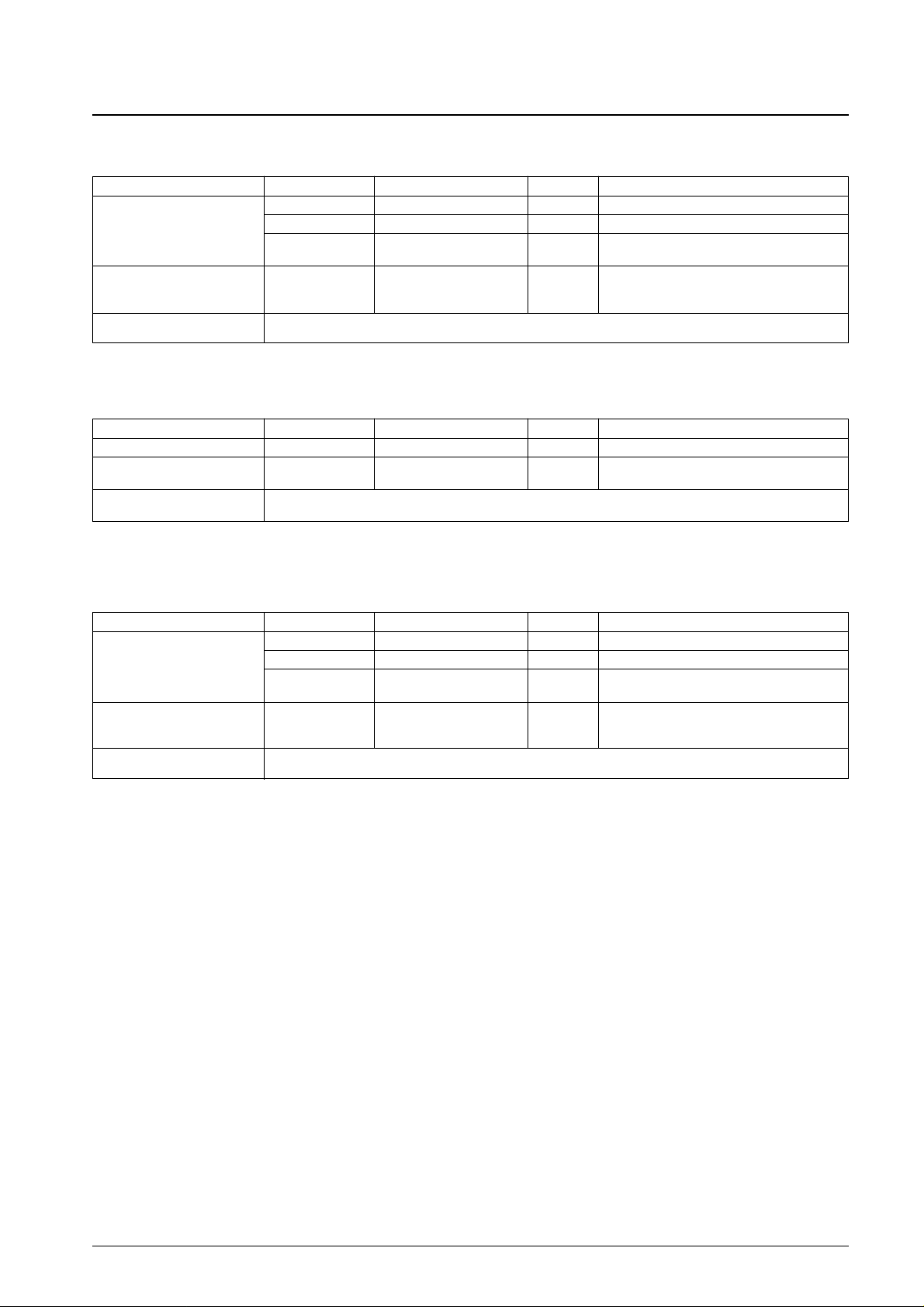
• Clock oscillator options to match application system
specifications.
— Oscillator circuit options: 2-pin ceramic oscillator (N,
F, and L versions)
— Divider circuit option: No divider, built-in divide-by-
three circuit, built-in divide-by-four circuit (N and L
versions)
• Supports continuous output of a square wave signal
(with a period 64 times the cycle time)
• Watchdog timer
— RC time constant scheme
— A watchdog timer function can be allocated to one of
the external pins as an option.
• EP version: LC65E1104, OTP version: LC65P1104
Page 2
Function Overview
Note: Sanyo will announce details on oscillator elements and oscillator circuit constants as recommended application circuits are developed. Customers
should check with Sanyo for the latest information as the development process progresses.
No. 5190-2/35
LC651204N/F/L, LC651202N/F/L
Item LC651204N/1202N LC651204F/1202F LC651204L/1202L
ROM
4096 × 8 bits (1204N) 4096 × 8 bits (1204F) 4096 × 8 bits (1204L)
Memory 2048 × 8 bits (1202N) 2048 × 8 bits (1202F) 2048 × 8 bits (1202L)
RAM 256 × 4 bits (1204/1202N) 256 × 4 bits (1204/1202F) 256 × 4 bits (1204/1202L)
Instruction
Instruction set 80 80 80
Table reference Supported Supported Supported
Interrupts 1 external, 1 internal 1 external, 1 internal 1 external, 1 internal
Timers 4-bit prescaler + 8-bit timer 4-bit prescaler + 8-bit timer 4-bit prescaler + 8-bit timer
Built-in functions Stack levels 8 8 8
Standby function
Supports standby mode entered Supports standby mode entered Supports standby mode entered
by the HALT instruction by the HALT instruction by the HALT instruction
Number of ports 22 I/O pins 22 I/O pins 22 I/O pins
Serial ports 4-bit or 8-bit I/O 4-bit or 8-bit I/O 4-bit or 8-bit I/O
I/O voltage 15 V max. 15 V max. 15 V max.
I/O ports Output current 10 mA typ. 20 mA max. 10 mA typ. 20 mA max. 10 mA typ. 20 mA max.
I/O circuit types Open drain (n-channel) or built-in pull-up resistor output selectable on a per-bit basis.
Output levels at reset High or low can be selected in port units. (ports C and D only)
Square wave output Supported Supported Supported
Minimum cycle time 2.77 µs (V
DD
≥ 3 V) 0.92 µs (VDD≥ 3 V) 3.84 µs (VDD≥ 2.5 V)
Characteristics Power-supply voltage 3 to 5.5 V 3 to 5.5 V 2.5 to 5.5 V
Power-supply current 1.5 mA typ. 2 mA typ. 1.5 mA typ.
Oscillator
Oscillator Ceramic (800 kHz, 1 MHz, 4 MHz) Ceramic (4 MHz) Ceramic (800 kHz, 1 MHz, 4 MHz)
Divider circuit option 1/1, 1/3, 1/4 1/1 1/1, 1/3, 1/4
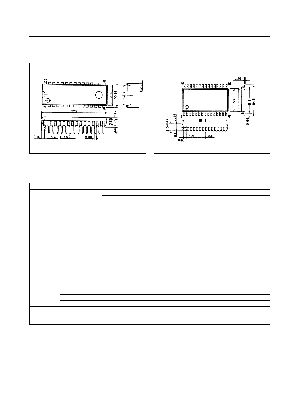
Other functions Package DIP30S-D MFP30S DIP30S-D MFP30S DIP30S-D MFP30S
SANYO: DIP30SD
[LC651204N/F/L, 651202N/F/L]
Note: The package drawings shown above are provided without error tolerances and are for reference purposes only. Contact Sanyo for official package
drawings.
SANYO: MFP30S
[LC651204N/F/L, 651202N/F/L]
Package Dimensions
unit : mm
3196-DIP30SD
unit : mm
3073A-MFP30S
Page 3
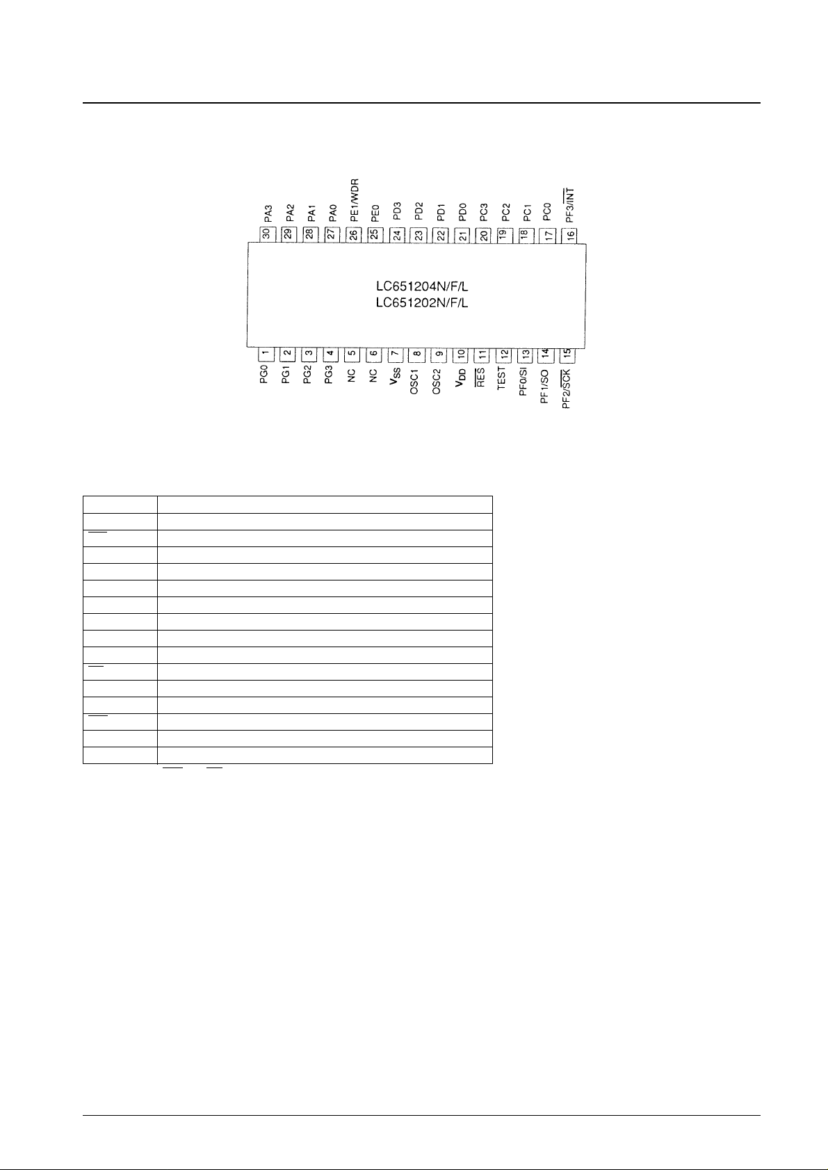
Pin Assignment
Common assignments for the DIP and MFP packages
Note: NC pins must be connected to VSS. Top view
Pin Functions
Note: The SI, SO, SCK, and INT pins are shared function pins that are also used as PF0 to PF3.
Pin Function
OSC1, OSC2 Connections for a ceramic oscillator element
RES Reset
PA0 to 3 I/O dual-function port A0 to A3
PC0 to 3 I/O dual-function port C0 to C3
PD0 to 3 I/O dual-function port D0 to D3
PE0 to 1 I/O dual-function port E0 to E1
PF0 to 3 I/O dual-function port F0 to F3
PG0 to 3 I/O dual-function port G0 to G3
TEST Test
INT Interrupt request
SI Serial input
SO Serial output
SCK Serial clock input and output
NC No connection
WDR Watchdog reset
No. 5190-3/35
LC651204N/F/L, LC651202N/F/L
Page 4
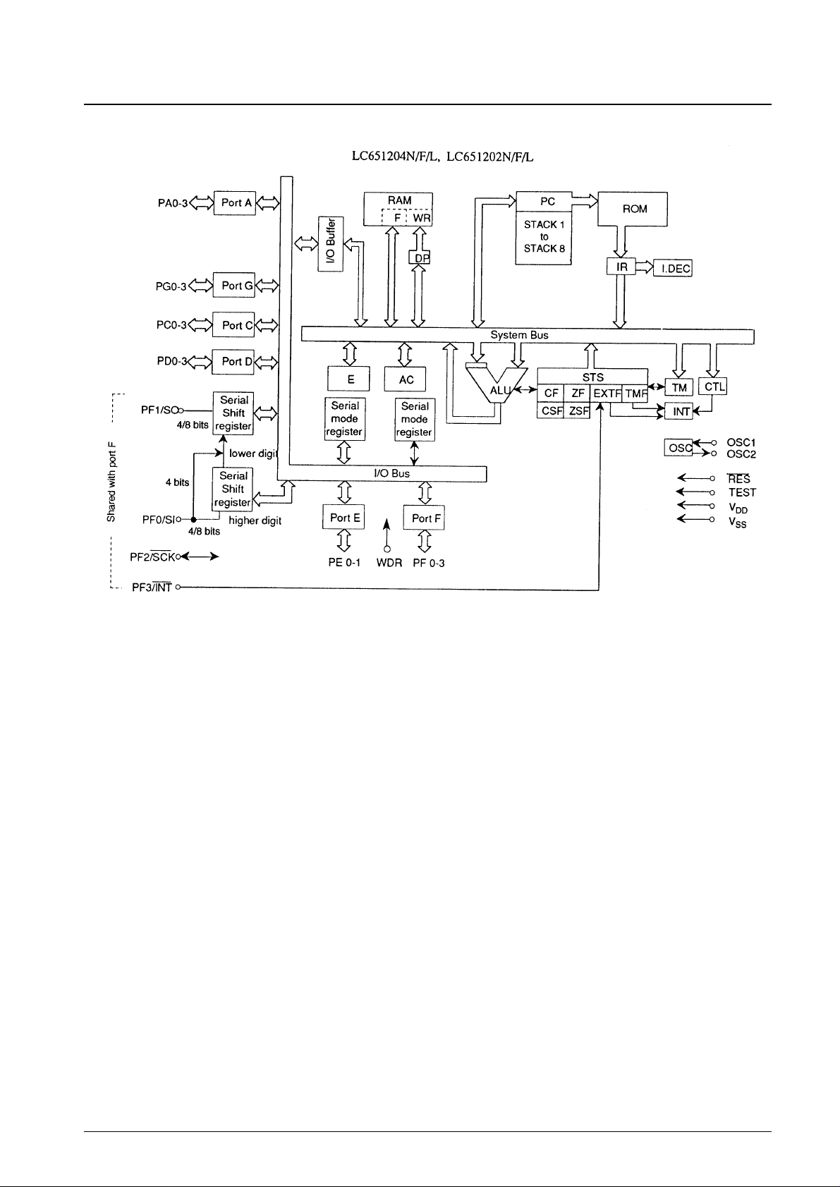
System Block Diagram
RAM: Data memory ROM: Program memory
F: Flag PC: Program counter
WR: Working register INT: Interrupt control
AC: Accumulator IR: Instruction register
ALU: Arithmetic and logic unit I.DEC: Instruction decoder
DP: Data pointer CF, CSF: Carry flag, carry save flag
E: E register ZF, ZSF: Zero flag, zero save flag
CTL: Control register EXTF: External interrupt request flag
OSC: Oscillator circuit TMF: Internal interrupt request flag
TM: Timer
STS: Status register
No. 5190-4/35
LC651204N/F/L, LC651202N/F/L
Page 5
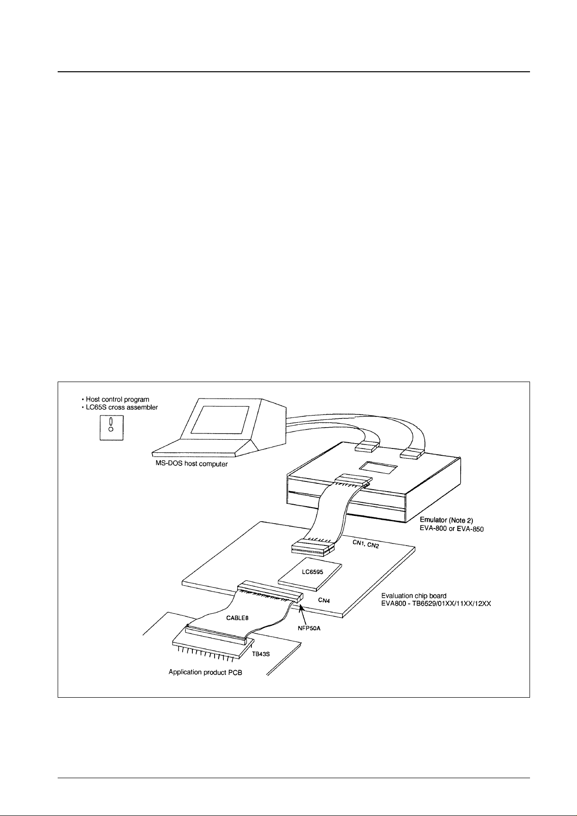
Development Support
Sanyo provides the following items to support application development using the LC651204 and LC651202.
1. User’s manual
The “LC651104/1102 User’s Manual” is used with these microcontrollers.
2. Development tool manual
See the “EVA800 - LC651104/1102 Development Tool Manual” for details on use of the EVA-800 system.
3. Development tool
• Program development (using the EVA-800 system)
— MS-DOS host computer system *1
— Cross assembler ... MS-DOS-based cross assembler: LC65S.EXE
— Evaluation chip: LC6595
— Emulator: The EVA-800 main unit plus the evaluation chip
• Program development (using the EVA-86000 system): Use the EVA86K-ECB651100.
• Program evaluation
The <LC65E1104> on-chip EPROM microcontroller
Development Support System
EVA-800 System
Note: 1. MS-DOS is a registered trademark of Microsoft Corporation
2. Here, “EVA-800” is a generic term for several emulators. Suffixes (A, B, etc.) will be attached to the name as new versions are developed. Note that
the EVA-800 emulator (i.e., the model with no suffix) is an old version and cannot be used.
No. 5190-5/35
LC651204N/F/L, LC651202N/F/L
Page 6

Pin Functions
No. 5190-6/35
Pin
V
DD
V
SS
OSC1
OSC2
PA0 to
PA3
PC0 to
PC3
PD0 to
PD3
Pin no.
1
1
1
1
4
4
4
I/O
—
—
Input
Output
I/O
I/O
I/O
Function
Power supply
• System clock oscillator
Connect an external ceramic oscillator
element to these pins
• Leave OSC2 open if an external clock
is supplied.
• I/O port A0 to A3
Input in 4-bit units using the IP
instruction
Output in 4-bit units using the OP
instruction
Port bits can be tested in bit units using
the BP and BNP instructions.
Port bits can be set or cleared in bit
units using the SPB and RPB
instructions.
• PA3 is used for standby control.
• Applications must be designed so that
no chattering (e.g. switch bounce)
occurs on the PA3 pin during a HALT
instruction execution cycle.
• I/O port C0 to C3
The PC0 to PC3 pin functions are
identical to those of the PA0 to 3 pins.*
• High or low can be specified as the
output at reset as an option.
Note: These pins do not have a
standby control function.
• I/O port D0 to D3
The PD0 to PD3 pin functions and
options are identical to those of the
PC0 to PC3 pins.
Options
—
(1) External clock
(2) Two-pin ceramic oscillator
(3) Divider circuit option
1. No divider circuit
2. Divide-by-three circuit
3. Divide-by-four circuit
(1) Output open drain
(2) Built-in pull-up resistor
• Options (1) and (2) can be
specified in bit units.
(1) Output open drain
(2) Built-in pull-up resistor
(3) High-level output at reset
(4) Low-level output at reset
• Options (1) and (2) can be
specified in bit units.
• Option (3) and (4) are
specified in 4-bit units.
The same as PC0 to PC3.
State at reset
—
—
High-level output
(i.e., the output
n-channel
transistor will be
off.)
• High-level
output
• Low-level
output
(Depending on
the option
specified.)
The same as
PC0 to PC3.
Handling when unused
—
—
Open drain output select
the options, connect to
V
SS
.
The same as PA0 to
PA3.
The same as PA0 to
PA3.
LC651204N/F/L, LC651202N/F/L
Continued on next page.
Page 7

No. 5190-7/35
LC651204N/F/L, LC651202N/F/L
Pin
PE0 to
PE1
/WDR
PF0/SI
PF1/SO
PF2/SCK
PF3/INT
PG0 to
PG3
NC
RES
TEST
Pin no.
2
4
4
2
1
1
I/O
I/O
I/O
I/O
Input
Input
Function
• I/O port E0 to E1
Input in 4-bit units using the IP
instruction
Output in 4-bit units using the OP
instruction
Port bits can be set or cleared in bit
units using the SPB and RPB
instructions.
Port bits can be tested in bit units using
the BP and BNP instructions.
• The PE0 pin also has a continuous
pulse (64·Tcyc) output function.
• The PE1 pin can be set to function as
the WDR watchdog timer reset pin as
an option.
• I/O port F0 to F3
This port has the same functions and
options as PE0 to PE1. *
• The pins PF0 to PF3 are also used as
the serial interface and the INT pin.
The function used can be selected
under program control.
SI ······Serial input port
SO·····Serial output port
SCK ··Serial clock input or output
INT····Interrupt request input
Serial I/O can be switched between 4bit and 8-bit operation under program
control.
Note: This port does not provide a
continuous pulse output function.
• I/O port G0 to G3
This port has the same functions and
options as PE0 to PE1. *
Note: This port does not provide a
continuous pulse output function.
• NC pin. This pin must be connected to
V
SS
in the EP and OTP versions.
• System reset input
• Connect an external capacitor for the
power up reset.
• A low level must be applied for at least
four clock cycles for the reset startup
sequence to operate correctly.
• LSI test pin
Must be connected to V
SS
.
Options
(1) Output open drain
(2) Built-in pull-up resistor
• Options (1) and (2) can be
specified in bit units.
(3) Normal port PE1
(4) Watchdog timer reset WDR
(5) (3) or (4) can be specified.
The same as PA0 to PA3.
The same as PA0 to PA3.
—
—
—
State at reset
High-level output
(i.e., the output
n-channel
transistor will be
off.)
The same as
PA0 to PA3.
The serial port
function is
disabled.
The interrupt
source is INT.
The same as
PA0 to PA3.
—
—
—
Handling when unused
The same as PA0 to
PA3.
The same as PA0 to
PA3.
The same as PA0 to
PA3.
Connect to V
SS
.
—
Must be connected to
V
SS
.
Continued from preceding page.
Page 8
Oscillator Circuit Options
Divider Options
Caution: The oscillator and divider options are summarized in the following tables. The information presented in those tables is crucial when using these
products.
No. 5190-8/35
LC651204N/F/L, LC651202N/F/L
Option Circuit Conditions and notes
The OSC2 pin must be left open.
External clock
Ceramic oscillator
Option Circuit Conditions and notes
• Supports both oscillator options.
• The oscillator frequency or the external clock
frequency must not exceed 1444 kHz
(LC651204N and LC651202N)
No divider (1/1) • The oscillator frequency or the external clock
frequency must not exceed 4330 kHz
(LC651204F and LC651202F)
• The oscillator frequency or the external clock
frequency must not exceed 1040 kHz
(LC651204L and LC651202L)
• Supports both oscillator options.
• The oscillator frequency or the external clock
frequency must not exceed 4330 kHz
Built-in divide-by-three circuit
• Supports both oscillator options.
• The oscillator frequency or the external clock
frequency must not exceed 4330 kHz
Built-in divide-by-four circuit
Page 9
Divider Options for the LC651204N/1202N, LC651204F/1202F, and LC651204L/1202L
LC651204N, LC651202N
No. 5190-9/35
LC651204N/F/L, LC651202N/F/L
Circuit type Frequency Divider option (cycle time) VDDrange Notes
800 kHz 1/1 (5 µs) 3 to 5.5 V
Ceramic oscillator
1 MHz 1/1 (4µs) 3 to 5.5 V
4 MHz
1/3 (3µs) 3 to 5.5 V This frequency cannot be used with the 1/1
1/4 (4µs) 3 to 5.5 V divider (i.e., no divider circuit) option.
External clock generated by a
670 k to 1444 kHz 1/1 (6 to 2.77 µs) 3 to 5.5 V
two-terminal RC oscillator circuit
2000 k to 4330 kHz 1/3 (6 to 2.77 µs) 3 to 5.5 V
2600 k to 4330 kHz 1/4 (6 to 3.70 µs) 3 to 5.5 V
Use of an external clock with the Driving the circuit with an external clock is not possible. To use external clock drive, specify the two-terminal RC
ceramic oscillator option selected oscillator option.
LC651204L LC651202L
Circuit type Frequency Divider option (cycle time) VDDrange Notes
800 kHz 1/1 (5 µs) 2.5 to 5.5 V
Ceramic oscillator
1 MHz 1/1 (4µs) 2.5 to 5.5 V
4 MHz 1/4 (4µs) 2.5 to 5.5 V
This frequency cannot be used with the 1/1, 1/3
divider (i.e., no divider circuit) option.
External clock generated by a
670 k to 1040 kHz 1/1 (6 to 3.84 µs) 2.5 to 5.5 V
two-terminal RC oscillator circuit
2000 k to 3120 kHz 1/3 (6 to 3.84 µs) 2.5 to 5.5 V
2600 k to 4160 kHz 1/4 (6 to 3.84 µs) 2.5 to 5.5 V
Use of an external clock with the Driving the circuit with an external clock is not possible. To use external clock drive, specify the two-terminal RC
ceramic oscillator option selected oscillator option.
LC651204F, LC651202F
Circuit type Frequency Divider option (cycle time) VDDrange Notes
Ceramic oscillator 4 MHz 1/1 (1 µs) 3 to 5.5 V
External clock generated by a
670 k to 4330 kHz 1/1 (6 to 0.92 µs) 3 to 5.5 V
two-terminal RC oscillator circuit
Use of an external clock with the Driving the circuit with an external clock is not possible. To use external clock drive, specify the two-terminal RC
ceramic oscillator circuit oscillator option.
Page 10

Port C and D Output State at Reset Options
The output levels at reset of the I/O ports C and D can be selected from the following two options, which are specified in
4-bit units.
Port Output Circuit Type Option
The output circuit types of the I/O ports can be selected from the following two options in bit units.
Watchdog Timer Reset Option
Whether the PE1/WDR pin functions as the normal port PE1 or as the WDR watchdog timer reset pin can be selected as
an option.
No. 5190-10/35
LC651204N/F/L, LC651202N/F/L
Option Conditions and notes
High-level output at reset Ports C and D in 4-bit units
Low-level output at reset Ports C and D in 4-bit units
Option Circuit Conditions and notes
Ports A, C, D, E, F, and G
Open drain output
Pull-up resistor output
Page 11
LC651204N, 651202N
Absolute Maximum Ratings at Ta = 25°C, VSS= 0 V
No. 5190-11/35
LC651204N/F/L, LC651202N/F/L
Parameter Symbol Conditions Applicable pins/notes Ratings Unit
Maximum supply voltage V
DD
max V
DD
–0.3 to +7.0 V
Voltages up to any
Output voltage V
O
OSC2 generated voltage are V
allowed.
Input voltage
VI(1) OSC1 *1 –0.3 to VDD+0.3 V
V
I
(2) TEST, RES –0.3 to VDD+0.3 V
V
IO
(1) PC0 to 3, PD0 to 3, PE0, 1, PF0 to 3 OD specification ports –0.3 to + 15 V
I/O voltage V
IO
(2) PC0 to 3, PD0 to 3, PE0, 1, PF0 to 3 PU specification ports –0.3 to VDD+0.3 V
V
IO
(3) PA0 to 3, PG0 to 3 –0.3 to VDD+0.3 V
Peak output current I
OP
I/O ports –2 to +20 mA
I
OA
Average value per pin over a 100-ms period I/O ports –2 to +20 mA
Σ IOA(1)
Total current for pins PC0 to 3, PD0 to 3, and
PC0 to PC3
PE0 to 1*2
PD0 to PD3 –15 to +100 mA
Average output current PE0 to PE1
Σ I
OA
(2)
Total current for pins PF0 to 3, PG0 to 3, and
PF0 to PF3
PA0 to 3*2
PG0 to PG3 –15 to +100 mA
PA0 to PA3
Allowable power Pd max (1) Ta = –40 to +85°C (DIP package) 250 mW
dissipation Pd max (2) Ta = –40 to +85°C (MFP package) 150 mW
Operating temperature Topr –40 to +85 °C
Storage temperature Tstg –55 to +125 °C
Allowable Operating Ranges at Ta = –40 to 85°C, VSS= 0 V, VDD= 3.0 to 5.5 V (unless otherwise specified)
Parameter Symbol Conditions Applicable pins/notes
Ratings
min typ max Unit
Operating power-supply
V
DD
V
DD
3.0 5.5 V
voltage
Standby power-supply
V
ST
RAM and register values retained *3 V
DD
1.8 5.5 V
voltage
VIH(1) Output n-channel transistors off
OD specification ports C, D, E,
0.7 V
DD
13.5 V
and F
VIH(2) Output n-channel transistors off
PU specification ports C, D, E,
0.7 V
DD
V
DD
V
and F
V
IH
(3) Output n-channel transistors off Port A, G 0.7 V
DD
V
DD
V
Input high-level voltage
V
IH
(4) Output n-channel transistors off
The INT, SCK, and SI pins with
0.8 V
DD
13.5 V
OD specifications
VIH(5) Output n-channel transistors off
The INT, SCK, and SI pins with
0.8 V
DD
V
DD
V
PU specifications
V
IH
(6) VDD= 1.8 to 5.5 V RES 0.8 V
DD
V
DD
V
V
IH
(7) External clock specifications OSC1 0.8 V
DD
V
DD
V
Continued on next page.
Page 12

No. 5190-12/35
LC651204N/F/L, LC651202N/F/L
Parameter Symbol Conditions Applicable pins/notes
Ratings
min typ max Unit
V
IL
(1) Output n-channel transistor off VDD= 4 to 5.5 V Port V
SS
0.2V
DD
V
V
IL
(2) Output n-channel transistor off VDD= 3 to 5.5 V Port V
SS
0.2V
DD
V
V
IL
(3) Output n-channel transistor off VDD= 4 to 5.5 V INT, SCk, SI V
SS
0.2V
DD
V
V
IL
(4) Output n-channel transistor off VDD= 3 to 5.5 V INT, SCk, SI V
SS
0.2V
DD
V
Input low-level voltage V
IL
(5) External clock specifications VDD= 4 to 5.5 V OSC1 V
SS
0.2V
DD
V
V
IL
(6) External clock specifications VDD= 3 to 5.5 V OSC1 V
SS
0.2V
DD
V
V
IL
(7) VDD= 4 to 5.5 V TEST V
SS
0.2V
DD
V
V
IL
(8) VDD= 3 to 5.5 V TEST V
SS
0.2V
DD
V
V
IL
(9) VDD= 4 to 5.5 V RES V
SS
0.2V
DD
V
V
IL
(10) VDD= 3 to 5.5 V RES V
SS
0.2V
DD
V
Frequencies up to 4.33 MHz
Operating frequency fop are supported if the divide-by-
V
DD
= 3 to 5.5 V
670 1444 kHz
(cycle time) (Tcyc) three or divide-by-four divider (6) (2.77) (µs)
circuit option is used.
External clock conditions
Figure 1. The divide-by-three
V
DD
= 3 to 5.5 V OSC1 670 4330 kHz
Frequency
text
or divide-by-four divider circuit
Pulse width textH, textL
option must be used if the
V
DD
= 3 to 5.5 V OSC1
69
ns
clock frequency exceeds
Rise and fall times textR, textF 1.444 MHz.
V
DD
= 3 to 5.5 V OSC1 50 ns
Guaranteed oscillator
See
constants Figure 2
Table 1.
Ceramic oscillator
Continued from preceding page.
Page 13

Electrical Characteristics at Ta = –40 to +85°C, VSS= 0 V, VDD= 3.0 to 5.5 V (unless otherwise specified)
No. 5190-13/35
LC651204N/F/L, LC651202N/F/L
Parameter Symbol Conditions Applicable pins/notes
Ratings
min typ max Unit
Output n-channel transistor off Ports C, D, E, and F
I
IH
(1) (Includes the n-channel transistor off leakage current.) with open-drain 5.0 µA
V
IN
= 13.5 V specifications
Input high-level current Output n-channel transistor off Ports A and G with
IIH(2) (Includes the n-channel transistor off leakage current.) open-drain 1.0 µA
V
IN
= V
DD
specifications
I
IH
(3) External clock mode, VIN= V
DD
OSC1 1.0 µA
I
IL
(1)
Output n-channel transistor off Ports with open-drain
–1.0 µA
V
IN
= V
SS
specifications
Input low-level current
I
IL
(2)
Output n-channel transistor off Ports with pull-up
–1.3 –0.35 mA
V
IN
= V
SS
resistor specifications
I
IL
(3) VIN= V
SS
RES –45 –10 µA
I
IL
(4) External clock mode, VIN= V
SS
OSC1 –1.0 µA
V
OH
(1)
I
OH
= –50 µA Ports with pull-up
VDD–1.2
V
Output high-level voltage
V
DD
= 4.0 to 5.5 V resistor specifications
V
OH
(2)
I
OH
= –10 µA Ports with pull-up
VDD–0.5
V
V
DD
= 3.0 to 5.5 V resistor specifications
V
OL
(1) IOL= 10 mA, VDD= 4.0 to 5.5 V Port 1.5 V
Output low-level voltage
V
OL
(2)
I
OL
= 1 mA, with the IOLfor all ports no more than
Port 0.5 V
1 mA. V
DD
= 3.0 to 5.5 V
Hysteresis voltage V
HIS
RES, INT, SCK,
0.1 V
DD
V
High-level threshold
V
tH
and SI OSC1 with
0.4 V
DD
0.8 V
DD
V
voltage
Schmitt specifications
Low-level threshold
V
tL
*4
0.2 V
DD
0.6 V
DD
V
voltage
Operating, output n-channel transistors off,
Current drain I
DDOP
(1) Ports = V
DD
V
DD
1.5 5 mA
Figure 2, 4 MHz, divide-by-three circuit
Ceramic oscillator I
DDOP
(2) Figure 2, 4 MHz, divide-by-four circuit V
DD
1.5 4 mA
I
DDOP
(3) Figure 2, 800 kHz V
DD
1.5 4 mA
670 to 1444 kHz, no divider circuit
External clock I
DDOP
(4) 2000 to 4330 kHz, divide-by-three circuit V
DD
1.5 5 mA
2600 to 4330 kHz, divide-by-four circuit
Standby mode I
DDst
Output n-channel transistor off, VDD= 5.5 V V
DD
0.05 10 µA
Ports = V
DD
, VDD= 3 V V
DD
0.025 5 µA
Schmitt characteristics
Continued on next page.
Page 14

No. 5190-14/35
LC651204N/F/L, LC651202N/F/L
Parameter Symbol Conditions Applicable pins/notes
Ratings
min typ max Unit
Oscillator characteristics
Ceramic oscillator
Oscillator frequency
f
CFOSC
*5
Figure 2, fo = 800 kHz OSC1, OSC2 768 800 832 kHz
Figure 2, fo = 1 MHz OSC1, OSC2 960 1000 1040 kHz
Figure 2, fo = 4 MHz, divide-by-three or divide-by-four OSC1, OSC2 3840 4000 4160 kHz
circuit
Oscillator stabilization
t
CFS
Figure 3, fo = 800 kHz, 1 MHz, 4 MHz
5 ms
time Divide-by-three or divide-by-four circuit
Pull-up resistors Output n-channel transistor off
I/O ports
R
PP
Vin= VSS, VDD= 5 V
Ports with pull-up
8 14 30 kΩ
resistor specifications
RES Ru V
in
= VSS, VDD= 5 V RES 100 250 400 kΩ
External reset
characteristics
Reset time t
RST
See
Figure 4.
f = 1 MHz
Pin capacitance Cp With all pins other than the pin being measured at 10 pF
V
IN
= V
SS
Serial clock
Input clock cycle time
t
CKCY
(1) Figure 5 SCK 3.0 µs
Output clock cycle time t
CKCY
(2) Figure 5 SCK
64×T
CYC
µs
*6
Input clock low-level
t
CKL
(1) Figure 5 SCK 1.0 µs
pulse width
Output clock low-level
t
CKL
(2) Figure 5 SCK
32×T
CYC
µs
pulse width
Input clock high-level
t
CKH
(1) Figure 5 SCK 1.0 µs
pulse width
Output clock high-level
t
CKH
(2) Figure 5 SCK
32×T
CYC
µs
pulse width
Continued from preceding page.
Continued on next page.
Page 15
No. 5190-15/35
LC651204N/F/L, LC651202N/F/L
Parameter Symbol Conditions Applicable pins/notes
Ratings
V
DD
(v) min typ max Unit
Serial input
Data setup time t
ICK
Stipulated with respect to the rising edge SI 0.4 µs
of SCK.
Data hold time t
CKI
Figure 5 SI 0.4 µs
Serial output
Stipulated with respect to the falling edge
of SCK.
Output delay time t
CKO
For n-channel open-drain outputs only:
SO 0.6 µs
External resistance: 1 kΩ, external
capacitance: 50 pF
Figure 5
Pulse output
Period
t
PCY
Figure 6
PE0
64 × T
CYC
µs
High-level pulse width
t
PH
Tcyc = 4 x the system clock period
PE0
32 × T
CYC
µs
For n-channel open-drain outputs only:
±10%
Low-level pulse width
t
PL
External resistance: 1 kΩ, external
PE0
32 × T
CYC
µscapacitance: 50 pF
±10%
C
W
When PE1 has open-drain output
WDR 0.1±5% µF
specifications
Guaranteed
R
W
When PE1 has open-drain output
WDR 680±1% kΩ
constants *7 specifications
3 to 5.5
R
l
When PE1 has open-drain output
WDR 100±1% Ω
specifications
Clear time (discharge) t
WCT
See Figure 7. WDR 100 µs
Clear period (charge) t
WCCY
See Figure 7. WDR 29 ms
C
W
When PE1 has open-drain output
WDR
0.047±5%
µF
specifications
Guaranteed
R
W
When PE1 has open-drain output
WDR 680±1% kΩ
constants *7 specifications
4 to 5.5
R
l
When PE1 has open-drain output
WDR 100±1% Ω
specifications
Clear time (discharge) t
WCT
See Figure 7. WDR 40 µs
Clear period (charge) t
WCCY
See Figure 7. WDR 15 ms
Watchdog timer
Note: 1. When driven internally using the oscillator circuit shown in Figure 3 with guaranteed constants, values up to the amplitude of the generated
oscillation are allowed.
2. The average over a 100-ms period
3. The operating power-supply voltage VDD must be maintained from the point where a HALT instruction is executed until the point where the device
has fully entered the standby state. Also, applications must be designed so that no chattering (e.g. switch bounce) occurs on the PA3 pin during a
HALT instruction execution cycle.
4. When external clock is selected as the oscillator option, the OSC1 pin has Schmitt characteristics.
5. The values shown for fCFOSC are the frequencies for which oscillation is possible. The center frequency when a ceramic oscillator is used may
differ by about 1% from the nominal value listed by the manufacturer of the ceramic oscillator element. See the specifications of the ceramic
oscillator element for details.
6. Tcyc = 4 × the system clock period
7. If this device is used in an environment subject to condensation, extra care is required concerning leakage between PE1 and adjacent pins and
leakage associated with external capacitors.
Continued from preceding page.
Page 16

Figure 1 External Clock Input Waveform
Figure 2 Ceramic Oscillator Circuit
No. 5190-16/35
LC651204N/F/L, LC651202N/F/L
Page 17

Figure 3 Oscillator Stabilization Period
Figure 4 Reset Circuit
Note: When the power supply rise time is zero, the reset time with
CRES = 0.1 µF will be between 5 and 50 ms.
If the power supply rise time is comparatively long, increase
the value of CRES so that the reset time is over 5 ms.
Table 1: Guaranteed Ceramic Oscillator Constants
No. 5190-17/35
LC651204N/F/L, LC651202N/F/L
4 MHz (Murata Mfg. Co., Ltd.)
C1 33 pF ± 10%
CSA4.00MG C2 33 pF ± 10%
CST4.00MGW (built-in capacitor version)
R 0 Ω
4 MHz (Kyocera Corporation)
C1 33 pF ± 10%
KBR4.0MSA C2 33 pF ± 10%
KBR4.0MKS (built-in capacitor version)
R 0 Ω
1 MHz (Murata Mfg. Co., Ltd.)
C1 100 pF ± 10%
CSB1000J
C2 100 pF ± 10%
R 2.2 kΩ
1 MHz (Kyocera Corporation)
C1 100 pF ± 10%
KBR1000F
C2 100 pF ± 10%
R 0 Ω
800 kHz (Murata Mfg. Co., Ltd.)
C1 100 pF ± 10%
CSB800J
C2 100 pF ± 10%
R 2.2 kΩ
800 kHz (Kyocera Corporation)
C1 220 pF ± 10%
KBR800F
C2 220 pF ± 10%
R 0 Ω
Page 18

No. 5190-18/35
LC651204N/F/L, LC651202N/F/L
Figure 5 Serial I/O Timing
Figure 6 Port PE0 Pulse Output Timing
With load conditions identical to those shown in Figure 5
Figure 7 Watchdog Timer Waveform
t
WCCY
: Charge time due to the external components CW, RW, and Rl.
t
WCT
: Discharge time due to program processing
Page 19

No. 5190-19/35
LC651204N/F/L, LC651202N/F/L
LC651204F, 651202F
Absolute Maximum Ratings at Ta = 25°C, VSS= 0 V
Parameter Symbol Conditions Applicable pins/notes Ratings Unit
Maximum supply voltage V
DD
max V
DD
–0.3 to +7.0 V
Voltages up to any
Output voltage V
O
OSC2 generated voltage are V
allowed.
Input voltage
VI(1) OSC1 *1 –0.3 to VDD+0.3 V
V
I
(2) TEST, RES –0.3 to VDD+0.3 V
V
IO
(1) PC0 to 3, PD0 to 3, PE0, 1, PF0 to 3 OD specification ports –0.3 to + 15 V
I/O voltage V
IO
(2) PC0 to 3, PD0 to 3, PE0, 1, PF0 to 3 PU specification ports –0.3 to VDD+0.3 V
V
IO
(3) PA0 to 3, PG0 to 3 –0.3 to VDD+0.3 V
Peak output current I
OP
I/O ports –2 to +20 mA
I
OA
Average value per pin over a 100-ms period I/O ports –2 to +20 mA
Total current for pins PC0 to 3, PD0 to 3, and
PC0 to 3
Σ I
OA
(1)
PE0 to 1 *2
PD0 to 3 –15 to +100 mA
Average output current PE0 to 1
Total current for pins PF0 to 3, PG0 to 3, and
PF0 to 3
Σ I
OA
(2)
PA0 to 3*2
PG0 to 3 –15 to +100 mA
PA0 to 3
Allowable power
Pd max (1) Ta = –40 to +85°C (DIP package) 250 mW
dissipation
Pd max (2) Ta = –40 to +85°C (MFP package) 150 mW
Operating temperature Topr –40 to +85 °C
Storage temperature Tstg –55 to +125 °C
Allowable Operating Ranges at Ta = –40 to +85°C, VSS= 0 V, VDD= 3.0 to 5.5 V (unless otherwise specified)
Parameter Symbol Conditions Applicable pins/notes
Ratings
min typ max Unit
Operating power-supply
V
DD
V
DD
3.0 5.5 V
voltage
Standby power-supply
V
ST
RAM and register values retained *3 V
DD
1.8 5.5 V
voltage
VIH(1) Output n-channel transistors off
OD specification ports C, D, E,
0.7 V
DD
13.5 V
and F
VIH(2) Output n-channel transistors off
PU specification ports C, D, E,
0.7 V
DD
V
DD
V
and F
V
IH
(3) Output n-channel transistors off Port A, G 0.7 V
DD
V
DD
V
Input high-level voltage
V
IH
(4) Output n-channel transistors off
The INT, SCK, and SI pins with
0.8 V
DD
13.5 V
OD specifications
VIH(5) Output n-channel transistors off
The INT, SCK, and SI pins with
0.8 V
DD
V
DD
V
PU specifications
V
IH
(6) VDD= 1.8 to 5.5 V RES 0.8 V
DD
V
DD
V
V
IH
(7) External clock specifications OSC1 0.8 V
DD
V
DD
V
V
IL
(1) Output n-channel transistors off Port V
SS
0.2 V
DD
V
V
IL
(2) Output n-channel transistors off INT, SCK, SI V
SS
0.2 V
DD
V
Input low-level voltage V
IL
(3) External clock specifications OSC1 V
SS
0.2 V
DD
V
V
IL
(4) TEST V
SS
0.2 V
DD
V
V
IL
(5) RES V
SS
0.2 V
DD
V
Continued on next page.
Page 20

No. 5190-20/35
LC651204N/F/L, LC651202N/F/L
Parameter Symbol Conditions Applicable pins/notes
Ratings
min typ max Unit
Operating frequency fop 670 4330 kHz
(cycle time) (T cyc) (6) (0.97) (µs)
External clock conditions
Frequency text OSC1 670 4330 kHz
Pulse width textH, textL Figure 1 OSC1 69 ns
Rise and fall times textR, textF OSC1 50 ns
Guaranteed oscillator
constants Figure 2 See table 1.
Ceramic oscillator
Electrical Characteristics at Ta = –40 to +85°C, VSS= 0 V, VDD= 3.0 to 5.5 V (unless otherwise specified)
Parameter Symbol Conditions Applicable pins/notes
Ratings
min typ max Unit
Output n-channel transistor off Ports C, D, E, and F
I
IH
(1) (Includes the n-channel transistor off leakage current.) with open-drain 5.0 µA
V
IN
= 13.5 V specifications
Input high-level current Output n-channel transistor off Ports A and G with
IIH(2) (Includes the n-channel transistor off leakage current.) open-drain 1.0 µA
V
IN
= V
DD
specifications
I
IH
(3) External clock mode, VIN= V
DD
OSC1 1.0 µA
I
IL
(1)
Output n-channel transistor off Ports with open-drain
–1.0 µA
V
IN
= V
SS
specifications
Input low-level current
I
IL
(2)
Output n-channel transistor off Ports with pull-up
–1.3 –0.35 mA
V
IN
= V
SS
resistor specifications
I
IL
(3) VIN= V
SS
RES –45 –10 µA
I
IL
(4) External clock mode, VIN= V
SS
OSC1 –1.0 µA
V
OH
(1) IOH= –50 µA
Ports with pull-up
VDD–1.2
V
Output high-level voltage
resistor specifications
VOH(2) IOH= –10 µA
Ports with pull-up
VDD–0.5
V
resistor specifications
V
OL
(1) IOL= 10 mA Port 1.5 V
Output low-level voltage
V
OL
(2)
I
OL
= 1 mA, with the IOLfor all ports no more than
Port 0.5 V
1 mA.
Hysteresis voltage V
HIS
RES, INT, SCK,
0.1 V
DD
V
High-level threshold
V
tH
and SI OSC1 with
0.4 V
DD
0.8 V
DD
V
voltage
Schmitt specifications
Low-level threshold
V
tL
*4
0.25V
DD
0.6 V
DD
V
voltage
Current drain
Ceramic oscillator
I
DDOP
(1) Figure 2, 4 MHz V
DD
2 6 mA
670 to 1444 kHz
External clock I
DDOP
(2) *1 Operating, output n-channel transistors off, V
DD
2 6 mA
Ports = V
DD
Standby mode I
DDst
Output n-channel transistor off,
V
DD
= 5.5 V V
DD
0.05 10 µA
Ports = V
DD
VDD= 3 V V
DD
0.025 5 µA
Schmitt characteristics
Continued from preceding page.
Continued on next page.
Page 21

No. 5190-21/35
LC651204N/F/L, LC651202N/F/L
Parameter Symbol Conditions Applicable pins/notes
Ratings
min typ max Unit
Oscillator characteristics
Ceramic oscillator
Oscillator frequency f
CFOSC
Figure 2, fo = 4 MHz *5 OSC1, OSC2 3840 4000 4160 kHz
Oscillator stabilization
t
CFS
Figure 3, fo = 4 MHz 5 ms
time
Pull-up resistors Output n-channel transistor off
I/O ports R
PP
Vin= VSS, VDD= 5 V Ports with pull-up 8 14 30 kΩ
resistor specifications
RES Ru Vin= VSS, VDD= 5 V RES 100 250 400 kΩ
External reset
characteristics
Reset time t
RST
See
Figure 4.
f = 1 MHz
Pin capacitance Cp With all pins other than the pin being measured at 10 pF
V
IN
= V
SS
Serial clock
Input clock cycle time
t
CKCY
(1) Figure 5 SCK 2.0 µs
Output clock cycle time
t
CKCY
(2) Figure 5 SCK
64 × T
CYC
µs
*6
Input clock low-level
t
CKL
(1) Figure 5 SCK 0.6 µs
pulse width
Output clock low-level
t
CKL
(2) Figure 5 SCK
32 × T
CYC
µs
pulse width
Input clock high-level
t
CKH
(1) Figure 5 SCK 0.6 µs
pulse width
Output clock high-level
t
CKH
(2) Figure 5 SCK
32 × T
CYC
µs
pulse width
Serial input
Data setup time
t
ICK
Stipulated with respect to the rising edge of SCK. SI 0.2 µs
Data hold time t
CKI
Figure 5 SI 0.2 µs
Serial output
Stipulated with respect to the falling edge of SCK.
Output delay time
t
CKO
For n-channel open-drain outputs only. External SO 0.4 µs
resistance: 1 kΩ, external capacitance: 50 pF. Figure 5
Pulse output
Period
t
PCY
Figure 6 PE0
64 × T
CYC
µs
Tcyc = 4 × the system clock period
PE0
32 × T
CYC
µsHigh-level pulse width t
PH
For n-channel open-drain outputs only:
±10%
External resistance: 1 kΩ, external capacitance: 50 pF
Low-level pulse width t
PL
PE0
32 × T
CYC
µs
±10%
Continued from preceding page.
Continued on next page.
Page 22

No. 5190-22/35
LC651204N/F/L, LC651202N/F/L
Parameter Symbol Conditions Applicable pins/notes
Ratings
V
DD
(v) min typ max Unit
C
W
When PE1 has open-drain output
WDR 0.01±5% µF
specifications
Guaranteed
R
W
When PE1 has open-drain output
WDR 680±1% kΩ
constants *7 specifications
3 to 5.5
R
l
When PE1 has open-drain output
WDR 100±1% Ω
specifications
Clear time (discharge) t
WCT
See Figure 7. WDR 10 µs
Clear period (charge) t
WCCY
See Figure 7. WDR 3.0 ms
C
W
When PE1 has open-drain output
WDR 0.01±5% µF
specifications
Guaranteed
R
W
When PE1 has open-drain output
WDR 680±1% kΩ
constants *7 specifications
R
l
When PE1 has open-drain output
4.5 to 5.5
WDR 100±1% Ω
specifications
Clear time (discharge) t
WCT
See Figure 7. WDR 10 µs
Clear period (charge) t
WCCY
See Figure 7. WDR 3.3 ms
Watchdog timer
Note: 1. When driven internally using the oscillator circuit shown in Figure 2 with guaranteed constants, values up to the amplitude of the generated
oscillation are allowed.
2. The average over a 100-ms period
3. The operating power-supply voltage V
DD
must be maintained from the point where a HALT instruction is executed until the point where the device
has fully entered the standby state. Also, applications must be designed so that no chattering (e.g. switch bounce) occurs on the PA3 pin during a
HALT instruction execution cycle.
4. When external clock is selected as the oscillator option, the OSC1 pin has Schmitt characteristics.
5. The values shown for f
CFOSC
are the frequencies for which oscillation is possible.
6. Tcyc = 4 × the system clock period
7. If this device is used in an environment subject to condensation, extra care is required concerning leakage between PE1 and adjacent pins and
leakage associated with external capacitors.
Continued from preceding page.
Page 23

No. 5190-23/35
LC651204N/F/L, LC651202N/F/L
Figure 1 External Clock Input Waveform
Figure 2 Ceramic Oscillator Circuit Figure 3 Oscillator Stabilization Period
Figure 4 Reset Circuit
Note: When the power supply rise time is zero, the reset time with
CRES = 0.1 µF will be between 5 and 50 ms.
If the power supply rise time is comparatively long, increase
the value of CRES so that the reset time is over 5 ms.
Table 1: Guaranteed Ceramic Oscillator Constants
4 MHz (Murata Mfg. Co., Ltd.)
C1 33 pF ± 10%
CSA4.00MG C2 33 pF ± 10%
CST4.00MGW (built-in capacitor version)
R 0 Ω
4 MHz (Kyocera Corporation)
C1 33 pF ± 10%
KBR4.0MSA C2 33 pF ± 10%
KBR4.0MKS (built-in capacitor version)
R 0 Ω
Page 24

No. 5190-24/35
LC651204N/F/L, LC651202N/F/L
Figure 5 Serial I/O Timing
Figure 6 Port PE0 Pulse Output Timing
With load conditions identical to those shown in Figure 5
Figure 7 Watchdog Timer Waveform
t
WCCY
: Charge time due to the external components CW, RW, and Rl.
t
WCT
: Discharge time due to program processing
Page 25

No. 5190-25/35
LC651204N/F/L, LC651202N/F/L
LC651204L, 651202L
Absolute Maximum Ratings at Ta = 25°C, VSS= 0 V
Parameter Symbol Conditions Applicable pins/notes Ratings Unit
Maximum supply voltage V
DD
max V
DD
–0.3 to +7.0 V
Voltages up to any
Output voltage V
O
OSC2 generated voltage are V
allowed.
Input voltage
VI(1) OSC1*1 –0.3 to VDD+0.3 V
V
I
(2) TEST, RES –0.3 to VDD+0.3 V
V
IO
(1) PC0 to 3, PD0 to 3, PE0, 1, PF0 to 3 OD specification ports –0.3 to + 15 V
I/O voltage V
IO
(2) PC0 to 3, PD0 to 3, PE0, 1, PF0 to 3 PU specification ports –0.3 to VDD+0.3 V
V
IO
(3) PA0 to 3, PG0 to 3 –0.3 to VDD+0.3 V
Peak output current I
OP
I/O ports –2 to +20 mA
I
OA
Average value per pin over a 100-ms period I/O ports –2 to +20 mA
Total current for pins PC0 to 3, PD0 to 3, and
PC0 to 3
Σ I
OA
(1)
PE0 to 1 *2
PD0 to 3 –15 to +100 mA
Average output current PE0 to 1
Total current for pins PF0 to 3, PG0 to 3, and
PF0 to 3
Σ I
OA
(2)
PA0 to 3 *2
PG0 to 3 –15 to +100 mA
PA0 to 3
Allowable power
Pd max (1) Ta = –40 to +85°C (DIP package) 250 mW
dissipation
Pd max (2) Ta = –40 to +85°C (MFP package) 150 mW
Operating temperature Topr –40 to +85 °C
Storage temperature Tstg –55 to +125 °C
Allowable Operating Ranges at Ta = –40 to +85°C, VSS= 0 V, VDD= 2.5 to 5.5 V (unless otherwise specified)
Parameter Symbol Conditions Applicable pins/notes
Ratings
min typ max Unit
Operating power-supply
V
DD
V
DD
2.5 5.5 V
voltage
Standby power-supply
V
ST
RAM and register values retained *3 V
DD
1.8 5.5 V
voltage
VIH(1) Output n-channel transistors off
OD specification ports C, D, E,
0.7 V
DD
13.5 V
and F
VIH(2) Output n-channel transistors off
PU specification ports C, D, E,
0.7 V
DD
V
DD
V
and F
V
IH
(3) Output n-channel transistors off Port A, G 0.7 V
DD
V
DD
V
Input high-level voltage
V
IH
(4) Output n-channel transistors off
The INT, SCK, and SI pins with
0.8 V
DD
13.5 V
OD specifications
VIH(5) Output n-channel transistors off
The INT, SCK, and SI pins with
0.8 V
DD
V
DD
V
PU specifications
V
IH
(6) VDD= 1.8 to 5.5 V RES 0.8 V
DD
V
DD
V
V
IH
(7) External clock specifications OSC1 0.8 V
DD
V
DD
V
V
IL
(1) Output n-channel transistors off Port V
SS
0.2 V
DD
V
V
IL
(2) Output n-channel transistors off INT, SCK, SI V
SS
0.15 VDDV
Input low-level voltage V
IL
(3) External clock specifications OSC1 V
SS
0.15 VDDV
V
IL
(4) TEST V
SS
0.2 V
DD
V
V
IL
(5) RES V
SS
0.15 VDDV
Page 26

No. 5190-26/35
LC651204N/F/L, LC651202N/F/L
Parameter Symbol Conditions Applicable pins/notes
Ratings
min typ max Unit
Operating frequency fop Frequencies up to 4.16 MHz are supported if the 670 1040 kHz
(cycle time) (Tcyc) divide-by-four divider circuit option is used. (6) (3.84) (µs)
External clock conditions Figure 1. The divide-by- three or divide-by-four
Frequency text divider circuit option must be used if the clock OSC1 670 4160 kHz
Pulse width textH, textL frequency exceeds 1.040 MHz. OSC1 150 ns
Rise and fall times textR, textF OSC1 100 ns
Guaranteed oscillator
constants Figure 2 See table 1.
Ceramic oscillator
Electrical Characteristics at Ta = –40 to +85°C, VSS= 0 V, VDD= 2.5 to 5.5 V (unless otherwise specified)
Parameter Symbol Conditions Applicable pins/notes
Ratings
min typ max Unit
Output n-channel transistor off Ports C, D, E, and F
I
IH
(1) (Includes the n-channel transistor off leakage current.) with open drain 5.0 µA
V
IN
= 13.5 V specifications
Input high-level current Output n-channel transistor off Ports A and G with
IIH(2) (Includes the n-channel transistor off leakage current.) open drain 1.0 µA
V
IN
= V
DD
specifications
I
IH
(3) External clock mode, VIN= V
DD
OSC1 1.0 µA
I
IL
(1)
Output n-channel transistor off Ports with open drain
–1.0 µA
V
IN
= V
SS
specifications
Input low-level current
I
IL
(2)
Output n-channel transistor off Ports with pull-up
–1.3 –0.35 mA
V
IN
= V
SS
resistor specifications
I
IL
(3) VIN= V
SS
RES –45 –10 µA
I
IL
(4) External clock mode, VIN= V
SS
OSC1 –1.0 µA
Output high-level voltage
V
OH
(1) IOH= –10 µA
Ports with pull-up
VDD–0.5
V
resistor specifications
V
OL
(1) IOL= 3 mA Port 1.5 V
Output low-level voltage
V
OL
(2)
I
OL
= 1 mA, with the IOLfor all ports no more than
Port 0.4 V
1 mA.
Hysteresis voltage V
HIS
RES, INT, SCK,
0.1 V
DD
V
High-level threshold
V
tH
and SI OSC1 with
0.4 V
DD
0.8 V
DD
V
voltage
Schmitt specifications
Low-level threshold
V
tL
*4
0.2 V
DD
0.6 V
DD
V
voltage
Schmitt characteristics
Continued from preceding page.
Continued on next page.
Page 27

No. 5190-27/35
LC651204N/F/L, LC651202N/F/L
Parameter Symbol Conditions Applicable pins/notes
Ratings
min typ max Unit
Current drain Operating, output n-channel transistors off,
I
DDOP
(1) Ports = V
DD
V
DD
1.5 4 mA
Ceramic oscillator Figure 2, 4 MHz, divide-by-four circuit
I
DDOP
(2) Figure 2, 4 MHz, divide-by-four circuit VDD= 2.5 V V
DD
0.5 1 mA
I
DDOP
(3) Figure 2, 800 kHz V
DD
1.5 4.0 mA
670 to 1024 kHz, no divider circuit
External clock I
DDOP
(4) 2000 to 3120 kHz, divide-by-three circuit V
DD
1.5 4 mA
2600 to 4160 kHz, divide-by-four circuit
Standby mode I
DDst
Output n-channel transistor off,
V
DD
= 5.5 V V
DD
0.05 10 µA
Ports = V
DD
VDD= 2.5 V V
DD
0.020 4 µA
Oscillator characteristics
Ceramic oscillator
Oscillator frequency f
CFOSC
Figure 2, fo = 800 kHz OSC1, OSC2 768 800 832 kHz
*5 Figure 2, fo = 1 MHz OSC1, OSC2 960 1000 1040 kHz
Figure 2, fo = 4 MHz, divide-by-four circuit OSC1, OSC2 3840 4000 4160 kHz
Oscillator stabilization
t
CFS
Figure 3, fo = 800 kHz, 1 MHz,
5 ms
time 4 MHz, divide-by-four circuit
Pull-up resistors
Output n-channel transistor off
I/O ports R
PP
Vin= VSS, VDD= 5 V
Ports with pull-up
8 14 30 kΩ
resistor specifications
RES Ru V
in
= VSS, VDD= 5 V RES 100 250 400 kΩ
External reset
characteristics
Reset time t
RST
See Figure 4.
f = 1 MHz
Pin capacitance Cp With all pins other than the pin being measured at 10 pF
V
IN
= V
SS
Continued from preceding page.
Continued on next page.
Page 28

No. 5190-28/35
LC651204N/F/L, LC651202N/F/L
Parameter Symbol Conditions Applicable pins/notes
Ratings
min typ max Unit
Serial clock
Input clock cycle time
t
CKCY
(1) Figure 5 SCK 6.0 µs
Output clock cycle time t
CKCY
(2) Figure 5 SCK
64 × T
CYC
µs
*6
Input clock low-level
t
CKL
(1) Figure 5 SCK 2.0 µs
pulse width
Output clock low-level
t
CKL
(2) Figure 5 SCK
32 × T
CYC
µs
pulse width
Input clock high-level
t
CKH
(1) Figure 5 SCK 2.0 µs
pulse width
Output clock high-level
t
CKH
(2) Figure 5 SCK
32 × T
CYC
µs
pulse width
Serial input
Data setup time
t
ICK
Stipulated with respect to the rising edge of SCK. SI 0.5 µs
Data hold time t
CKI
Figure 5 SI 0.5 µs
Serial output Stipulated with respect to the falling edge of SCK.
Output delay time t
CKO
For n-channel open-drain outputs only: External
SO 1.0 µs
resistance: 1 kΩ, external capacitance: 50 pF. Figure 5
Pulse output period t
PCY
Figure 6 PE0
64 × T
CYC
µs
Tcyc = 4 × the system clock period
PE0
32 × T
CYC
µs
High-level pulse width t
PH
For n-channel open-drain outputs only:
±10%
External resistance: 1 kΩ, external capacitance: 50 pF
Low-level pulse width t
PL
PE0
32 × T
CYC
µs
±10%
Continued from preceding page.
Continued on next page.
Page 29

No. 5190-29/35
LC651204N/F/L, LC651202N/F/L
Parameter Symbol Conditions Applicable pins/notes
Ratings
V
DD
(v) min typ max Unit
C
W
When PE1 has open-drain output
WDR 0.1±5% µF
specifications
Guaranteed
R
W
When PE1 has open-drain output
WDR 680±1% kΩ
constants *7 specifications
2.5 to 5.5
R
l
When PE1 has open-drain output
WDR 100±1% Ω
specifications
Clear time (discharge) t
WCT
See Figure 7. WDR 100 µs
Clear period (charge) t
WCCY
See Figure 7. WDR 26 ms
C
W
When PE1 has open-drain output
WDR
0.047±5%
µF
specifications
Guaranteed
R
W
When PE1 has open-drain output
WDR 680±1% kΩ
constants *7 specifications
R
l
When PE1 has open-drain output
2.5 to 5.5
WDR 100±1% Ω
specifications
Clear time (discharge) t
WCT
See Figure 7. WDR 40 µs
Clear period (charge) t
WCCY
See Figure 7. WDR 12 ms
Watchdog timer
Note: 1. When driven internally using the oscillator circuit shown in Figure 2 with guaranteed constants, values up to the amplitude of the generated
oscillation are allowed.
2. The average over a 100-ms period
3. The operating power-supply voltage V
DD
must be maintained from the point where a HALT instruction is executed until the point where the device
has fully entered the standby state. Also, applications must be designed so that no chattering (e.g. switch bounce) occurs on the PA3 pin during a
HALT instruction execution cycle.
4. When external clock is selected as the oscillator option, the OSC1 pin has Schmitt characteristics.
5. The values shown for f
CFOSC
are the frequencies for which oscillation is possible.
6. T
cyc
= 4 × the system clock period
7. If this device is used in an environment subject to condensation, extra care is required concerning leakage between PE1 and adjacent pins and
leakage associated with external capacitors.
Continued from preceding page.
Page 30

No. 5190-30/35
LC651204N/F/L, LC651202N/F/L
Figure 1 External Clock Input Waveform
Figure 2 Ceramic Oscillator Circuit
Figure 3 Oscillator Stabilization Period
Page 31

No. 5190-31/35
LC651204N/F/L, LC651202N/F/L
Figure 5 Serial I/O Timing
Figure 4 Reset Circuit
Note: When the power supply rise time is zero, the reset time with
CRES = 0.1 µF will be between 5 and 50 ms.
If the power supply rise time is comparatively long, increase
the value of CRES so that the reset time is over 5 ms.
Table 1: Guaranteed Ceramic Oscillator Constants
4 MHz (Murata Mfg. Co., Ltd.)
C1 33 pF ± 10%
CSA4.00MGU C2 33 pF ± 10%
CST4.0MGWU (built-in capacitor version)
R 0 Ω
1 MHz (Murata Mfg. Co., Ltd.)
C1 100 pF ± 10%
CSB1000J
C2 100 pF ± 10%
R 2.2 kΩ
1 MHz (Kyocera Corporation)
C1 100 pF ± 10%
KBR1000F
C2 100 pF ± 10%
R 0 Ω
800 kHz (Murata Mfg. Co., Ltd.)
C1 100 pF ± 10%
CSB800J
C2 100 pF ± 10%
R 2.2 kΩ
800 kHz (Kyocera Corporation)
C1 220 pF ± 10%
KBR800F
C2 220 pF ± 10%
R 0 Ω
Figure 6 Port PE0 Pulse Output Timing
With load conditions identical to those shown in Figure 5
Page 32

No. 5190-32/35
LC651204N/F/L, LC651202N/F/L
Figure 7 Watchdog Timer Waveform
t
WCCY
: Charge time due to the external components CW, RW, and Rl
t
WCT
: Discharge time due to program processing
Page 33

LC651204/1202 Instruction Set (by function)
Abbreviations
AC: Accumulator M: Memory ZF : Zero flag
ACt: Accumulator bit t M(DP): Memory addressed by DP ( )[ ] : Indicates the contents of the item enclosed.
CF: Carry flag P(DPL): I/O port specified by DPL ← : Transfer and direction
CTL: Control register PC: Program counter + : Addition
DP: Data pointer STACK: Stack pointer – : Subtraction
E: E register TM: Timer ^ : Logical AND
EXTF: External interrupt request flag TMF: Timer (internal) interrupt request flag ∨ : Logical OR
Fn: Flag bit n At, Ha, La:Working registers ∨ : Logical exclusive OR
No. 5190-33/35
LC651204N/F/L, LC651202N/F/L
Instruction code Modified
Mnemonic Operation Description status Notes
D
7D6D5D4D3D2D1D0
flags
CLA Clear AC 1 1 0 0 0 0 0 0 1 1 AC ← 0 Clears AC. ZF *1
ClC Clear CF 1 1 1 0 0 0 0 1 1 1 CF ← 0 Clears CF. CF
STC Set CF 1 1 1 1 0 0 0 1 1 1 CF ← 1 Sets CF. CF
CMA Complement AC 1 1 1 0 1 0 1 1 1 1 AC ← (AC) Sets AC to the one's ZF
INC Increment AC 0 0 0 0 1 1 1 0 1 1 AC ← (AC) + 1 Increments AC. ZF CF
DEC Decrement AC 0 0 0 0 1 1 1 1 1 1 AC ← (AC) – 1 Decrements AC. ZF CF
RAL Rotate AC left through CF 0 0 0 0 0 0 0 1 1 1
AC
0
← (CF), AC
n+1
Shifts AC together with CF left.
ZF CF
← (ACn), CF ← (AC3)
TAE Transfer AC to E 0 0 0 0 0 0 1 1 1 1 E ← (AC)
Moves the contents of AC to E.
XAE Exchange AC with E 0 0 0 0 1 1 0 1 1 1 (AC) ↔ (E)
Exchanges the contents of AC and E.
INM Increment M 0 0 1 0 1 1 1 0 1 1 M(DP) ← [M(DP)] + 1 Increments M(DP). ZF CF
DEm Decrement M 0 0 1 0 1 1 1 1 1 1 M(DP) ← [M(DP)] – 1 Decrements M(DP). ZF CF
SmB bit Set M data bit 0 0 0 0 1 0 B1B01 1 M(DP, B1B0) ← 1
Sets the bit in M(DP) specified
by B1B0 to 1.
RMB bit Reset M data bit 0 0 1 0 1 0 B1B01 1 M(DP, B1B0) ← 0
Clears the bit in M(DP) specified
by B1B0 to 0.
AD Add M to AC 0 1 1 0 0 0 0 0 1 1 AC ← (AC) + [M(DP)]
Adds the contents of AC and
M(DP) as two's complement
ZF CF
quantities and stores the result
in AC.
ADC Add M to AC with CF 0 0 1 0 0 0 0 0 1 1
AC ← (AC) + [M(DP)]
Adds the contents of AC, CF,
+ (CF)
and M(DP) as two's complement
ZF CF
quantities and stores the result
in AC.
DAA Decimal adjust AC in addition 1 1 1 0 0 1 1 0 1 1 AC ← (AC) + 3 Adds 6 to AC. ZF
DAS
Decimal adjust AC in subtraction
1 1 1 0 1 0 1 0 1 1 AC ← (AC) + 10 Adds 10 to AC. ZF
Takes the logical exclusive OR ZF
EXL Exclusive or M to AC 1 1 1 1 0 1 0 1 1 1 AC ← (AC) ∨ [M(DP)] of AC and M(DP) and stores
the result in AC.
Takes the logical AND of AC
AND And M to AC 1 1 1 0 0 1 1 1 1 1 AC ← (AC) ^ [M(DP)] and M(DP) and stores the ZF
result in AC.
OR Or M to AC 1 1 1 0 0 1 0 1 1 1 AC ← (AC) ∨ [M(DP)]
Takes the logical OR of AC and
ZF
M(DP) and stores the result in AC.
Compares the contents of AC
CM Compare AC with M 1 1 1 1 1 0 1 1 1 1 [M(DP)] + (AC) + 1
and M(DP) and sets or clears
CF and ZF accordingly.
ZF CF
Compares the contents of AC
and the immediate data I3I2I1I
0
and sets or clears CF and ZF
accordingly.
Cl data
Compare AC with 0 0 1 0 1 1 0 0
2 2 I
3I2I1I0
+ (AC) + 1 ZF CF
immediate data 0 1 0 0 I
3I2I1I0
CLI data
Compare DPLwith immediate 0 0 1 0 1 1 0 0
2 2 (DPL) ∨ I3I2I1I
0
Compares the contents of DPL
ZF
data 0 1 0 1 I3I2I1I
0
and the immediate data.
LI data Load AC with immediate data 1 1 0 0 I3I2I1I01 1 AC ← I3I2I1I
0
Loads AC with the immediate
ZF
*1
data I3I2I1I0.
S Store AC to M 0 0 0 0 0 0 1 0 1 1 M(DP) ← (AC)
Stores the contents of AC at M(DP).
L Load AC from M 0 0 1 0 0 0 0 1 1 1 AC ← [M(DP)]
Loads the contents of M(DP) into AC.
ZF
Exchange AC with M then
1 0 1 0 0 M2M1M01 2
(AC) ↔ [M(DP)]
Exchanges the contents of AC
XM data modify DPHwith immediate DPH← (DPH) ∨
and M(DP). Then, replaces the
ZF
data 0 M2M1M
0
contents of DPH with (DPH) ∨ 0
M2M1M0.
Exchanges the contents of AC
X Exchange AC with M 1 0 1 0 0 0 0 0 1 2 (AC) ↔ [M(DP)]
and M(DP).
ZF
Exchange AC with M then
1 1 1 1 1 1 1 0 1 2
(AC) ↔ [M(DP)]
Exchanges the contents of AC
XI
increment DP
L
DPL← (DPL) + 1
and M(DP). Then, increments ZF
the contents of DPL.
XD
Exchange AC with M then
1 1 1 1 1 1 1 1 1 2
(AC) ↔ [M(DP)]
Exchanges the contents of AC
Decrement DP
L
DPL← (DPL) – 1
and M(DP). Then, Decrements ZF
the contents of DP
L
.
Loads into AC and E the ROM
RTBl
Read table data from
0 1 1 0 0 0 1 1 1 2
AC, E ↔ ROM data stored at the location given
program ROM (PCh, E, AC) by the lower 8 bits of the PC, E
and AC.
Instruction groupAccumulator manipulation instructions
Arithmetic and comparison instructionsLoad and store instructions
Memory manipulation
instructions
Number of bytes
ZF is set to indicate
the result of the
(DPH) ∨ 0 M2M1M
0
operation.
ZF is set according
to the contents of
DPH at the point the
instruction was
executed.
ZF is set to indicate
the result of the DP
L
+1 operation.
ZF is set to indicate
the result of the DP
L
–1 operation.
Number of cycles
Magnitude relationship
CF ZF
[M(DP)] > (AC) 0 0
[M(DP)] = (AC) 1 1
[M(DP)] < (AC) 1 0
Magnitude relationship
CF ZF
I3I2I1I0 > (AC) 0 0
I3I2I1I0 = (AC) 1 1
I
3I2I1
I0 < (AC) 1 0
Continued on next page.
Page 34

No. 5190-34/35
LC651204N/F/L, LC651202N/F/L
Instruction code
Modified
Mnemonic Operation Description status Notes
D
7D6D5D4D3D2D1D0
flags
Load DPHwith Zero and
DPH← 0 Loads 0 into DPHand the
LDZ data DP
L
with immediate data 1 0 0 0 I3I2I1I01 1
DPL← I3I2I1I
0
immediate data I3I2I1I0 into DPL.
respectively
LHI data
Load DPH with immediate
0 1 0 0 I
3I2I1I0
1 1 DPH← I3I2I1I
0
Loads the immediate data
I3I2I1I
0
data into DPH.
IND Increment DP
L
1 1 1 0 1 1 1 0 1 1 DPL← (DPL) + 1 Increments the contents of DPL. ZF
DED Decrement DP
L
1 1 1 0 1 1 1 1 1 1 DPL← (DPL) – 1 Decrements the contents of DPL. ZF
TAL Transfer AC to DP
L
1 1 1 1 0 1 1 1 1 1 DPL← (AC)
Moves the contents of AC to DPL.
TLA Transfer DPL to AC 1 1 1 0 1 0 0 1 1 1 AC ← (DPL)
Moves the contents of DPL to AC.
ZF
XAH Exchange AC with DPH 0 0 1 0 0 0 1 1 1 1 (AC) ↔ (DPH)
Exchanges the contents of AC
and DP
H
.
XAt t1 t0 Exchanges the contents of AC
XA0
Exchange AC with working
1 1 1 0 0 0 0 0 1 1 (AC) ↔ (A0) and the working register A0, A1,
XA1
register At
1 1 1 0 0 1 0 0 1 1 (AC) ↔ (A1) A2, or A3 specified by t1t0.
XA2 1 1 1 0 1 0 0 0 1 1 (AC) ↔ (A2)
XA3 1 1 1 0 1 1 0 0 1 1 (AC) ↔ (A3)
XHa
Exchange DPH with working
a Exchanges the contents of DP
H
XH0
register Ha
1 1 1 1 1 0 0 0 1 1 (DPH) ↔ (H0) and the working register H0 or H1
XH1 1 1 1 1 1 1 0 0 1 1 (DPH) ↔ (H1) specified by a.
XLa
Exchange DPH with working
a Exchanges the contents of DP
L
XL0
register Ha
1 1 1 1 1 0 0 0 1 1 (DPL) ↔ (L0) and the working register L0 or L1
XL1 1 1 1 1 1 1 0 0 1 1 (DPL) ↔ (L1) specified by a.
SFB flag Set flag bit 0 1 0 1 B3B2B1B01 1 Fn ← 1
Sets the flag specified by B3B
2
B1B0to 1.
Clears the flag specified by B
3
B2B1B0to 0.
RFB flag Reset flag bit 0 0 0 1 B3B2B1B01 1 Fn ← 0
ZF
0 1 1 0 1 P10P9P
8
PC ← P10P9P8P7P6Jumps to the location specified
JMP addr Jumping in the current bank
P
7P6P5P4P3P2P1P0
2 2 P5P4P3P2P1P0by the immediate data P10P
9
P8P7P6P5P4P3P2P1P0.
JPEA
Jumping current page
1 1 1 1 1 0 1 0 1 1 PC
0
to 7← (E, AC)
Jumps to the location given by
modified by E and AC
replacing the lower 8 bits of the
PC with E and AC.
CZP addr
Call subroutine in the zero
1 0 1 1 P3P2P1P01 1
STACK ← (PC) + 1
page
PC10to 6, PC1to 0← 0
Calls a subroutine on page 0.
PC5to 2← P3P2P1P
0
CAL addr Call subroutine 1 0 1 0 1 P10P9P82 2 STACK ← (PC) + 2 Calls a subroutine.
RT Return from subroutine 0 1 1 0 0 0 1 0 1 1 PC ← (STACK) Returns from a subroutine.
RTI Return from interrupt routine 0 0 1 0 0 0 1 0 1 1
PC ← (STACK) Returns from an interrupt
ZF CF
CF, ZF ← CSF, ZSF handling routine.
Specifies a pseudo I/O port
BANK Change bank 1 1 1 1 1 1 0 1 1 1
and changes the bank.
BAt addr Change bank
0 1 1 1 0 0 t
1t0
2 2
PC7to 0← P7P6P5P4Branches to the location on the
P7P6P5P4P3P2P1P
0
P3P2P1P0same page specified by P7to P
0
if ACt = 1 if the bit in AC specified by the
immediate data t1t0 is 1.
BNAt addr Branch on no AC bit
0 0 1 1 0 0 t1t
0
2 2
PC7to 0← P7P6P5P4Branches to the location on the
P7P6P5P4P3P2P1P
0
P3P2P1P0same page specified by P7to P
0
if ACt = 0 if the bit in AC specified by the
immediate data t1t0 is 0.
BMt addr Branch on M bit
0 1 1 1 0 1 t1t
0
2 2
PC7to 0← P7P6P5P4Branches to the location on the
P7P6P5P4P3P2P1P
0
P3P2P1P0same page specified by P7to P
0
if [M(DP, t1t0)] = 1 if the bit in M(DP) specified by
the immediate data t
1t0
is 1.
BNMt addr Branch on no M bit
0 0 1 1 0 1 t
1t0
2 2
PC7to 0← P7P6P5P4Branches to the location on the
P7P6P5P4P3P2P1P
0
P3P2P1P0same page specified by P7to P
0
if [M(DP, t1t0)] = 0 if the bit in M(DP) specified by
the immediate data t
1t0
is 0.
BPt addr Branch on Port bit
0 1 1 1 1 0 t
1t0
2 2
PC7to 0← P7P6P5P4Branches to the location on the
P7P6P5P4P3P2P1P
0
P3P2P1P0same page specified by P7to P
0
if [P(DPL, t1t0)] = 1 if the bit in port P(DPL) specified
by the immediate data t
1t0
is 1.
BNPt addr Branch on no Port bit
0 0 1 1 1 0 t1t
0
2 2
PC7to 0← P7P6P5P4Branches to the location on the
P
7P6P5P4P3P2P1P0
P3P2P1P0same page specified by P7to P
0
if [P(DPL, t1t0)] = 0 if the bit in port P(DPL) specified
by the immediate data t
1t0
is 0.
0 1 1 1 1 0 0 0
PC7to 0← P7P6P5P4Branches to the location on the
BTM addr Branch on timer
P
7P6P5P4P3P2P1P0
P3P2P1P0same page specified by P7to P
0
TMF
2 2
if TMF = 0 if TMF is 1. Also clears TMF.
then TMF ← 0
Instruction group
Data pointer manipulation instructions
Working register manipulation instructions
Memory manipulation
instructions
Jump and subroutine instructionsBranch instructions
Number of bytes
The flags are divided
into four groups, F0
to F3, F4 to F7, F8 to
F11, and F12 to F15.
ZF is set or cleared
according to the 4
bits included in the
specified flags.
Only valid for the
immediately
following JMP, I/O,
or branch instruction.
The mnemonics are
BA0 to BA3,
reflecting the value
of t.
The mnemonics are
BNA0 to BNA3,
reflecting the value
of t.
The mnemonics are
BM0 to BM3,
reflecting the value
of t.
The mnemonics are
BNM0 to BNM3,
reflecting the value
of t.
The mnemonics are
BP0 to BP3,
reflecting the value
of t.
The mnemonics are
BNP0 to BNP3,
reflecting the value
of t.
Number of cycles
Continued from preceding page.
Continued on next page.
Page 35

This catalog provides information as of November, 1997. Specifications and information herein are subject to
change without notice.
■ No products described or contained herein are intended for use in surgical implants, life-support systems, aerospace
equipment, nuclear power control systems, vehicles, disaster/crime-prevention equipment and the like, the failure of
which may directly or indirectly cause injury, death or property loss.
■ Anyone purchasing any products described or contained herein for an above-mentioned use shall:
➀
Accept full responsibility and indemnify and defend SANYO ELECTRIC CO., LTD., its affiliates, subsidiaries and
distributors and all their officers and employees, jointly and severally, against any and all claims and litigation and all
damages, cost and expenses associated with such use:
➁
Not impose any responsibility for any fault or negligence which may be cited in any such claim or litigation on
SANYO ELECTRIC CO., LTD., its affiliates, subsidiaries and distributors or any of their officers and employees
jointly or severally.
■ Information (including circuit diagrams and circuit parameters) herein is for example only; it is not guaranteed for
volume production. SANYO believes information herein is accurate and reliable, but no guarantees are made or implied
regarding its use or any infringements of intellectual property rights or other rights of third parties.
No. 5190-35/35
LC651204N/F/L, LC651202N/F/L
Instruction code
Modified
Mnemonic Operation Description status Notes
D
7D6D5D4D3D2D1D0
flags
BNTM addr Branch on no timer
0 0 1 1 1 1 0 0
2 2
PC7to 0← P7P6P5P4Branches to the location on the
P7P6P5P4P3P2P1P
0
P7P6P5P4same page specified by P7to P
0
TMF
if TMF = 0 if TMF is 0. Also clears TMF.
then TMF ← 0
BI addr Branch on interrupt
0 1 1 1 1 1 0 1
2 2
PC7to 0← P7P6P5P4Branches to the location on the
P7P6P5P4P3P2P1P
0
P7P6P5P4same page specified by P7to P
0
EXTF
if EXTF = 1 if EXTF is 1. Also clears EXTF.
then EXTF ← 0
BNI addr Branch on no interrupt
0 0 1 1 1 1 0 1
2 2
PC7to 0← P7P6P5P4Branches to the location on the
P7P6P5P4P3P2P1P
0
P7P6P5P4same page specified by P7to P
0
EXTF
if EXTF = 0 if EXTF is 0. Also clears EXTF.
then EXTF ← 0
BC addr Branch on CF
0 1 1 1 1 1 1 1
2 2
PC7to 0← P7P6P5P4Branches to the location on the
P
7P6P5P4P3P2P1P0
P7P6P5P4same page specified by P7to P
0
if EXTF = 0 if CF is 1.
BNC addr Branch on no CF
0 0 1 1 1 1 1 1
2 2
PC7to 0← P7P6P5P4Branches to the location on the
P
7P6P5P4P3P2P1P0
P7P6P5P4same page specified by P7to P
0
if CF = 0 if CF is 0.
BZ addr Branch on ZF
0 1 1 1 1 1 1 0
2 2
PC7to 0← P7P6P5P4Branches to the location on the
P
7P6P5P4P3P2P1P0
P7P6P5P4same page specified by P7to P
0
if ZF = 1 if ZF is 1.
BNZ addr Branch on no ZF
0 0 1 1 1 1 1 0
2 2
PC7to 0← P7P6P5P4Branches to the location on the
P
7P6P5P4P3P2P1P0
P7P6P5P4same page specified by P7to P
0
if ZF = 0 if ZF is 0.
BFn addr Branch on flag bit
1 1 0 1 n
3n2n1n0
2 2
PC7to 0← P7P6P5P4Branches to the location on the
P7P6P5P4P3P2P1P
0
P7P6P5P4same page specified by P7to P
0
if Fn = 1 if the bit in the 16 flags specified
by n
3n2n1n0
is 1.
BNFn addr Branch on no flag bit
1 0 0 1 n
3n2n1n0
2 2
PC7to 0← P7P6P5P
4
Branches to the location on the
P7P6P5P4P3P2P1P
0
P7P6P5P
4
same page specified by P7to P
0
if Fn = 0
if the bit in the 16 flags specified
by n3n2n1n0iis 0.
IP Input port to AC 0 0 0 0 1 1 0 0 1 1 AC ← [P(DP
L
)]
Inputs the contents of port
ZF
P(DPL) to AC.
OP Output port to AC 0 1 1 0 0 0 0 1 1 1 P(DP
L
, B1 B0) ← (AC)
Outputs the contents of AC to
port P(DPL).
SPB bit Set port bit 0 0 0 0 0 1 B1B01 2 P(DPL, B1 B0) ← 1
Sets to 1 the bit in port P(DPL)
specified by the immediate data
B
1B0
.
RPB bit Reset port bit 0 0 1 0 0 1 B
1B0
1 2 P(DPL, B1 B0) ← 1
Clears to 0 the bit in port
P(DP
L
) specified by the
ZF
immediate data B
1B0
.
SCTL bit
Set control register bit
0 0 1 0 1 1 0 0 2 2
CTL ← (CTL) ∨
Sets the bit (or bits) in the
(S) B
3B2B1B0
control register specified by B
3
B2B1B0.
RCTL bit
Reset control register bit 0 0 1 0 1 1 0 0
2 2
CTL ← (CTL) ∨
Clears the bit (or bits) in the
(S) 1 0 0 1 B
3B2B1B0
B3B2B1B
0
control register specified by B3ZF
B
2B1B0
.
WTTM Write timer 1 1 1 1 1 0 1 1 1 1
TM ← (E), (AC) Loads the contents of E and AC
TMF
TMF ← 0 into the timer. Also clears TMF.
HALT Halt 1 1 1 1 0 1 1 0 1 1 Halt
Stops all operations.
NOP No operation 0 0 0 0 0 0 0 0 1 1 No operation
Consumes one machine cycle
while performing no operation.
Instruction group
Branch instructionsI/O instructionsOther instructions
Number of bytes
The mnemonics are
BF0 to BF15,
reflecting the value
of n.
The mnemonics are
BFN0 to BFN15,
reflecting the value
of n.
Executing this
instruction destroys
the contents of the E
register.
Executing this
instruction destroys
the contents of the E
register.
This instruction is
disabled only when
all bits in port PA are
0.
Number of cycles
Continued from preceding page.
 Loading...