

Page 1

Ordering number : ENN*6728
91799RM (OT) No. 6278-1/39
Overview
The LC651154N/F/L and the LC651152N/F/L are the
small-scale control application versions of Sanyo’s
LC6500 series of 4-bit single-chip CMOS
microcontrollers, and feature the same basic architecture
and instruction set. These microcontrollers include an 8input 8-bit A/D converter and are appropriate for use in a
wide range of applications, from applications with a small
number of circuits and controls that were previously
implemented in standard logic to applications with a larger
scale such as home appliances, automotive equipment,
communications equipment, office equipment, and audio
equipment such as decks and players. Also note that since
these ICs provide the same basic functions (certain
functions and specifications do differ) as, and are pin
compatible with the earlier LC651104N/F/L and
LC651102N/F/L, they can replace those ICs in most cases.
Features
• Fabricated in a CMOS process for low power (A
standby function that can be invoked under program
control is also provided.)
• ROM/RAM
LC651154N/F/L — ROM: 4K × 8 bits,
RAM: 256 × 4 bits
LC651152N/F/L — ROM: 2K × 8 bits,
RAM: 256 × 4 bits
• Instruction set: The 80-instruction set common to the
LC6500 family
• Wide operating supply voltage range: 2.2 to 6.0 V
(L versions)
• Instruction cycle time: 0.92 µs (F versions)
• On-chip serial I/O function
• Flexible I/O ports
— Number of ports: 6 ports with a total of 22 pins
— All ports:
· Are I/O ports
· I/O voltage handling capacity: 15 V (maximum)
(Open-drain specification C, D, E, and F ports
only)
· Output current: 20 mA (maximum) sink current
(Are capable of directly driving an LED.)
— Support options to match application system
specifications
A. Open-drain output, internal pull-up resistor
specification: All ports, in bit units
B. Output level at reset specification: Ports C and D
can be specified to go to the high or low level in
4-bit units.
• Interrupt function
— Timer interrupts through an interrupt vector (Can be
tested under program control)
— INT pin and serial I/O full/empty interrupts through
an interrupt vector (Can be tested under program
control)
• Stack levels: 8 (Shared with the interrupt system.)
• Timers: 4-bit variable prescaler and 8-bit programmable
timers
• Clock oscillator options that match a wide range of
system specifications
— Oscillator circuit options:
Two-pin RC oscillator (N and L versions)
Two-pin ceramic oscillator (N, F, and L versions)
— Clock divider circuit options:
No divider, built-in divide-by-3, built-in divide-by-4
(N and L versions)
• Continuous square wave output (with a period 64 times
the cycle time)
• A/D converter (successive approximation)
— 8-bit precision with 8 input channels
• Watchdog timer
Preliminary
LC651154N, 651154F, 651154L, LC651152N, 651152F, 651152L
SANYO Electric Co.,Ltd. Semiconductor Company
TOKYO OFFICE Tokyo Bldg., 1-10, 1 Chome, Ueno, Taito-ku, TOKYO, 110-8534 JAPAN
Four-Bit CMOS Microcontrollers for
Small-Scale Control Applications
CMOS IC
Any and all SANYO products described or contained herein do not have specifications that can handle
applications that require extremely high levels of reliability, such as life-support systems, aircraft’s
control systems, or other applications whose failure can be reasonably expected to result in serious
physical and/or material damage. Consult with your SANYO representative nearest you before using
any SANYO products described or contained herein in such applications.
SANYO assumes no responsibility for equipment failures that result from using products at values that
exceed, even momentarily, rated values (such as maximum ratings, operating condition ranges, or other
parameters) listed in products specifications of any and all SANYO products described or contained
herein.
Page 2

— RC circuit time constant
— Optional watchdog timer reset function from an
external pin
No. 6278-2/39
LC651154N, 651154F, 651154L, 651152N, 651152F, 651152L
Function Table
Parameter LC651154N/1152N LC651154F/1152F LC651154L/1152L
ROM
4096 × 8 bits (1154N) 4096 × 8 bits (1154F) 4096 × 8 bits (1154L)
Memory
2048 × 8 bits (1152N) 2048 × 8 bits (1152F) 2048 × 8 bits (1152L)
RAM 256 × 4 bits (1154/1152N) 256 × 4 bits (1154/1152F) 256 × 4 bits (1154/1152L)
Instructions
Instruction set 80 80 80
Table reference Supported Supported Supported
Interrupts 1 external, 1 internal 1 external, 1 internal 1 external, 1 internal
Timers
4-bit variable prescaler 4-bit variable prescaler 4-bit variable prescaler
On-chip functions
+ 8-bit timers + 8-bit timers + 8-bit timers
Stack levels 8 8 8
Standby function
Standby mode entered by the Standby mode entered by the Standby mode entered by the
HALT instruction supported HALT instruction supported HALT instruction supported
Number of ports 22 I/O port pins 22 I/O port pins 22 I/O port pins
Serial port
Input and output in 4 or 8 bit units Input and output in 4 or 8 bit units Input and output in 4 or 8 bit units
I/O voltage handling capability 15 V max. 15 V max. 15 V max.
I/O ports Output current 10 mA typ. 20 mA max. 10 mA typ. 20 mA max. 10 mA typ. 20 mA max.
I/O circuit types Open drain (n-channel) and pull-up resistor output options can be specified in 1-bit units
Output level at reset A high or low level output can be selected in port units (ports C and D only)
Square wave output Supported Supported Supported
Minimum cycle time 2.77 µs (V
DD
≥ 3 V) 0.92 µs (VDD≥ 2.5 V) 3.84 µs (VDD≥ 2.2 V)
Characteristics Supply voltage 3 to 6 V 2.5 to 6 V 2.2 to 6 V
Current drain 1.5 mA typ. 2 mA typ. 1.5 mA typ.
Oscillator element
RC (800/400 kHz typ.)
Ceramic 4 MHz
RC (400 kHz typ.)
Oscillator
Ceramic (400 k, 800 k, 1 MHz, 4 MHz) Ceramic (400 k, 800 k, 1 MHz, 4 MHz)
Divider circuit option 1/1, 1/3, 1/4 1/1 1/1, 1/3, 1/4
Other items Package DIP30S-D, MFP30S, SSOP30 DIP30S-D, MFP30S, SSOP30 DIP30S-D, MFP30S, SSOP30
Note: Recommendations for oscillator elements and oscillator circuit constants will be announced as the recommended circuits for these ICs are determined.
Verify the progress of these developments periodically.
Page 3
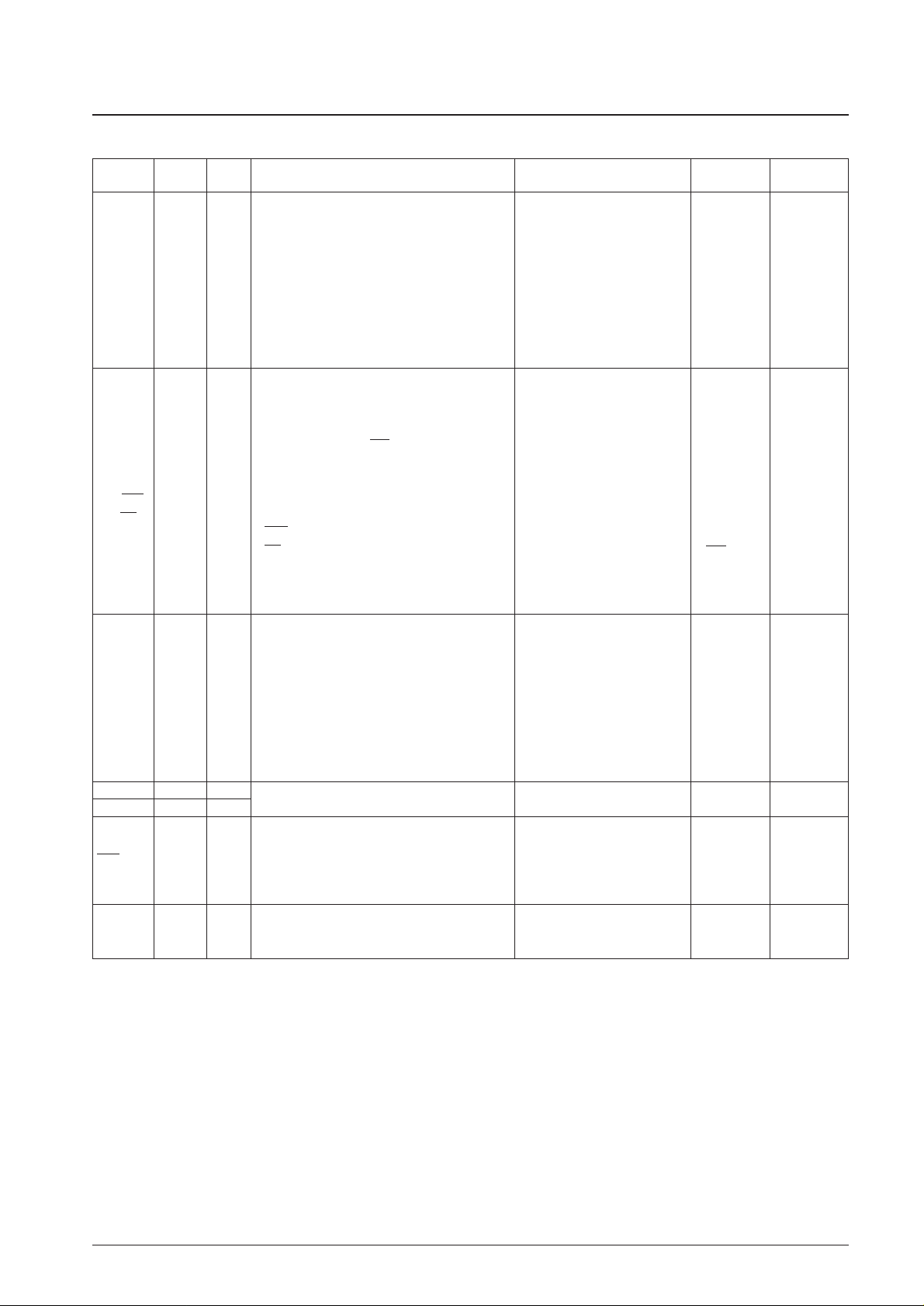
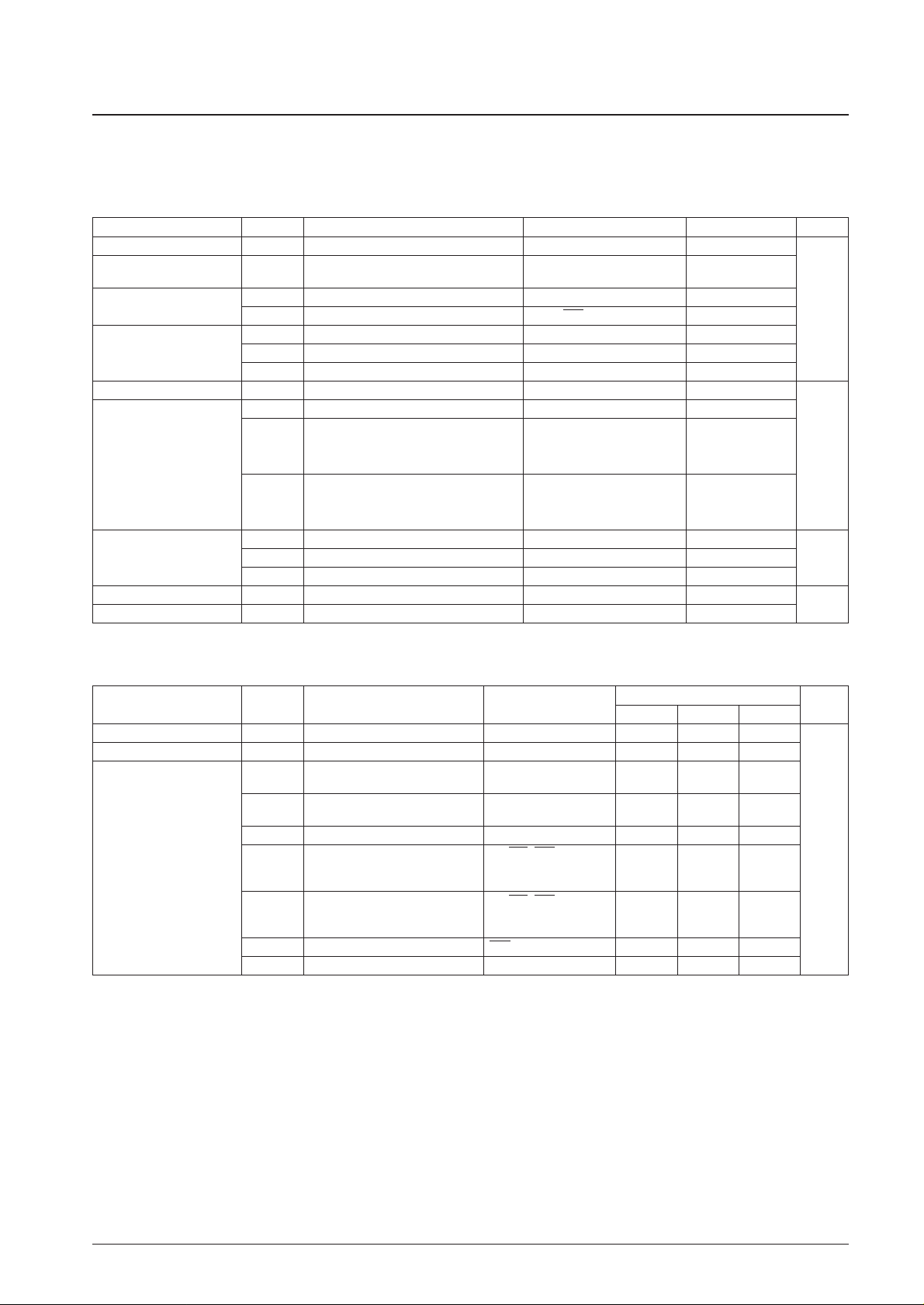
Differences between the LC651154N/1152N and the LC651104N/1102N.
The table below lists the points that require care when converting an existing product that uses the LC651104N/1102N to
use the LC651154N/1152N.
No. 6278-3/39
LC651154N, 651154F, 651154L, 651152N, 651152F, 651152L
Parameter LC651154N/1152N LC651104N/1102N
Pdmax (1) : DIP 310 mW 250 mW
Allowable power dissipation Pdmax (2) : MFP 220 mW 150 mW
Pdmax (3) : SSOP 160 mW (No corresponding package)
f
CFOSC
Oscillator frequency precision: within ±2%
[OSC1, OSC2]
Changes in the recommended oscillator
Oscillator frequency precision: within ±4%
constants (See table 1.)
800 kHz typ. (V
DD
= 3 to 6 V) 900 kHz typ. (VDD= 4 to 6 V)
Constants changed: Rext = 5.6 kΩ ±1 % Constants changed: Rext = 4.7 kΩ ±1 %
Frequency variability (sample to sample): Frequency variability (sample to sample):
587 to 1298 kHz 634 to 1278 kHz
400 kHz typ. (V
DD
= 3 to 6 V) 400 kHz typ. (VDD= 3 to 6 V)
Frequency variability (sample to sample): Frequency variability (sample to sample):
290 to 616 kHz 276 to 742 kHz
Pull-up resistors Ru [RES] 200 to 800 kΩ(500 kΩ typ.) 300 to 700 kΩ (500 kΩ typ.)
Serial clock input clock cycle time t
CKCY
(1) [ SCK] min. 2.0 µs min. 3.0 µs
A/D converter characteristics Operating voltage V
DD
= 3 to 6 V VDD= 4 to 6 V
AV+ = V
DD
Reference input current
200 to 800 µA (500 µA typ.) 75 to 300 µA (150 µA typ.)
AV– = V
SS
IRIF [AV+, AV–]
Watchdog timer
Cw = 0.047 ±5% µF
V
DD
= 3 to 6 V VDD= 4 to 6 V
Rw = 680 ±1% kΩ
RI = 100 ±1% Ω
Package
DIP30S-D, MFP30S
DIP30S-D, MFP30S
An SSOP30 version was added.
Differences between the LC651154F/1152F and the LC651104F/1102F.
The table below lists the points that require care when converting an existing product that uses the LC651104F/1102F to
use the LC651154F/1152F.
Parameter LC651154F/1152F LC651104F/1102F
Pdmax (1) : DIP 310 mW 250 mW
Allowable power dissipation Pdmax (2) : MFP 220 mW 150 mW
Pdmax (3) : SSOP 160 mW (No corresponding package)
Operating supply voltage V
DD
2.5 to 6 V 4 to 6 V
Specifications for V
DD
= 4 to 6 V
Low-level input voltage V
IL
(n) The specifications for VDD= 2.5 to 6 V Specifications for VDD= 4 to 6 V
were added.
Oscillator characteristics
Ceramic oscillator Oscillator frequency precision: within ±2 % Oscillator frequency precision: within ±4 %
Oscillator frequency
Pull-up resistors Ru [RES] 200 to 800 kΩ(500 kΩ typ.) 300 to 700 kΩ (500 kΩ typ.)
Operating voltage
AD speed 1/1 : V
DD
= 3.5 to 6 V AD speed 1/1 : VDD= 4.5 to 6 V
AD speed 1/2 : V
DD
= 3 to 6 V AD speed 1/2 : VDD= 4 to 6 V
Reference input current
200 to 800 µA (500 µA typ.) 75 to 300 µA (150 µA typ.)
IRIF [AV+, AV–]
Package
DIP30S-D, MFP30S
DIP30S-D, MFP30S
An SSOP30 version was added.
Oscillator characteristics
Ceramic oscillator
Oscillator frequency
2-pin RC oscillator
Oscillator frequency
f
MOSC
[OSC1, OSC2]
f
CFOSC
[OSC1, OSC2]
A/D converter characteristics
AV+ = V
DD
AV– = V
SS
Page 4
No. 6278-4/39
LC651154N, 651154F, 651154L, 651152N, 651152F, 651152L
Differences between the LC651154L/1152L and the LC651104L/1102L.
The table below lists the points that require care when converting an existing product that uses the LC651104L/1102L to
use the LC651154L/1152L.
Caution: Perform a full system evaluation and inspection after replacing the microcontroller.
Parameter LC651154L/1152L LC651104L/1102L
Pdmax (1) : DIP 310 mW 250 mW
Allowable power dissipation Pdmax (2) : MFP 220 mW 150 mW
Pdmax (3) : SSOP 160 mW (No corresponding package)
Operating supply voltage V
DD
2.2 to 6 V 2.5 to 6 V
Oscillator frequency precision: within ±2%
Changes in the recommended oscillator
Oscillator frequency precision: within ±4%
constants (See table 1.)
400 kHz typ. (V
DD
= 2.2 to 6 V) 400 kHz typ. (VDD= 2.5 to 6 V)
Frequency variability (sample to sample): Frequency variability (sample to sample):
290 to 841 kHz 276 to 742 kHz
Pull-up resistors Ru [RES] 200 to 800 kΩ(500 kΩ typ.) 300 to 700 kΩ (500 kΩ typ.)
Serial clock input clock cycle time t
CKCY
(1) [ SCK] min. 2.0 µs min. 6.0 µs
A/D converter characteristics Operating voltage V
DD
= 3 to 6 V VDD= 4 to 6 V
AV+ = V
DD
Reference input current
200 to 800 µA (500 µA typ.) 75 to 300 µA (150 µA typ.)
AV– = V
SS
IRIF [AV+, AV–]
Watchdog timer V
DD
= 2.2 to 6.0 V VDD= 2.5 to 6.0 V
Package
DIP30S-D, MFP30S
DIP30S-D, MFP30S
An SSOP30 version was added.
Oscillator characteristics
Ceramic oscillator
Oscillator frequency
2-pin RC oscillator
Oscillator frequency
f
CFOSC
[OSC1, OSC2]
f
MOSC
[OSC1, OSC2]
Page 5
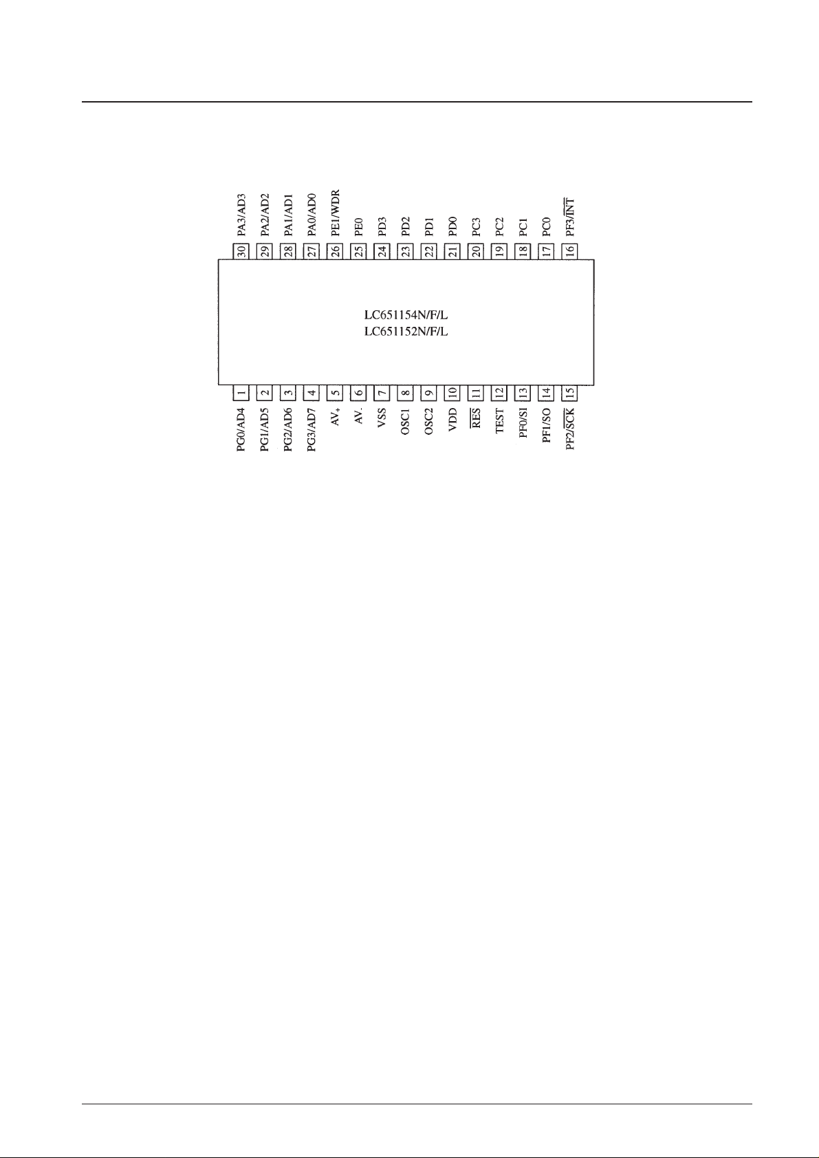
Pin Assignment
The pin assignment is the same for the DIP, MFP, and SSOP packages.
No. 6278-5/39
LC651154N, 651154F, 651154L, 651152N, 651152F, 651152L
Page 6
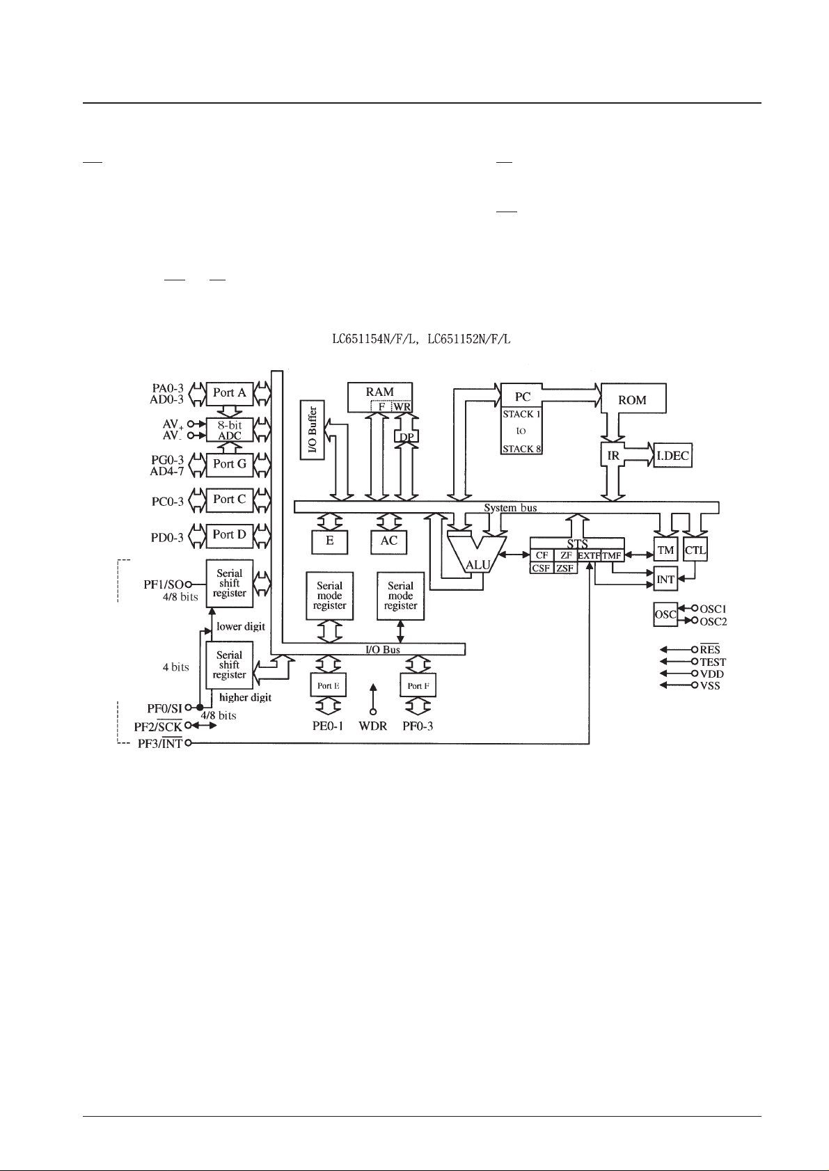
System Block Diagram
No. 6278-6/39
LC651154N, 651154F, 651154L, 651152N, 651152F, 651152L
Pin Functions
OSC1, OSC2: Connections for the oscillator capacitor and resistor or ceramic element TEST: IC testing.
RES: Reset INT: Interrupt request input
PA0 to PA3: Common I/O ports A0 to A3 SI: Serial input
PC0 to PC3: Common I/O ports C0 to C3 SO: Serial output
PD0 to PD3: Common I/O ports D0 to D3 SCK: Serial clock input output
PE0 to PE3: Common I/O ports E0 to E3 AD0 to AD7: A/D converter analog inputs
PF0 to PF3: Common I/O ports F0 to F3 AV
+
, AV–: A/D converter reference voltage inputs
PG0 to PG3: Common I/O ports G0 to G3 WDR: Watchdog timer reset input
Note: Pins SI, SO, SCK, and INT are shared function pins also used as PF0:3.
RAM: Data memory ROM: Program memory
F: Flag PC: Program counter
WR: Working register INT: Interrupt control
AC: Accumulator IR: Instruction register
ALU: Arithmetic and logic unit I.DEC: Instruction decoder
DP: Data pointer CF, CSF: Carry flag and carry save flag
E: E register ZF, ZSF: Zero flag and zero save flag
CTL: Control register EXTF: External interrupt request flag
OSC: Oscillator circuit TMF: Internal interrupt request flag
TM: Timer
STS: Status register
Shared with port F
Page 7

Development Support
The following are provided for development with the LC651154 and LC651152.
• User’s manual
See the “LC651104/1102 User’s Manual.”
• Development tools manual
See the “Four-Bit Microcontroller EVA86000 Development Tools Manual.”
• Software manual
“LC65/66 Series Software Manual”
• Development tools
— Program development (EVA86000 System)
— On-chip EPROM microcontroller <LC65E1104> for program evaluation
No. 6278-7/39
LC651154N, 651154F, 651154L, 651152N, 651152F, 651152L
Pin Functions
Symbol
Number
I/O Function Option At reset
Handling when
of pins unused
V
DD
V
SS
1
—
—
Power supply — — —
OSC1 1 Input
• Connection for the RC circuit or ceramic oscillator
element used for the system clock oscillator
• Leave OSC2 open when an external clock input is
used.
(1) Two-pin RC oscillator or
external clock
(2) Two-pin ceramic oscillator
(3) Divider option
1. No divider
2. Divide-by-3
3. Divide-by-4
——
• I/O port A0 to A3
Input in 4-bit units (IP instruction)
Output in 4-bit units (OP instruction)
Testing in 1-bit units (BP and BNP instructions)
Set and reset in 1-bit units (SPB and RPB
instructions)
• PA3 is used for standby mode control
• Application must assure that chattering does not
occur on the PA3 input during HALT instruction
execution.
• All four pins have shared functions
PA0/AD0 - A/D converter input AD0
PA1/AD1 - A/D converter input AD1
PA2/AD2 - A/D converter input AD2
PA3/AD3 - A/D converter input AD3
(1) Open-drain output
(2) Pull-up resistor
Options (1) and (2) can be
specified in bit units
High-level
output (The
output nchannel
transistors in
the off state.)
Select the
open-drain
output option
and connect
to V
SS
.
OSC2 1
Output
PA0 to
PA3/
AD0 to
AD3
4 I/O
• I/O port C0 to C3
The port functions are identical to those of PA0 to
PA3. (See note.)
• The output during a reset can be selected to be
either high or low as an option.
Note: This port has no standby mode control
function.
(1) Open-drain output
(2) Pull-up resistor
(3) High-level output during reset
(4) Low-level output during reset
• Options (1) and (2) can be
specified in bit units
• Options (3) and (4) are
specified 4 bits at a time
• High-level
output
• Low-level
output
(Depending
on option
selected.)
The same as
for PA0 to
PA3
PC0 to
PC3
4 I/O
• I/O port D0 to D3
The port functions and options are identical to
those of PC0 to PC3.
The same as PC0 to PC3
The same as
PC0 to PC3
The same as
for PA0 to
PA3
PD0 to
PD3
4 I/O
Continued on next page.
Page 8
No. 6278-8/39
LC651154N, 651154F, 651154L, 651152N, 651152F, 651152L
Continued from preceding page.
Symbol
Number
I/O Function Option At reset
Handling when
of pins unused
PE0-PE1/
WDR
2 I/O
• I/O port E0 to E1
Input in 4-bit units (IP instruction)
Output in 4-bit units (OP instruction)
Set and reset in 1-bit units (SPB and RPB
instructions)
Testing in 1-bit units (BP and BNP instructions)
• PE0 also has a continuous pulse (64·Tcyc) output
function.
• PE1 becomes the watchdog reset pin WDR when
selected for such as an option.
(1) Open-drain output
(2) Pull-up resistor
• Options (1) and (2) can be
specified in bit units
(3) Normal port PE1
(4) Watchdog reset WDR
• Either options (3) and (4)
may be specified.
High-level
output (The
output nchannel
transistors in
the off state.)
Identical to
those for PA0
to PA3
PF0/SI
PF1/SO
PF2/SCK
PF3/INT
4 I/O
• I/O port F0 to F3
The port functions and options are identical to
those of PE0 to PE1 (See note.)
• PF0 to PF3 have shared functions as the serial
interface pins and the INT input.
The function can be selected under program
control.
SI ... Serial input pin
SO ... Serial output pin
SCK ... Input and output of the serial clock signal
INT ... Interrupt request input
The serial I/O function can be switched between 4-
bit and 8-bit transfers under program control.
Note: There is no continuous pulse output function.
Identical to those for PA0 to PA3
Identical to
those for PA0
to PA3
The serial port
functions are
disabled.
The interrupt
source is set
to INT.
Identical to
those for PA0
to PA3
PG0-PG3/
AD4-AD7
4 I/O
• I/O port G0 to G3
The port functions and options are identical to
those of PE0 to PE1 (See note.)
Note: There is no continuous pulse output function.
• All four pins have shared functions.
PG0/AD4 - A/D converter input AD4
PG1/AD5 - A/D converter input AD5
PG2/AD6 - A/D converter input AD6
PG3/AD7 - A/D converter input AD7
Identical to those for PA0 to PA3
Identical to
those for PA0
to PA3
Identical to
those for PA0
to PA3
AV
+
1—
A/D converter reference voltage input — —
Connect to
V
SS
.
• System reset input
• Applications must provide an external capacitor for
the power-on reset.
• Apply a low level to this pin for 4 clock cycles to
effect and reset start.
———
AV
–
1—
RES 1 Input
• IC test pin
This pin must be connected to V
SS
during normal
operation.
——
This pin must
be connected
to V
SS
.
TEST 1 Input
Page 9
No. 6278-9/39
LC651154N, 651154F, 651154L, 651152N, 651152F, 651152L
Oscillator Circuit Options
Option Circuit Conditions and other notes
Ceramic
oscillator element
Divider Circuit Options
Option Circuit Conditions and other notes
• This option can be used with any of the three oscillator
options.
• The oscillator frequency or external clock frequency must
not exceed 1444 kHz. (LC651154N, LC651152N)
• The oscillator frequency or external clock frequency must
not exceed 4330 kHz. (LC651154F, LC651152F)
• The oscillator frequency or external clock frequency must
not exceed 1040 kHz. (LC651154L, LC651152L)
• This option can only be used with the external clock and the
ceramic oscillator options.
• The oscillator frequency or external clock frequency must
not exceed 4330 kHz.
• This option can only be used with the external clock and the
ceramic oscillator options.
• The oscillator frequency or external clock frequency must
not exceed 4330 kHz.
Oscillator circuit
Caution: The following tables summarize the oscillator and divider circuit options. Use care when selecting these options.
Timing
generator
Oscillator circuit
Oscillator circuit
Timing
generator
Timing
generator
External clock
Two-pin RC oscillator
Ceramic oscillator
The OSC2 pin must be left open.
No divider
Built-in divide-by-three circuit
Built-in divide-by-four circuit
Divide-by-3
Divide-by-4
Page 10
No. 6278-10/39
LC651154N, 651154F, 651154L, 651152N, 651152F, 651152L
LC651154N, LC651152N
Oscillator Options
Circuit type Frequency
Divider option
VDDrange Notes
(cycle time)
400 kHz 1/1 (10 µs) 3 to 6 V
Cannot be used with the divide-by-three
and divide-by-four options.
1/1 (5 µs) 3 to 6 V
800 kHz 1/3 (15 µs) 3 to 6 V
1/4 (20 µs) 3 to 6 V
1/1 (4 µs) 3 to 6 V
1 MHz 1/3 (12 µs) 3 to 6 V
1/4 (16 µs) 3 to 6 V
4 MHz
1/3 (3 µs) 3 to 6 V
Cannot be used with the no divider circuit
1/4 (4 µs) 3 to 6 V
option.
200 k to 1444 kHz 1/1 (20 to 2.77 µs) 3 to 6 V
600 k to 4330 kHz 1/3 (20 to 2.77 µs) 3 to 6 V
800 k to 4330 kHz 1/4 (20 to 3.70 µs) 3 to 6 V
Use the no divider circuit option and the 3 to 6 V
recommended circuit constants. If using other circuit
constants is unavoidable, the application must use a
frequency identical to the external clock and observe
the V
DD
range specification.
External clock used with the ceramic oscillator option External clock drive is not possible. To use external clock drive, select the 2-pin RC oscillator option.
LC651154F, LC651152F
Circuit type Frequency
Divider option
VDDrange Notes
(cycle time)
Ceramic oscillator 4 MHz 1/1 (1 µs) 2.5 to 6 V
External clock used with the 2-pin RC oscillator circuit 200 k to 4330 kHz 1/1 (20 to 0.92 µs) 2.5 to 6 V
External clock used with the ceramic oscillator option External clock drive is not possible. To use external clock drive, select the 2-pin RC oscillator option.
Ceramic oscillator
External clock used with the 2-pin RC oscillator circuit
Two-pin RC
Page 11
No. 6278-11/39
LC651154N, 651154F, 651154L, 651152N, 651152F, 651152L
LC651154L, LC651152L
Circuit type Frequency
Divider option
VDDrange Notes
(cycle time)
400 kHz 1/1 (10 µs) 2.2 to 6 V
Cannot be used with the divide-by-three
and divide-by-four options.
1/1 (5 µs) 2.2 to 6 V
800 kHz 1/3 (15 µs) 2.2 to 6 V
1/4 (20 µs) 2.2 to 6 V
1/1 (4 µs) 2.2 to 6 V
1 MHz 1/3 (12 µs) 2.2 to 6 V
1/4 (16 µs) 2.2 to 6 V
Cannot be used with either the no divider
4 MHz 1/4 (4 µs) 2.2 to 6 V circuit option or the divide-by-three circuit
option.
200 k to 1040 kHz 1/1 (20 to 3.84 µs) 2.2 to 6 V
600 k to 3120 kHz 1/3 (20 to 3.84 µs) 2.2 to 6 V
800 k to 4160 kHz 1/4 (20 to 3.84 µs) 2.2 to 6 V
Use the no divider circuit option and the 2.2 to 6 V
recommended circuit constants. If using other circuit
constants is unavoidable, the application must use a
frequency identical to the external clock and observe
the V
DD
range specification.
External clock used with the ceramic oscillator option External clock drive is not possible. To use external clock drive, select the 2-pin RC oscillator option.
Port C and D Output Level During Reset Option
The output level during a reset can be selected from the two options below in 4-bit units for the C and D ports.
Port Output Type Option
The following two options may be selected for the I/O ports individually (bit units).
Watchdog Reset Option
This option allows the PE1/WDR pin to be selected either to be used as the normal port PE1 or to be used as the
watchdog reset pin WDR.
Option Conditions and other notes
High-level output during reset Ports C and D in 4-bit units
Low-level output during reset Ports C and D in 4-bit units
Option Circuit Applicable ports
Ceramic oscillator
External clock used with the 2-pin RC oscillator circuit
Two-pin RC
1. Open-drain output
2. Built-in pull-up resistor
Ports A, C, D, E, F, and G
Page 12
LC651154N, 651152N
No. 6278-12/39
LC651154N, 651154F, 651154L, 651152N, 651152F, 651152L
Parameter Symbol Conditions Applicable pins and notes Ratings Unit
Maximum supply voltage V
DD
max V
DD
–0.3 to +7.0
Output voltage V
O
OSC2
Allowed up to the
generated voltage.
Input voltage
V
I
(1) OSC1 *
1
–0.3 to VDD+ 0.3
V
V
I
(2) TEST, RES, AV+, AV
–
–0.3 to VDD+ 0.3
V
IO
(1) PC0 to 3, PD0 to 3, PE0, 1, PF0 to 3 Open-drain specification ports –0.3 to +15
I/O voltage V
IO
(2) PC0 to 3, PD0 to 3, PE0, 1, PF0 to 3
Pull-up resistor specification ports
–0.3 to VDD+ 0.3
V
IO
(3) PC0 to 3, PG0 to 3 –0.3 to VDD+ 0.3
Peak output current I
OP
I/O ports –2 to +20
I
OA
Per single pin, averaged over 100 ms I/O ports –2 to +20
The total current for PC0 to PC3,
PC0 to 3
∑I
OA
(1)
PD0 to PD3, and PE0 to PE1 *
2
PD0 to 3 –15 to +100
mA
Average output current PE0 to 1
The total current for PF0 to PF3,
PF0 to 3
∑I
OA
(2)
PG0 to PG3, and PA0 to PA3 (See note 2.) *
2
PG0 to 3 –15 to +100
PA0 to 3
Pd max (1) Ta = –40 to +85°C (DIP package) 310
Allowable power dissipation Pd max (2) Ta = –40 to +85°C (MFP package) 220 mW
Pd max (3) Ta = –40 to +85°C (SSOP package) 160
Operating temperature Topr –40 to +85
°C
Storage temperature Tstg –55 to +125
Absolute Maximum Ratings at Ta = 25°C, VSS= 0 V
Parameter Symbol Conditions Applicable pins and notes
Ratings
Unit
min typ max
Operating supply voltage V
DD
V
DD
3.0 6.0
Standby supply voltage V
ST
RAM and register values retained*3V
DD
1.8 6.0
V
IH
(1) Output n-channel transistors off
Ports C, D, E, and F with
0.7 V
DD
13.5
open-drain specifications
VIH(2) Output n-channel transistors off
Ports C, D, E, and F with
0.7 V
DD
V
DD
pull-up resistor specifications
VIH(3) Output n-channel transistors off Port A, G 0.7 V
DD
V
DD
V
The INT, SCK, and SI
High-level input voltage VIH(4) Output n-channel transistors off pins with open-drain 0.8 V
DD
13.5
specifications
The INT, SCK, and SI
V
IH
(5) Output n-channel transistors off pins with pull-up resistor 0.8 V
DD
V
DD
specifications
V
IH
(6) VDD= 1.8 to 6.0 V RES 0.8 V
DD
V
DD
VIH(7) External clock specifications OSC1 0.8 V
DD
V
DD
Allowable Operating Ranges at Ta = –40 to +85°C, VSS= 0 V, VDD= 3.0 to 6.0 V (Unless otherwise specified.)
Continued on next page.
Page 13

No. 6278-13/39
LC651154N, 651154F, 651154L, 651152N, 651152F, 651152L
Parameter Symbol Conditions
Applicable pins
Ratings
Unit
and notes min typ max
V
IL
(1)
Output n-channel transistors off
VDD= 4 to 6 V Port V
SS
0.3 V
DD
VIL(2)
Output n-channel transistors off
VDD= 3 to 6 V Port V
SS
0.25 V
DD
VIL(3)
Output n-channel transistors off
VDD= 4 to 6 V INT, SCK, SI V
SS
0.25 V
DD
VIL(4)
Output n-channel transistors off
VDD= 3 to 6 V INT, SCK, SI V
SS
0.2 V
DD
Low-level input voltage
V
IL
(5) External clock specifications VDD= 4 to 6 V OSC1 V
SS
0.25 V
DD
V
V
IL
(6) External clock specifications VDD= 3 to 6 V OSC1 V
SS
0.2 V
DD
VIL(7) VDD= 4 to 6 V TEST V
SS
0.3 V
DD
VIL(8) VDD= 3 to 6 V TEST V
SS
0.25 V
DD
VIL(9) VDD= 4 to 6 V RES V
SS
0.25 V
DD
VIL(10) VDD= 3 to 6 V RES V
SS
0.2 V
DD
The clock may have a
frequency up to 4.33 MHz
Operating frequency
fop (Tcyc)
when either the divide-by-
V
DD
= 3 to 6 V
200 1444
kHz (µs)
(cycle time) three or divide-by-four (20) (2.77)
internal divider circuit option
is used.
External clock conditions Figure 1.
Frequency text V
DD
= 3 to 6 V OSC1 200 4330 kHz
Pulse width textH, textL V
DD
= 3 to 6 V OSC1 69
ns
Rise and fall times textR, textF VDD= 3 to 6 V OSC1 50
Recommended oscillator
circuit constants Cext
Figure 2 V
DD
= 3 to 6 V OSC1, OSC2
270 ±5% pF
Rext 12 ±1% kΩ
Two-pin RC oscillator
Cext
Figure 2 V
DD
= 3 to 6 V OSC1, OSC2
270 ±5% pF
Rext 5.6 ±1% kΩ
Ceramic oscillator *
4
Figure 3
See table 1.
Continued from preceding page.
Either the divide-bythree or divide-by-four
internal divider circuit
must be used if the
clock frequency
exceeds 1.444 MHz.
Page 14

No. 6278-14/39
LC651154N, 651154F, 651154L, 651152N, 651152F, 651152L
Parameter Symbol Conditions Applicable pins and notes
Ratings
Unit
min typ max
• Output n-channel transistors off
I
IH
(1)
(Including the n-channel transistor
5.0
off leakage current.)
• V
IN
= 13.5 V
High-level input current
• Output n-channel transistors off
I
IH
(2)
(Including the n-channel transistor Ports A and G with the
1.0
µA
off leakage current.) open-drain specifications
• V
IN
= V
DD
IIH(3)
When an external clock is used,
OSC1 1.0
V
IN
= V
DD
IIL(1)
• Output n-channel transistors off Ports with the open-drain
–1.0
• V
IN
= V
SS
specifications
I
IL
(2)
• Output n-channel transistors off Ports with the pull-up
–1.3 –0.35 mA
Low-level input current • V
IN
= V
SS
resistor specifications
I
IL
(3) VIN= V
SS
RES –45 –10
I
IL
(4)
When an external clock is used, OSC1 –1.0
µA
V
IN
= V
SS
VOH(1)
• I
OH
= –50 µA Ports with the pull-up
V
DD
– 1.2
High-level output voltage
• V
DD
= 4.0 to 6.0 V resistor specifications
V
OH
(2) IOH= –10 µA
Ports with the pull-up
VDD– 0.5
resistor specifications
VOL(1)
• I
OL
= 10 mA
Port 1.5
Low-level output voltage
• V
DD
= 4.0 to 6.0 V
V
OL
(2)
When I
OL
= 1 mA and the IOLfor
Port 0.5
V
each port is 1 mA or less.
Hysteresis voltage V
HIS
0.1 V
DD
High-level threshold
V
tH
0.4 V
DD
0.8 V
DD
voltage
Low-level threshold
V
tL
0.2 V
DD
0.6 V
DD
voltage
Current drain *
6
• Operating, with the output
IDDOP (1)
n-channel transistors off
V
DD
1.5 4
Two-pin RC oscillator • With the ports at V
DD
• Figure 2, fosc = 800 kHz (typical)
Ceramic oscillator IDDOP (2) •
Figure 3, 4 MHz, divide-by-three circuit used
V
DD
1.5 5
IDDOP (3) •
Figure 3, 4 MHz, divide-by-four circuit used
V
DD
1.5 4
IDDOP (4) • Figure 3, 400 kHz V
DD
1.0 2.5 mA
IDDOP (5) • Figure 3, 800 kHz V
DD
1.5 4
• 200 kHz to 1444 kHz, no divider
circuit
External clock IDDOP (6)
• 600 kHz to 4330 kHz, divide-by-
V
DD
1.5 5
three circuit used
• 800 kHz to 4330 kHz, divide-by-
four circuit used
Output n-channel transistors off, V
DD
0.05 10
Standby mode IDDst
V
DD
= 6 V µA
Ports at V
DD
, VDD= 3 V V
DD
0.025 5
Electrical Characteristics at Ta = –40 to +85°C, VSS= 0 V, VDD= 3.0 to 6.0 V (Unless otherwise specified.)
Schmitt characteristics
Continued on next page.
RES, INT, SCK, SI, and
OSC1 with Schmitt
specifications*
5
Ports C, D, E and F with
the open-drain
specifications
Page 15

No. 6278-15/39
LC651154N, 651154F, 651154L, 651152N, 651152F, 651152L
Parameter Symbol Conditions Applicable pins and notes
Ratings
Unit
min typ max
Oscillator characteristics • Figure 3, fo = 400 kHz OSC1, OSC2 392 400 408
• Figure 3, fo = 800 kHz OSC1, OSC2 784 800 816
Ceramic oscillator
f
CFOSC
*
7
• Figure 3, fo = 1 MHz OSC1, OSC2 980 1000 1020
kHz
Oscillator frequency • Figure 3, fo = 4 MHz, with the OSC1, OSC2 3920 4000 4080
divide-by-three or divide-by-four
circuit used.
Oscillator stabilization time • Figure 4, fo = 400 kHz 10
(note 8)
t
CFS
• Figure 4, fo = 800 kHz, 1 MHz, or 10
ms
4 MHz, with the divide-by-three or
divide-by-four circuit used.
Two-pin RC oscillator • Figure 2, Cext = 270 pF ±5%
OSC1, OSC2 587 800 1298
Oscillator frequency
f
MOSC
• Figure 2, Rext = 5.6 kΩ ±1%
kHz
• Figure 2, Cext = 270 pF ±5%
OSC1, OSC2 290 400 818
• Figure 2, Rext = 12 kΩ ±1%
Pull-up resistor
RPP
• Output n-channel transistors off Pull-up resistor
814 30
I/O ports • V
IN
= VSS, VDD= 5 V specification ports
kΩ
RES Ru V
IN
= VSS, VDD= 5 V RES 200 500 800
External reset characteristics
t
RST
See figure 5.
Reset time
• f = 1 MHz
Pin capacitances Cp • With all pins other than the pin 10 pF
being tested at V
IN
= VSS.
Serial clock
Input clock cycle time
t
CKCY
(1) Figure 6 SCK 2.0
Output clock cycle time t
CKCY
(2) Figure 6 SCK
64 × TCYC*
9
Input clock low-level pulse
t
CKL
(1) Figure 6 SCK 1.0
width
Output clock low-level pulse
t
CKL
(2) Figure 6 SCK
32 × TCYC
width
Input clock high-level pulse
t
CKH
(1) Figure 6 SCK 1.0
width
Output clock high-level
t
CKH
(2) Figure 6 SCK
32 × TCYC
pulse width
Serial input
Data setup time t
ICK
SI 0.4
Data hold time t
CKI
SI 0.4
Serial output • Stipulated with respect to the
falling edge of SCK.
• With an external resistor of 1 kΩ
Output delay time t
CKO
and an external capacitor of 50 pF SO 0.6
on only the n-channel open-drain
pins.
• Figure 6
Continued from preceding page.
Continued on next page.
• Stipulated with respect to the
rising edge of SCK.
• Figure 6
µs
Page 16

No. 6278-16/39
LC651154N, 651154F, 651154L, 651152N, 651152F, 651152L
Continued from preceding page.
Parameter Symbol Conditions
Applicable pins
Ratings
Unit
and notes min typ max
Pulse output function
t
PCY
PE0
64 × T
CYC
Period
High-level pulse width t
PH
PE0
32 × T
CYC
±10%
µs
Low-level pulse width t
PL
PE0
32 × T
CYC
±10%
Resolution 8 bit
Absolute precision
AV
+
= V
DD
±1 ±2 LSB
AV
–
= V
SS
When the A/D converter 72 312
speed is normal (1:1), (T
CYC
= (T
CYC
=
namely 26 × T
CYC
2.77 µs) 12 µs)
Conversion time TCAD
When the A/D converter 141 612
µs
speed is one half (1:2), (T
CYC
= (T
CYC
=
namely 51 × T
CYC
2.77 µs) 12 µs)
Input reference voltage
AV
+
AV
+
AV
–
V
DD
V
AV
–
AV
–
V
SS
AV
+
Input reference current
IRIF AV
+
= VDD, AV–= V
SS
AV+, AV
–
200 500 800 µA
range
Analog input voltage
V
AIN
AD0 to AD7 AV
–
AV+V
range
Including the output off AD0 to AD7 1
leakage current. (The I/O
V
AIN
= V
DD
shared
Analog port input current I
AIN
function ports µA
V
AIN
= V
SS
have open-
–1
drain
specifications.)
Cw
When PE1 has the
WDR 0.1 ±5% µF
open-drain specifications.
Recommended
Rw
When PE1 has the
WDR 680 ±1% kΩ
constants*
10
open-drain specifications.
RI
When PE1 has the
WDR 100 ±1% Ω
open-drain specifications.
Clear time (discharge) t
WCT
Figure 8 WDR 100 µs
Clear period (charge) t
WCCY
Figure 8 WDR 36 ms
Cw
When PE1 has the
WDR 0.047 ±5% µF
open-drain specifications.
Recommended
Rw
When PE1 has the
WDR 680 ±1% kΩ
constants*
10
open-drain specifications.
RI
When PE1 has the
WDR 100 ±1% Ω
open-drain specifications.
Clear time (discharge) t
WCT
Figure 8 WDR 40 µs
Clear period (charge) t
WCCY
Figure 8 WDR 18 ms
A/D converter characteristicsWatchdog timer
Notes:1. Allowed up to the amplitude generated when the oscillator shown in figure 3 is used with the recommended circuit constants and driven by the IC.
2. The average over a 100 ms period.
3. The operating V
DD
supply voltage must be maintained from the point the HALT instruction is executed until the IC has fully entered the standby
state. Applications must also assure that no chattering occurs on the PA3 pin during the HALT instruction execution cycle.
4. Recommended circuit constants that have been verified to oscillate stably according to the oscillator element manufacturer using the Sanyostipulated oscillator characteristics evaluation board.
5. The OSC1 pin will have Schmitt characteristics when external clock oscillator is selected with the two-pin RC oscillator option.
6. These are the results of testing using our (Sanyo’s) characteristics evaluation board with the recommended circuit constants used as external
components. The current flowing in the IC’s output transistors and transistors that have pull-up resistors is not included.
7. f
CFOSC
is the frequency when the recommended circuit constants from table 1 are used as external components.
8. Indicates the time required to achieve stable oscillation from the point V
DD
rises above the lower limit of the operating voltage range.
9. TCYC = 4 × the system clock period
10. If the application could be used in an environment in which condensation is possible, extra care with respect to the leakage between PE1 and
adjacent pins and leakage associated with external resistors and capacitor is required during design.
VDD= 3 to 6 V
V
DD
= 3 to 6 V
V
DD
= 3 to 6 V
• Figure 7
• T
CYC
= 4 × system clock
period
• With an external resistor of
1 kΩ and an external
capacitor of 50 pF on only
the n-channel open-drain
pins.
Page 17

No. 6278-17/39
LC651154N, 651154F, 651154L, 651152N, 651152F, 651152L
External clock
Figure 1 External Clock Input Waveform
Figure 2 Two-Pin RC Oscillator Circuit Figure 3 Ceramic Oscillator Circuit
open
Ceramic oscillator
element
Page 18

No. 6278-18/39
LC651154N, 651154F, 651154L, 651152N, 651152F, 651152L
Stable oscillation
Figure 4 Oscillation Stabilization Time
Figure 5 Reset Circuit
Note: If the power supply rise time is zero, the reset time when CRES = 0.1 µF
will be between 10 and 100 ms.
If the power supply rise time is long, increase the value of CRES so that
the reset time is at least 10 ms.
Table 1 Recommended Ceramic Oscillator Circuit Constants
4 MHz (Murata Mfg. Co., Ltd.) C1 33 pF ±10%
CSA4.00MG C2 33 pF ±10%
CST4.00MGW (Internal capacitor) R 0 Ω
4 MHz (Kyocera Corporation) C1 33 pF ±10%
KBR4.0MSA C2 33 pF ±10%
KBR4.0MKS (Internal capacitor) R 0 Ω
1 MHz (Murata Mfg. Co., Ltd.) C1 100 pF ±10%
CSB1000J C2 100 pF ±10%
R 3.3 kΩ
800 kHz (Murata Mfg. Co., Ltd.) C1 100 pF ±10%
CSB800J C2 100 pF ±10%
R 3.3 kΩ
400 kHz (Murata Mfg. Co., Ltd.) C1 220 pF ±10%
CSB400P C2 220 pF ±10%
R 3.3 kΩ
Oscillation
stabilization
time t
CFS
Lower limit for the operating supply voltage
Page 19

No. 6278-19/39
LC651154N, 651154F, 651154L, 651152N, 651152F, 651152L
Input data
Figure 6 Serial I/O Timing
The load conditions are the same
as those in figure 5.
Figure 7 Port PE0 Pulse Output Timing
t
WCCY
: The charge time due to the time constant of the circuit consisting of
the external components Cw, Rw, and Rl.
t
WCT
: The discharge time due to software processing.
Figure 8 Watchdog Timer Waveform
Output data
Load circuit
Page 20

RC Oscillator Characteristics for the LC651154N and LC651152N
Figure 9 shows the RC oscillator characteristics for the LC651154N and LC651152N.
However, the sample-to-sample variation in the LC651154N and LC651152N RC oscillator frequency described below
does occur.
1) When:
VDD= 3.0 to 6.0 V, Ta = –40 to +85°C
External constants: Cext = 270 pF
Rext = 12.0 kΩ
f
MOSC
will be:
290 kHz ≤ f
MOSC
≤ 818 kHz
2) When:
VDD= 3.0 to 6.0 V, Ta = –40 to +85°C
External constants: Cext = 270 pF
Rext = 5.6 kΩ
f
MOSC
will be:
587 kHz ≤ f
MOSC
≤ 1298 kHz
Therefore, only the above circuit constants are recommended.
If use of circuit constants other than the above is unavoidable, they must be in the following ranges.
Cext = 150 to 390 pF
Rext = 3 to 20 kΩ
(See figure 9.)
Notes • The oscillator frequency must be in the range 350 to 850 kHz when VDD= 5.0 V and Ta = 25°C.
• Applications must be designed to have adequate margins so that the oscillator frequency falls in the operating
clock frequency range (see the oscillator divider option table) for the voltage range VDD= 3.0 to 6.0 V and for
the temperature range Ta = –40 to +85°C.
No. 6278-20/39
LC651154N, 651154F, 651154L, 651152N, 651152F, 651152L
These characteristics curves are for
reference purposes only and are not
guaranteed.
Figure 9 RC Oscillator Frequency Data (Representative Values)
Page 21

No. 6278-21/39
LC651154N, 651154F, 651154L, 651152N, 651152F, 651152L
LC651154F, 651152F
Absolute Maximum Ratings at Ta = 25°C, VSS= 0 V
Parameter Symbol Conditions Applicable pins and notes Ratings Unit
Maximum supply voltage V
DD
max V
DD
–0.3 to +7.0
Output voltage V
O
OSC2
Allowed up to the
generated voltage.
Input voltage
V
I
(1) OSC1 *
1
–0.3 to VDD+ 0.3
V
V
I
(2) TEST, RES, AV+, AV
–
–0.3 to VDD+ 0.3
V
IO
(1)
PC0 to PC3, PD0 to PD3, PE0, 1, PF0 to PF3
Open-drain specification ports –0.3 to +15
I/O voltage V
IO
(2)
PC0 to PC3, PD0 to PD3, PE0, 1, PF0 to PF3
Pull-up resistor specification ports
–0.3 to VDD+ 0.3
V
IO
(3) PA0 to PA3, PG0 to PG3 –0.3 to VDD+ 0.3
Peak output current I
OP
I/O ports –2 to +20
I
OA
Per single pin, averaged over 100 ms I/O ports –2 to +20
The total current for PC0 to PC3,
PC0 to PC3
∑I
OA
(1)
PD0 to PD3, and PE0 and PE1 *
2
PD0 to PD3 –15 to +100
mA
Average output current PE0 and PE1
The total current for PF0 to PF3, PG0 to PG3,
PF0 to PF3
∑I
OA
(2)
and PA0 to PA3 (See note 2.) *
2
PG0 to PG3 –15 to +100
PA0 to PA3
Pd max (1) Ta = –40 to +85°C (DIP package) 310
Allowable power dissipation Pd max (2) Ta = –40 to +85°C (MFP package) 220 mW
Pd max (3) Ta = –40 to +85°C (SSOP package) 160
Operating temperature Topr –40 to +85
°C
Storage temperature Tstg –55 to +125
Parameter Symbol Conditions Applicable pins and notes
Ratings
Unit
min typ max
Operating supply voltage V
DD
V
DD
2.5 6.0
Standby supply voltage V
ST
RAM and register values retained*3V
DD
1.8 6.0
V
IH
(1) Output n-channel transistors off
Ports C, D, E, and F with
0.7 V
DD
13.5
open-drain specifications
VIH(2) Output n-channel transistors off
Ports C, D, E, and F with
0.7 V
DD
V
DD
pull-up resistor specifications
VIH(3) Output n-channel transistors off Port A, G 0.7 V
DD
V
DD
V
The INT, SCK, and SI
High-level input voltage VIH(4) Output n-channel transistors off pins with open-drain 0.8 V
DD
13.5
specifications
The INT, SCK, and SI
V
IH
(5) Output n-channel transistors off pins with pull-up resistor 0.8 V
DD
V
DD
specifications
V
IH
(6) VDD= 1.8 to 6.0 V RES 0.8 V
DD
V
DD
VIH(7) External clock specifications OSC1 0.8 V
DD
V
DD
Allowable Operating Ranges at Ta = –40 to +85°C, VSS= 0 V, VDD= 2.5 to 6.0 V (Unless otherwise specified.)
Continued on next page.
Page 22

No. 6278-22/39
LC651154N, 651154F, 651154L, 651152N, 651152F, 651152L
Parameter Symbol Conditions
Applicable pins
Ratings
Unit
and notes min typ max
V
IL
(1)
Output n-channel transistors off
VDD= 4 to 6 V Port V
SS
0.3 V
DD
VIL(2)
Output n-channel transistors off
VDD= 2.5 to 6 V Port V
SS
0.2 V
DD
VIL(3)
Output n-channel transistors off
VDD= 4 to 6 V INT, SCK, SI V
SS
0.25 V
DD
VIL(4)
Output n-channel transistors off
VDD= 2.5 to 6 V INT, SCK, SI V
SS
0.15 V
DD
Low-level input voltage
V
IL
(5) External clock specifications VDD= 4 to 6 V OSC1 V
SS
0.25 V
DD
V
V
IL
(6) External clock specifications VDD= 2.5 to 6 V OSC1 V
SS
0.15 V
DD
VIL(7) VDD= 4 to 6 V TEST V
SS
0.3 V
DD
VIL(8) VDD= 2.5 to 6 V TEST V
SS
0.2 V
DD
VIL(9) VDD= 4 to 6 V RES V
SS
0.25 V
DD
VIL(10) VDD= 2.5 to 6 V RES V
SS
0.15 V
DD
Operating frequency
fop (Tcyc)
200 4330
kHz (µs)
(cycle time) (20) (0.92)
External clock conditions
Frequency text OSC1 200 4330 kHz
Pulse width textH, textL Figure 1. OSC1 69 ns
Rise and fall times textR, textF OSC1 50 ns
Recommended oscillator
circuit constants Figure 2
See table 1.
Ceramic oscillator *
4
Parameter Symbol Conditions Applicable pins and notes
Ratings
Unit
min typ max
• Output n-channel transistors off
Ports C, D, E and F with
I
IH
(1)
(Including the n-channel transistor
the open-drain 5.0
off leakage current.)
specifications
• V
IN
= 13.5 V
High-level input current
• Output n-channel transistors off
I
IH
(2)
(Including the n-channel transistor Ports A and G with the
1.0
µA
off leakage current.) open-drain specifications
• V
IN
= V
DD
IIH(3) When an external clock is used,
OSC1 1.0
V
IN
= V
DD
IIL(1)
• Output n-channel transistors off Ports with the open-drain
–1.0
• V
IN
= V
SS
specifications
I
IL
(2)
• Output n-channel transistors off Ports with the pull-up
–1.3 –0.35 mA
Low-level input current • V
IN
= V
SS
resistor specifications
I
IL
(3) VIN= V
SS
RES –45 –10
I
IL
(4)
When an external clock is used,
OSC1 –1.0
µA
V
IN
= V
SS
VOH(1)
• I
OH
= –50 µA Ports with the pull-up
V
DD
– 1.2
High-level output voltage
• V
DD
= 4.0 to 6.0 V resistor specifications
V
OH
(2) IOH= –10 µA
Ports with the pull-up
VDD– 0.5
resistor specifications
VOL(1)
• I
OL
= 10 mA
Port 1.5
Low-level output voltage
• V
DD
= 4.0 to 6.0 V
V
OL
(2)
When I
OL
= 1 mA and the IOLfor
Port 0.5
V
each port is 1 mA or less.
Hysteresis voltage V
HIS
0.1 V
DD
High-level threshold
V
tH
0.4 V
DD
0.8 V
DD
voltage
Low-level threshold
V
tL
0.25 V
DD
0.6 V
DD
voltage
Electrical Characteristics at Ta = –40 to +85°C, VSS= 0 V, VDD= 2.5 to 6.0 V (Unless otherwise specified.)
Schmitt characteristics
Continued on next page.
Continued from preceding page.
RES, INT, SCK, SI, and
OSC1 with Schmitt
specifications*
5
Page 23

No. 6278-23/39
LC651154N, 651154F, 651154L, 651152N, 651152F, 651152L
Parameter Symbol Conditions Applicable pins and notes
Ratings
Unit
min typ max
Current drain*
6
IDDOP (1) • Figure 2, 4 MHz V
DD
26
• 200 kHz to 4330 kHz
mA
Ceramic oscillator • Operating, with the output
IDDOP (2) n-channel transistors off and the V
DD
26
ports at V
DD
.
• Output n-channel transistors off
V
DD
0.05 10
µA
Standby mode IDDst VDD= 6 V
• Ports at V
DD
, VDD= 2.5 V
V
DD
0.025 5
Oscillator characteristics
Ceramic oscillator
f
CFOSC
*7• Figure 2, fo = 4 MHz OSC1, OSC2 3920 4000 4080 kHz
Oscillator frequency*8t
CFS
• Figure 3, fo = 4 MHz 10 ms
Pull-up resistor
RPP
• Output n-channel transistors off Pull-up resistor
814 30
kΩ
I/O ports • VIN= VSS, VDD= 5 V specification ports
RES Ru V
IN
= VSS, VDD= 5 V RES 200 500 800
External reset characteristics
t
RST
See figure 4.
Reset time
• f = 1 MHz
Pin capacitances Cp • With all pins other than the pin 10 pF
being tested at V
IN
= VSS.
Serial clock
Input clock cycle time
t
CKCY
(1) Figure 5 SCK 2.0
Output clock cycle time t
CKCY
(2) Figure 5 SCK
64 × T
CYC
*
9
Input clock low-level pulse
t
CKL
(1) Figure 5 SCK 0.6
width
Output clock low-level pulse
t
CKL
(2) Figure 5 SCK
32 × T
CYC
width
Input clock high-level pulse
t
CKH
(1) Figure 5 SCK 0.6
width
Output clock high-level
t
CKH
(2) Figure 5 SCK
32 × T
CYC
pulse width
Serial input
Data setup time t
ICK
• Stipulated with respect to the SI 0.2
rising edge of SCK. µs
• Figure 5
Data hold time t
CKI
SI 0.2
Serial output • Stipulated with respect to the
falling edge of SCK.
• With an external resistor of 1 kΩ
SO 0.4
Output delay time t
CKO
and an external capacitor of 50 pF
on only the n-channel open-drain
pins.
• Figure 5
Pulse output function
Period t
PCY
• Figure 6 PE0
64 × T
CYC
• T
CYC
= 4 × system clock
period
High-level pulse width t
PH
• With an external resistor of PE0
32 × T
CYC
1 kΩ and an external ±10%
capacitor of 50 pF on only
Low-level pulse width t
PL
the n-channel open-drain
PE0
32 × T
CYC
pins. ±10%
Continued from preceding page.
Continued on next page.
Page 24

No. 6278-24/39
LC651154N, 651154F, 651154L, 651152N, 651152F, 651152L
Continued from preceding page.
Parameter Symbol Conditions
Applicable pins
Ratings
Unit
and notes min typ max
Resolution V
DD
= 3 to 6 V 8 bit
Absolute precision
AV
+
= VDDA/D converter speed 1/1
VDD= 3.5 to 6 V ±1 ±2
LSB
AV
–
= VSSA/D converter speed 1/2
VDD= 3.5 to 6 V ±1 ±2
When the A/D converter 24 312
speed is normal (1/1), VDD= 3.5 to 6 V (T
CYC
= (T
CYC
=
namely 26 × T
CYC
0.92 µs) 12 µs)
Conversion time TCAD
When the A/D converter 47 612
µs
speed is one half (1/2), VDD= 3 to 6 V (T
CYC
= (T
CYC
=
namely 51 × T
CYC
0.92 µs) 12 µs)
Input reference voltage
AV
+
AV
+
AV
–
V
DD
V
AV
–
AV
–
V
SS
AV+
Input reference current
IRIF AV+ = V
DD
, AV–= V
SS
AV+, AV
–
200 500 800 µA
range
Analog input voltage
VAIN
V
DD
= 3 to 6 V
AD0 to AD7 AV
–
AV+V
range
Including the output off AD0 to AD7
leakage current. (The I/O 1
V
AIN
= V
DD
shared
Analog port input current IAIN function ports µA
V
AIN
= V
SS
have open-
–1
drain
specifications.)
Cw
When PE1 has the
WDR 0.01 ±5% µF
open drain specifications.
Recommended
Rw
When PE1 has the
WDR 680 ±1% kΩ
constants*
10
open drain specifications.
RI
When PE1 has the
WDR 100 ±1% Ω
open drain specifications.
Clear time (discharge) t
WCT
Figure 7 WDR 10 µs
Clear period (charge) t
WCCY
Figure 7 WDR 4.2 ms
A/D converter characteristicsWatchdog timer
Notes:1. Allowed up to the amplitude generated when the oscillator shown in figure 2 is used with the recommended circuit constants and driven by the IC.
2. The average over a 100 ms period.
3. The operating V
DD
supply voltage must be maintained from the point the HALT instruction is executed until the IC has fully entered the standby
state. Applications must also assure that no chattering occurs on the PA3 pin during the HALT instruction execution cycle.
4. Recommended circuit constants that have been verified to oscillate stably according to the oscillator element manufacturer using the Sanyostipulated oscillator characteristics evaluation board.
5. The OSC1 pin will have Schmitt characteristics when external clock oscillator is selected with the two-pin RC oscillator option.
6. These are the results of testing using our (Sanyo’s) characteristics evaluation board with the recommended circuit constants used as external
components. The current flowing in the IC’s output transistors and transistors that have pull-up resistors is not included.
7. f
CFOSC
is the frequency when the recommended circuit constants from table 1 are used as external components.
8. Indicates the time required to achieve stable oscillation from the point V
DD
rises above the lower limit of the operating voltage range (See figure 3).
9. T
CYC
= 4 × the system clock period
10. If the application could be used in an environment in which condensation is possible, extra care with respect to the leakage between PE1 and
adjacent pins and leakage associated with external resistors and capacitor is required during design.
Page 25

No. 6278-25/39
LC651154N, 651154F, 651154L, 651152N, 651152F, 651152L
Figure 1 External Clock Input Waveform
Figure 2 Ceramic Oscillator Circuit
External clock
open
Ceramic oscillator
element
Page 26

No. 6278-26/39
LC651154N, 651154F, 651154L, 651152N, 651152F, 651152L
Figure 4 Oscillation Stabilization Time
Figure 5 Reset Circuit
Note: If the power supply rise time is zero, the reset time when CRES = 0.1 µF
will be between 10 and 100 ms.
If the power supply rise time is long, increase the value of CRES so that
the reset time is at least 10 ms.
Table 1 Recommended Ceramic Oscillator Circuit Constants
4 MHz (Murata Mfg. Co., Ltd.) C1 33 pF ±10%
CSA4.00MG C2 33 pF ±10%
CST4.00MGW (Internal capacitor) R 0 Ω
4 MHz (Kyocera Corporation) C1 33 pF ±10%
KBR4.0MSA C2 33 pF ±10%
KBR4.0MKS (Internal capacitor) R 0 Ω
Stable oscillation
Oscillation
stabilization
time t
CFS
Lower limit for the operating supply voltage
Page 27

No. 6278-27/39
LC651154N, 651154F, 651154L, 651152N, 651152F, 651152L
Figure 5 Serial I/O Timing
Figure 6 Port PE0 Pulse Output Timing
Figure 7 Watchdog Timer Waveform
Input data
Output data
Load circuit
The load conditions are the same
as those in figure 4.
t
WCCY
: The charge time due to the time constant of the circuit consisting of
the external components Cw, Rw, and Rl.
t
WCT
: The discharge time due to software processing.
Page 28

No. 6278-28/39
LC651154N, 651154F, 651154L, 651152N, 651152F, 651152L
LC651154L, 651152L
Parameter Symbol Conditions Applicable pins and notes Ratings Unit
Maximum supply voltage V
DD
max V
DD
–0.3 to +7.0
Output voltage V
O
OSC2
Allowed up to the
generated voltage.
Input voltage
V
I
(1) OSC1 *
1
–0.3 to VDD+ 0.3
V
V
I
(2) TEST, RES, AV+, AV
–
–0.3 to VDD+ 0.3
V
IO
(1)
PC0 to PC3, PD0 to PD3, PE0, 1, PF0 to PF3
Open-drain specification ports –0.3 to +15
I/O voltage V
IO
(2)
PC0 to PC3, PD0 to PD3, PE0, 1, PF0 to PF3
Pull-up resistor specification ports
–0.3 to VDD+ 0.3
V
IO
(3) PA0 to PA3, PG0 to PG3 –0.3 VDD+ 0.3
Peak output current I
OP
I/O ports –2 to +20
I
OA
Per single pin, averaged over 100 ms I/O ports –2 to +20
The total current for PC0 to PC3,
PC0 to PC3
∑I
OA
(1)
PD0 to PD3, and PE0 to PE1 *
2
PD0 to PD3 –15 to +100
mA
Average output current PE0 to PE1
The total current for PF0 to PF3, PG0 to PG3,
PF0 to PF3
∑I
OA
(2)
and PA0 to PA3 (See note 2.) *
2
PG0 to PG3 –15 to +100
PA0 to PA3
Pd max (1) Ta = –40 to +85°C (DIP package) 310
Allowable power dissipation Pd max (2) Ta = –40 to +85°C (MFP package) 220 mW
Pd max (3) Ta = –40 to +85°C (SSOP package) 160
Operating temperature Topr –40 to +85
°C
Storage temperature Tstg –55 to +125
Absolute Maximum Ratings at Ta = 25°C, VSS= 0 V
Parameter Symbol Conditions Applicable pins and notes
Ratings
Unit
min typ max
Operating supply voltage V
DD
V
DD
2.2 6.0
Standby supply voltage V
ST
RAM and register values retained*3V
DD
1.8 6.0
V
IH
(1) Output n-channel transistors off
Ports C, D, E, and F with
0.7 V
DD
13.5
open-drain specifications
VIH(2) Output n-channel transistors off
Ports C, D, E, and F with
0.7 V
DD
V
DD
pull-up resistor specifications
VIH(3) Output n-channel transistors off Port A, G 0.7 V
DD
V
DD
The INT, SCK, and SI
High-level input voltage V
IH
(4) Output n-channel transistors off pins with open-drain 0.8 V
DD
13.5
specifications
The INT, SCK, and SI V
V
IH
(5) Output n-channel transistors off pins with pull-up resistor 0.8 V
DD
V
DD
specifications
V
IH
(6) VDD= 1.8 to 6.0 V RES 0.8 V
DD
V
DD
VIH(7) External clock specifications OSC1 0.8 V
DD
V
DD
VIL(1)
Output n-channel transistors off
Port V
SS
0.2 V
DD
VIL(2)
Output n-channel transistors off
INT, SCK, SI V
SS
0.15 V
DD
Low-level input voltage VIL(3)
Output n-channel transistors off
OSC1 V
SS
0.15 V
DD
VIL(4) TEST V
SS
0.2 V
DD
VIL(5) RES V
SS
0.15 V
DD
Allowable Operating Ranges at Ta = –40 to +85°C, VSS= 0 V, VDD= 2.2 to 6.0 V (Unless otherwise specified.)
Continued on next page.
Page 29

No. 6278-29/39
LC651154N, 651154F, 651154L, 651152N, 651152F, 651152L
Parameter Symbol Conditions
Applicable pins
Ratings
Unit
and notes min typ max
Operating frequency
The clock may have a frequency up to
200 1040
(cycle time)
fop (Tcyc) 4.16 MHz when the divide-by-four internal
(20) (3.84)
kHz (µs)
divider circuit option is used.
External clock conditions Figure 1.
Frequency text OSC1 200 4160 kHz
Pulse width textH, textL OSC1 100 ns
Rise and fall times textR, textF OSC1 100 ns
Recommended oscillator
circuit constants
Two-pin RC oscillator Cext Figure 2 OSC1, OSC2 270 ±5% pF
Rext 12 ±1% kΩ
Ceramic oscillator *
4
Figure 3
See table 1.
Continued from preceding page.
Either the divide-by-three or divide-byfour internal divider circuit must be used if
the clock frequency exceeds 1.040 MHz.
Page 30

Parameter Symbol Conditions Applicable pins and notes
Ratings
Unit
min typ max
• Output n-channel transistors off
Ports C, D, E and F with
I
IH
(1)
(Including the n-channel transistor
the open-drain 5.0
off leakage current.)
specifications
• V
IN
= 13.5 V
High-level input current
• Output n-channel transistors off
I
IH
(2)
(Including the n-channel transistor Ports A and G with the
1.0
µA
off leakage current.) open-drain specifications
• V
IN
= V
DD
IIH(3) When an external clock is used,
OSC1 1.0
V
IN
= V
DD
IIL(1)
• Output n-channel transistors off Ports with the open-drain
–1.0
• V
IN
= V
SS
specifications
I
IL
(2)
• Output n-channel transistors off Ports with the pull-up
–1.3 –0.35 mA
Low-level input current • V
IN
= V
SS
resistor specifications
I
IL
(3) VIN= V
SS
RES –45 –10 µA
I
IL
(4)
When an external clock is used, OSC1 –1.0
V
IN
= V
SS
High-level output voltage V
OH
• IOH= –10 µA
Ports with the pull-up
V
DD
– 0.5
resistor specifications
V
OL
(1) • IOL= 3 mA Port 1.5
Low-level output voltage
V
OL
(2)
When I
OL
= 1 mA and the IOLfor
Port 0.4
V
each port is 1 mA or less.
Hysteresis voltage V
HIS
0.1 V
DD
High-level threshold
V
tH
0.4 V
DD
0.8 V
DD
voltage
Low-level threshold
V
tL
0.2 V
DD
0.6 V
DD
voltage
Current drain *
6
• Operating, with the output
n-channel transistors off
Two-pin RC oscillator IDDOP (1)
• With the ports at V
DD
V
DD
1.0 4
• Figure 2, fosc = 800 kHz (typical)
Ceramic oscillator IDDOP (2) •
Figure 3, 4 MHz, divide-by-four circuit used
V
DD
1.5 4
IDDOP (3)
•
Figure 3, 4 MHz, divide-by-four circuit used
V
DD
0.5 1
V
DD
= 2.2 V
IDDOP (4) • Figure 3, 400 kHz V
DD
1.0 2.5 mA
IDDOP (5) • Figure 3, 800 kHz V
DD
1.5 4
• 200 kHz to 1024 kHz, no divider
circuit
External clock IDDOP (6)
• 600 kHz to 3120 kHz, divide-byV
DD
1.5 4
three circuit used
• 800 kHz to 4160 kHz, divide-by-
four circuit used
Output n-channel transistors off, V
DD
0.05 10
Standby mode IDDst
V
DD
= 6 V
µA
Ports at V
DD
, VDD= 2.2 V V
DD
0.020 4
RES, INT, SCK, SI, and
OSC1 with Schmitt
specifications*
5
No. 6278-30/39
LC651154N, 651154F, 651154L, 651152N, 651152F, 651152L
Electrical Characteristics at Ta = –40 to +85°C, VSS= 0 V, VDD= 2.2 to 6.0 V (Unless otherwise specified.)
Schmitt characteristics
Continued on next page.
Page 31

Parameter Symbol Conditions Applicable pins and notes
Ratings
Unit
min typ max
Oscillator characteristics • Figure 3, fo = 400 kHz OSC1, OSC2 392 400 408
Ceramic oscillator
• Figure 3, fo = 800 kHz OSC1, OSC2 784 800 816
Oscillator frequency
f
CFOSC
*
7
• Figure 3, fo = 1 MHz OSC1, OSC2 980 1000 1020
kHz
• Figure 3, fo = 4 MHz, with the OSC1, OSC2 3920 4000 4080
divide-by-four
circuit used.
• Figure 4, fo = 400 kHz 10
Oscillator stabilization time *
8
t
CFS
• Figure 4, fo = 800 kHz, 1 MHz, or 10
ms
4 MHz, with the divide-by-four
circuit used.
Two-pin RC oscillator
f
MOSC
• Figure 2, Cext = 270 pF ±5%
OSC1, OSC2 290 400 841 kHz
Oscillator frequency • Figure 2, Rext = 5.6 kΩ ±1%
Pull-up resistor
RPP
• Output n-channel transistors off Pull-up resistor
814 30
I/O ports • V
IN
= VSS, VDD= 5 V specification ports
kΩ
RES Ru V
IN
= VSS, VDD= 5 V RES 200 500 800
External reset characteristics
t
RST
See figure 5.
Reset time
• f = 1 MHz
Pin capacitances Cp • With all pins other than the pin 10 pF
being tested at V
IN
= VSS.
Serial clock
Input clock cycle time
t
CKCY
(1) Figure 6 SCK 2.0
Output clock cycle time t
CKCY
(2) Figure 6 SCK
64 × T
CYC
*
9
Input clock low-level pulse
t
CKL
(1) Figure 6 SCK 2.0
width
Output clock low-level pulse
t
CKL
(2) Figure 6 SCK
32 × T
CYC
width
Input clock high-level pulse
t
CKH
(1) Figure 6 SCK 2.0
width
Output clock high-level
t
CKH
(2) Figure 6 SCK
32 × T
CYC
pulse width
Serial input
Data setup time t
ICK
SI 0.5
µs
Data hold time t
CKI
SI 0.5
Serial output • Stipulated with respect to the
falling edge of SCK.
• With an external resistor of 1 kΩ
SO 1.0
Output delay time t
CKO
and an external capacitor of 50 pF
on only the n-channel open-drain
pins.
• Figure 6
Pulse output function
Period t
PCY
PE0
64 × T
CYC
High-level pulse width t
PH
PE0
32 × T
CYC
±10%
Low-level pulse width tPL PE0
32 × T
CYC
±10%
• Stipulated with respect to the
rising edge of SCK.
• Figure 6
No. 6278-31/39
LC651154N, 651154F, 651154L, 651152N, 651152F, 651152L
Continued from preceding page.
Continued on next page.
• Figure 7
• TCYC = 4 × system clock
period
• With an external resistor of
1 kΩ and an external
capacitor of 50 pF on only
the n-channel open-drain
pins.
Page 32

No. 6278-32/39
LC651154N, 651154F, 651154L, 651152N, 651152F, 651152L
Continued from preceding page.
Parameter Symbol Conditions
Applicable pins
Ratings
Unit
and notes min typ max
Resolution 8 bit
Absolute precision
AV
+
= V
DD
±1 ±2 LSB
AV
–
= V
SS
When the A/D converter 99 312 µs
speed is normal (1/1), (T
CYC
= (T
CYC
=
namely 26 × T
CYC
3.84 µs) 12 µs)
Conversion time TCAD
When the A/D converter 195 612
speed is one half (1/2), (T
CYC
= (T
CYC
=
namely 51 × T
CYC
3.84 µs) 12 µs)
Input reference voltage
AV
+
AV
+
AV
–
V
DD
V
AV
–
AV
–
V
SS
AV
+
Input reference current
I
RIF
AV+= V
DD
AV+, AV
–
200 500 800 µA
range AV
–
= V
SS
Analog input voltage
V
AIN
AD0 to AD7 AV
–
AV+V
range
Including the output off AD0 to AD7
leakage current. (The I/O 1
V
AIN
= V
DD
shared
Analog port input current I
AIN
function ports µA
V
AIN
= V
SS
have open-
–1
drain
specifications.)
Cw
When PE1 has the
WDR 0.1 ±5% µF
open-drain specifications.
Recommended
Rw
When PE1 has the
WDR 680 ±1% kΩ
constants*
10
open-drain specifications.
RI
When PE1 has the
WDR 100 ±1% Ω
open-drain specifications.
Clear time (discharge) t
WCT
Figure 8 WDR 100 µs
Clear period (charge) t
WCCY
Figure 8 WDR 31 ms
Cw
When PE1 has the
WDR 0.047 ±5% µF
open-drain specifications.
Recommended
Rw
When PE1 has the
WDR 680 ±1% kΩ
constants*
10
open-drain specifications.
RI
When PE1 has the
WDR 100 ±1% Ω
open-drain specifications.
Clear time (discharge) t
WCT
Figure 8 WDR 40 µs
Clear period (charge) t
WCCY
Figure 8 WDR 14 ms
A/D converter characteristicsWatchdog timer
Notes:1. Allowed up to the amplitude generated when the oscillator shown in figure 3 is used with the recommended circuit constants and driven by the IC.
2. The average over a 100 ms period.
3. The operating V
DD
supply voltage must be maintained from the point the HALT instruction is executed until the IC has fully entered the standby
state. Applications must also assure that no chattering occurs on the PA3 pin during the HALT instruction execution cycle.
4. Recommended circuit constants that have been verified to oscillate stably according to the oscillator element manufacturer using the Sanyostipulated oscillator characteristics evaluation board.
5. The OSC1 pin will have Schmitt characteristics when external clock oscillator is selected with the two-pin RC oscillator option.
6. These are the results of testing using our (Sanyo’s) characteristics evaluation board with the recommended circuit constants used as external
components. The current flowing in the IC’s output transistors and transistors that have pull-up resistors is not included.
7. f
CFOSC
is the frequency when the recommended circuit constants from table 1 are used as external components.
8. Indicates the time required to achieve stable oscillation from the point V
DD
rises above the lower limit of the operating voltage range (See figure 4).
9. T
CYC
= 4 × the system clock period
10. If the application could be used in an environment in which condensation is possible, extra care with respect to the leakage between PE1 and
adjacent pins and leakage associated with external resistors and capacitor is required during design.
VDD= 3 to 6 V
V
DD
= 2.2 to 6 V
V
DD
= 2.2 to 6 V
Page 33

No. 6278-33/39
LC651154N, 651154F, 651154L, 651152N, 651152F, 651152L
Figure 1 External Clock Input Waveform
Figure 2 Two-Pin RC Oscillator Circuit Figure 3 Ceramic Oscillator Circuit
External clock
open
Ceramic oscillator
element
0.15 V
DD
Page 34

No. 6278-34/39
LC651154N, 651154F, 651154L, 651152N, 651152F, 651152L
Figure 4 Oscillation Stabilization Time
Figure 5 Reset Circuit
Note: If the power supply rise time is zero, the reset time when CRES = 0.1 µF
will be between 10 and 100 ms.
If the power supply rise time is long, increase the value of CRES so that
the reset time is at least 10 ms.
Table 1 Recommended Ceramic Oscillator Circuit Constants
4 MHz (Murata Mfg. Co., Ltd.) C1 33 pF ±10%
CSA4.00MG C2 33 pF ±10%
CST4.00MGW (Internal capacitor) R 0 Ω
4 MHz (Kyocera Corporation) C1 33 pF ±10%
KBR4.0MSA C2 33 pF ±10%
KBR4.0MKS (Internal capacitor) R 0 Ω
1 MHz (Murata Mfg. Co., Ltd.) C1 100 pF ±10%
CSB1000J C2 100 pF ±10%
R 3.3 kΩ
800 kHz (Murata Mfg. Co., Ltd.) C1 100 pF ±10%
CSB800J C2 100 pF ±10%
R 3.3 kΩ
400 kHz (Murata Mfg. Co., Ltd.) C1 220 pF ±10%
CSB400P C2 220 pF ±10%
R 3.3 kΩ
Stable oscillation
Oscillation
stabilization
time t
CFS
Lower limit for the operating supply voltage
Page 35

No. 6278-35/39
LC651154N, 651154F, 651154L, 651152N, 651152F, 651152L
Figure 6 Serial I/O Timing
Figure 7 Port PE0 Pulse Output Timing
Figure 8 Watchdog Timer Waveform
Input data
The load conditions are the same
as those in figure 5.
t
WCCY
: The charge time due to the time constant of the circuit consisting of
the external components Cw, Rw, and Rl.
t
WCT
: The discharge time due to software processing.
Output data
Load circuit
Page 36

No. 6278-36/39
LC651154N, 651154F, 651154L, 651152N, 651152F, 651152L
RC Oscillator Characteristics for the LC651154L and LC651152L
Figure 9 shows the RC oscillator characteristics for the LC651154L and LC651152L.
However, the sample-to-sample variation in the LC651154L and LC651152L RC oscillator frequency described below
does occur.
1) When:
VDD= 2.2 to 6.0 V, Ta = –40 to +85°C
External constants: Cext = 270 pF
Rext = 12.0 kΩ
f
MOSC
will be:
290 kHz ≤ f
MOSC
≤ 841 kHz
Therefore, only the above circuit constants are recommended.
If use of circuit constants other than the above is unavoidable, they must be in the following ranges.
Cext = 150 to 390 pF
Rext = 3 to 20 kΩ
(See figure 9.)
Note 8. The oscillator frequency must be in the range 350 to 850 kHz when VDD= 5.0 V and Ta = 25°C.
Note 9. Applications must be designed to have adequate margins so that the oscillator frequency falls in the operating
clock frequency range (see the oscillator divider option table) for the voltage range VDD= 2.2 to 6.0 V and for
the temperature range Ta = –40 to 85°C.
Figure 9 RC Oscillator Frequency Data (Representative Values)
These characteristics curves are for
reference purposes only and are not
guaranteed.
Page 37

Notes on Printed Circuit Board Design
This section describes points that require care concerning noise from the point of view of the microcontroller and
presents means of preventing associated problems when designing a printed circuit board to use with these products in a
mass produced end product. The ideas presented in this section are effective design techniques for preventing and
avoiding problems (such as incorrect microcontroller operation and program failures) due to noise.
1. The VDDand VSSpower supply pins
Insert capacitors that meet the following conditions between the VDDand VSSpower supply pins.
• The lengths of the lines between the VDDand VSSpins and the capacitors C1 and C2 should be as close to exactly
equal as possible (L1 = L1’, L2 = L2’). Furthermore, these distances should be as short as possible.
• Insert two capacitors, C1 and C2 in parallel, with C1 having a large capacitance and C2 having a small capacitance.
• The VDDand VSSlines in the printed circuit board pattern should be wider than any other lines in the pattern.
2. The OSC1 and OSC2 clock I/O pins
— If the ceramic oscillator option is selected (See figure 2-1.)
• Keep the lines between the clock I/O pins (input: OSC1, output:
OSC2) and the external components as short as possible (the
distance Losc in the figure).
• Make the length of the lines (Lvss + L1 and Lvss + L2) from
the microcontroller VSSpin to the VSSside of the capacitors
connected to the oscillator element as short as possible.
•V
SS
line for the oscillator circuit and other V
SS
line should
branch from a point nearest to the V
SS
pin.
• Due to the capacitances of the wiring on the printed circuit
board, it may be necessary to modify the values of the oscillator
circuit constants (including the values of the capacitors C1 and
C2 and the limiting resistor Rd) from the values presented in
this catalog. We recommend consulting the manufacturer of the
oscillator element with regard to these circuit constants.
— If the 2-pin RC oscillator option is selected (Figure 2-2)
• Keep the lines between the clock I/O pins (input: OSC1, output:
OSC2) and the external components (the capacitor Cext and the
resistor Rext) as short as possible (the distance Losc in the figure).
• Make the length of the lines (Lvss + Lc) from the
microcontroller VSSpin to the VSSside of the capacitor
functioning as the oscillator element as short as possible.
• Take the VSSused by the oscillator circuit (as well as other V
SS
usages) from a point as close as possible to the VSSpin.
— If the external oscillator option is selected (Figure 2-3)
• Keep the line between the clock input pin (OSC1) and the external
oscillator circuit as short as possible (the distance Losc in the figure).
• Leave the clock output pin (OSC2) open.
• Make the length (Losc) of the lines to the VDDand VSSpins
used by the external oscillator as short as possible.
— Other points that apply to all oscillator circuits:
• Keep all lines that carry signals that change rapidly, signals that
have large amplitudes due to being connected to the mediumvoltage handling capacity ports, or signals that carry large
currents as far away from the oscillator circuit as possible. Also,
do not allow such signal lines to cross any clock-signal related
lines.
No. 6278-37/39
LC651154N, 651154F, 651154L, 651152N, 651152F, 651152L
Figure 2-2 Sample Oscillator Circuit 2
(2-pin RC oscillator)
Figure 2-1 Sample Oscillator Circuit 1
(Ceramic oscillator)
Figure 2-3 Sample Oscillator Circuit 3
(External oscillator)
External
oscillator
Page 38

3. RES: Reset pin
• Keep the length of lines (Lres in the figure) from the RES pin to external circuits as short as possible.
• Keep the length of the lines (L1 and L2) to the capacitor (Cres) inserted between RES and VSSas short as possible.
4. TEST: Test pin
• Keep the length of the line (L) from the TEST pin to the VSSpin as short as possible.
• Run the line from the TEST pin to the VSSpin as close to the VSSpin as possible.
5. AD0 to AD7: Analog input pins
Analog input pin lines, such as those used to connect to an A/D converter input pin or a comparator input pin should
be connected so as to meet the following conditions.
• Keep the line (L1) between the limiting resistor (Rl) and the analog input pin as short as possible.
• Locate the capacitor inserted between the analog input pins and the AV- pin (the A/D converter reference voltage
input pin) as close as possible to the AV- input pin. That is, make the line length L1 + L2 as short as possible.
6. I/O pins
All of the pins on these products function as both input and output pins.
• When used as an input pin, insert a limiting resistor, and keep the length of the line to that pin as short as possible.
Supplement: This is not only useful in printed circuit board design, but is also useful in preventing and avoiding
problems (such as incorrect microcontroller operation and program failures) by taking the program specifications
and microcontroller option selections described below into consideration.
• If signals are input from external sources when the microcontroller power supply is unstable, select the medium-
voltage handling capacity (n-channel open drain) output as the output type option for that input pin, and also insert
a limiting resistor in the input circuit.
• Always implement key chattering exclusion measures for external signals applied to microcontroller input pins.
• The pin output data should be re-output periodically with an output instruction (OP or SPB).
No. 6278-38/39
LC651154N, 651154F, 651154L, 651152N, 651152F, 651152L
Figure 3 RES Pin Wiring
Figure 4 TEST Pin Wiring
Figure 5 Analog Input Pin Wiring
External
circuit
External circuit
(sensor block)
Analog
input pin
Page 39

PS No. 6278-39/39
LC651154N, 651154F, 651154L, 651152N, 651152F, 651152L
• When reading data input to a pin that can function as either input or output, set the output value for that pin to 1
every time the input is read using an output instruction (OP or SPB).
7. Unused pins
• See the users manual for the product or refer to the pin functions as described in the semiconductor report for the
device.
This catalog provides information as of September, 1999. Specifications and information herein are
subject to change without notice.
Specifications of any and all SANYO products described or contained herein stipulate the performance,
characteristics, and functions of the described products in the independent state, and are not guarantees
of the performance, characteristics, and functions of the described products as mounted in the customer’s
products or equipment. To verify symptoms and states that cannot be evaluated in an independent device,
the customer should always evaluate and test devices mounted in the customer’s products or equipment.
SANYO Electric Co., Ltd. strives to supply high-quality high-reliability products. However, any and all
semiconductor products fail with some probability. It is possible that these probabilistic failures could
give rise to accidents or events that could endanger human lives, that could give rise to smoke or fire,
or that could cause damage to other property. When designing equipment, adopt safety measures so
that these kinds of accidents or events cannot occur. Such measures include but are not limited to protective
circuits and error prevention circuits for safe design, redundant design, and structural design.
In the event that any or all SANYO products (including technical data, services) described or contained
herein are controlled under any of applicable local export control laws and regulations, such products must
not be exported without obtaining the export license from the authorities concerned in accordance with the
above law.
No part of this publication may be reproduced or transmitted in any form or by any means, electronic or
mechanical, including photocopying and recording, or any information storage or retrieval system,
or otherwise, without the prior written permission of SANYO Electric Co., Ltd.
Any and all information described or contained herein are subject to change without notice due to
product/technology improvement, etc. When designing equipment, refer to the “Delivery Specification”
for the SANYO product that you intend to use.
Information (including circuit diagrams and circuit parameters) herein is for example only; it is not
guaranteed for volume production. SANYO believes information herein is accurate and reliable, but
no guarantees are made or implied regarding its use or any infringements of intellectual property rights
or other rights of third parties.
 Loading...