

Page 1

Ordering number : ENN*6726
CMOS IC
LC573202A
4-Bit Microcontroller
with 2K-Byte ROM, 64
Preliminary
Overview
The LC573202A is a CMOS 4-bit microcontroller that operates on low voltage and very low power consumption. It also
contai ns 2K-byte ROM, 64 × 4 bits RAM, LCD drivers and melody function.
Features
(1) Read-Only Memory (ROM)
- 2048 × 8 bits
(2) Random Access Memory (RAM)
- 64 × 4 bits
(3) Cycle Time
Cycle time Oscillation source Oscillation Frequency Power supply voltage Power source
122µs
122µs
122µs
(4) Input/Output ports
- Input ports : 6 ports (S-port : 4 terminals, M-port : 2 terminals)
- Output ports : 1 port (Buzzer output/General output port : mask option changeover)
- LCD segment output ports : 25 terminals
(Possible to use output port (SEG13 to SEG25) : by mask option)
- LCD common output ports : 4 terminals
Crystal oscillation
RC oscillation
Crystal oscillation 32.768kHz 2.60 - 3.60V Li Battery
Crystal oscillation
RC oscillation
32.768kHz 1.30 - 1.65V Ag Battery
32.768kHz 2.00 - 6.00V External voltage
××××
4Bits RAM and LCD Driver
supply
Ver.1.02
22698
91400 RM (IM) HO No.6726-1/18
Page 2
LC573202A
(5) LCD driver
Drivable LCD panel Number of drivable LCD segment output
1/2bias 1/4duty 100 segments
1/2bias 1/3duty 75 segments
1/2bias 1/2duty 50 segments
STATIC 25 segments
(Possible to use output port by mask option.)
- Built-in Step-up/Step-down circuit
(6) Melody/Buzzer (When buzzer output is selected on output port by mask option.)
- Melody function Octave : 3 octaves
Time of musical note : specified by program
- Buzzer output
- Possible to use genera l output by mask op tion.
(7) Base timer
- 15-bit base timer for timekeeping
(8) HALT release
- Five vec t ors
1. 15-bit base timer (500ms overflow output)
2. 15-bit base timer (output every 32ms)
3. S-port
4. M-port
5. 1/10 second pulse
(9) Stand-by mode
- HALT mode
The program operation will be stopped in this mode. This mode is released by system reset and 5 vectors for HALT
release above-mentioned.
(10) System reset
- RES terminal
- Reset by setting S1 to S4 terminals to “H” level simultaneously.
(11) Oscillation
- 32.768kHz crystal oscillation/External RC oscillation (mask option)
(Selectable built-in or external capacitor for crystal oscillation by mask option.)
(12) Power supply
- Ag-battery : VDD1-VSS=1.30V to 1.65V, Step-up voltage (VDD2-VSS=2.4V to 3.3V)
- Li-battery : VDD2-VSS=2.60V to 3.60V, Step-down voltage (VDD1-VSS=1.3V to 1.8V)
- External voltage supply : VDD2-VSS=2.00V to 6.00V, Step-down voltage (VDD1-VSS=1.3V to 3.00V)
(LCD displa y voltage : VDD2-VSS≥2.60V)
(13) Shipping form
- Bare chip, QIP48E
(14) The development tool
- Evaluation chip : LC5797
- Emulator : EVA520 + TB5734 + DCB-1A
No.6726-2/18
Page 3
LC573202A
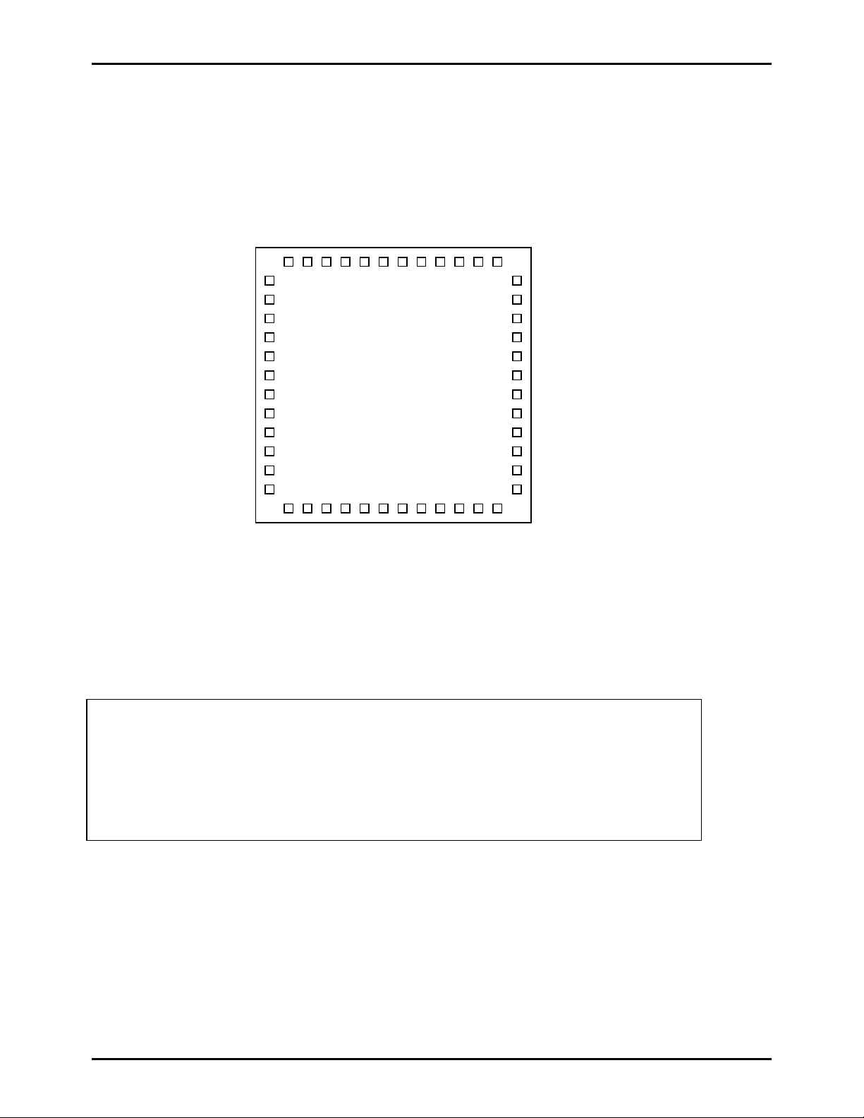
K
Pad assignment
Chip thickness : 480µm
Chip size (X × Y) : 2. 54mm × 2.27mm
Pad size : 120µm × 120µm
Pad pitch : 140µm minimum
SEG1
SEG2
SEG3
SEG4
SEG5
SEG6
SEG7
SEG8
SEG9
SEG10
SEG11
SEG12
Note:
When a Lithium battery has been selected as the power supply, please note the following points.
There are two modes of use for the lithium battery: Backup mode and Normal mode (backup flag off). In backup
mode, the battery potential is applied directly to the oscillation circuit, whereas in Normal mode only half the
battery potential is applied.
Because of the different voltage applied to the oscillation circuit in each mode, there may be a difference in the
generate d o scil lat io n fre quen cy. W hen en ter ing b ac kup mod e a c or re spo ndin g er ro r will a ris e. I f timing acc ura cy
is required (for clocks, etc), please bear in mind the above in the program design.
COM2
TEST
OSCOUT
OSCIN
RES
S1
S2
32Hz
T3
36 35 34 33 32 31 30 29 28 27 26 25
37
38
39
40
41
42
43
44
45
46
47
48
1 2 3 4 5 6 7 8 9 10 11 12
S4
S3
M1
COM3
VSS
OUT
BA
VDD2
VDD1
CUP2
M2
CUP1
COM4
COM1
SEG25
24
SEG24
23
SEG23
22
SEG22
21
SEG21
20
SEG20
19
SEG19
18
SEG18
17
SEG17
16
SEG16
15
SEG15
14
SEG14
13
SEG13
No.6726-3/18
Page 4
LC573202A
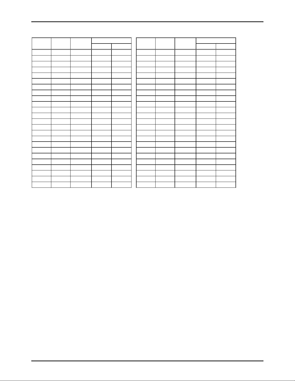
Pad name and coordinates
Pad
PIN No.
1 1 COM3 -700 -1030 25 25 COM1 840 1030
2 2 OUT -560 -1030 26 26 CUP1 700 1030
3 3 VDD2 -420 -1030 27 27 CUP2 560 1030
4 4 VDD1 -275 -1030 28 28 T3 420 1030
5 5 BAK -135 -1030 29 29 32HZ 280 1030
6 6 VSS 5 -1030 30 30 S2 140 1030
7 7 S4 145 -1030 31 31 S1 0 1030
8 8 S3 285 -1030 32 32 RES -140 1030
9 9 M1 425 -1030 33 33 OSCIN -280 1030
10 10 M2 565 -1030 34 34 OSCOUT -420 1030
11 11 COM4 705 -1030 35 35 TEST -560 1030
12 12 SEG13 845 -1030 36 36 COM2 -700 1030
13 13 SEG14 895 -775 37 37 SEG1 -895 765
14 14 SEG15 895 -635 38 38 SEG2 -895 625
15 15 SEG16 895 -495 39 39 SEG3 -895 485
16 16 SEG17 895 -355 40 40 SEG4 -895 345
17 17 SEG18 895 -215 41 41 SEG5 -895 205
18 18 SEG19 895 -75 42 42 SEG6 -895 65
19 19 SEG20 895 65 43 43 SEG7 -895 -75
20 20 SEG21 895 205 44 44 SEG8 -895 -215
21 21 SEG22 895 345 45 45 SEG9 -895 -355
22 22 SEG23 895 485 46 46 SEG10 -895 -495
23 23 SEG24 895 625 47 47 SEG11 -895 -635
24 24 SEG25 895 765 48 48 SEG12 -895 -775
No.
Pad
Name
Coordinates Coordinates QFP64
Xµm Yµm
QFP64
PIN No.
Pad
No.
Pad
Name
Xµm Yµm
• The pad coordinates are such that the chip center is taken as the origin and the va lues for (X, Y) represent the coordinates of
the center point of each pad.
• Substrate must be connected to VSS or left open.
No.6726-4/18
Page 5
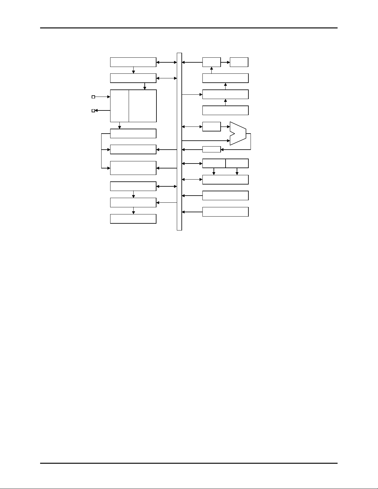
System Bl ock Diagram
HALT mode control
Stand-by control
X’tal
or
RC
Chronograph counter
Melody/buzzer
SEGMENT PLA
Clock
generator
Base timer
circuit
Strove pointer
LCD driver
LC573202A
IR PLA
ROM
PC
Stack
AC
ALU
TMP
DPL DPH
RAM
S port
M port
No.6726-5/18
Page 6
Pin Assignment
T
K
SEG1
SEG2
SEG3
SEG4
SEG5
SEG6
SEG7
SEG8
SEG9
SEG10
SEG11
SEG12
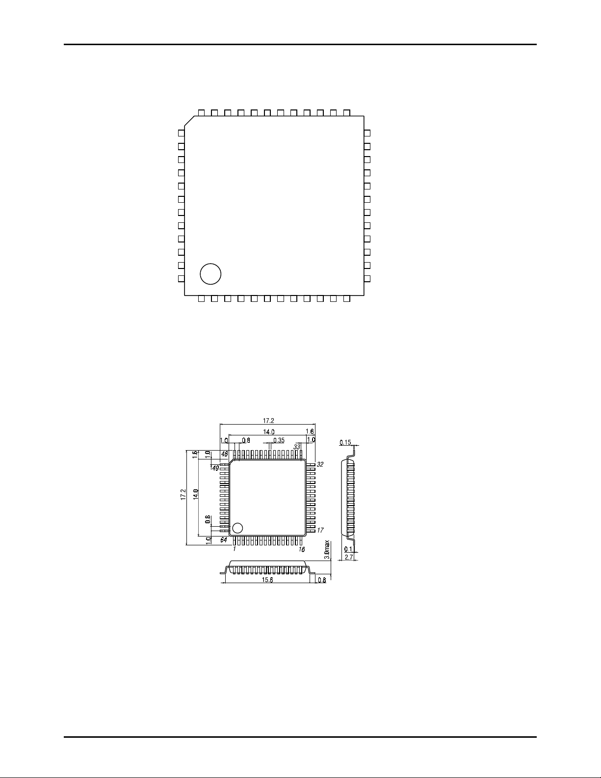
Package Dimension
(unit : mm)
3159
LC573202A
COM2
TEST
OSCOUT
OSCIN
RES
S1
S2
32Hz
T3
CUP2
36 35 34 33 32 31 30 29 28 27 26 25
37
38
39
40
41
42
43
44
45
46
47
48
1 2 3 4 5 6 7 8 9 10 11 12
S4
S3
M1
M2
COM3
OU
VSS
BA
VDD2
VDD1
CUP1
COM4
COM1
SEG25
24
SEG24
23
SEG23
22
SEG22
21
SEG21
20
SEG20
19
SEG19
18
SEG18
17
SEG17
16
SEG16
15
SEG15
14
SEG14
13
SEG13
SANYO : QIP-64E
No.6726-6/18
Page 7

LC573202A
LC573202A Terminal Description
Pin Name
VSS 6 - Power terminal(-) VDD1 4 - •Power terminal(+) (Ag battery version)
VDD2 3 - •Power terminal(+) (Li battery & EXTV version)
BAK 5 - •Power terminal(+)
CUP1, 2 26, 27 - Capacitor connecting terminals for step-up/step-down. S PORT
S1 to S4
M-PORT
M1, M2
OUT 2 O •Output terminal
SEG1 to
SEG25
COM1 to
COM4
Pad No.
Pin No.
31
30
8
7
9
10
37 to 48
12 to 24
25, 36
1, 11
I/O Function description Option
Battery version
•Voltage supply to LCD driver (Li battery & EXTV ver.)
(C is connected between VDD1 and VSS.)
•Voltage supply to logic unit (Ag battery version,
Back u p flag OFF at Li battery version.)
•Voltage supply to LCD driver (Ag battery version)
(C is connected between VDD2 an d VSS.)
•Voltage supply to logic unit (EXTV version,
Back u p flag ON at Li battery version.)
•For Li battery version, a capacitor must be connected
across BAK and VSS to prevent logic unit from
malfunctioning.
I •4-bit input port
•Input for HALT relea s e
•LSI system is reset by applying VDD* to S1 to S4
s imu ltaneously. (Mask opti on)
*Ag version : VDD1
Li/EXTV version :
VDD2
•Programmable pull-down resistor
•”L”-level hold Tr. (Mask option)
I •2-bit input port
•Input for HALT relea s e
•Programmable pull-down resistor
•”L”-level hold Tr.
•Selectable general output or buzzer output by mask
option
(1) As using general output port
•The output level is controlled by executing the SLGT
and RLGT instructions.
(2) As using buzzer output
•Melody signal or 9 kinds of modulated signal is
co ntrolled by executing the SAS or TMEL instructions.*
(Possible to output non-modulated signal)
•Possible to output 3 octave melody signal.
O •LCD output terminals for segment
•Possible to use output port for SEG13 to SEG25
(Pad No.12 to 24) by mask option.
•SEG13 can be used as COM4 output by mask option.
O •LCD output terminals fo r common
•COM4 can be used as normal output terminal by mask
option.
Ag/Li/EXTV
Battery version
Ag/Li/EXTV
-
•”L”-level hold Tr.
Provided/Not provided
•Reset by setting S1-S4
Enable/disable
•”L”-level hold Tr.
Provided/Not provided
•Output data
Melody(Buzzer)
/General output
•Output form
segment/CMOS
(SEG13-SEG25)
•Output data
SP=0-FH,
DBUS=a/b/c/d/e/f/g/h
•SEG13/COM4
•LCD duty
1/1,1/2,1/3,1/4
•COM4/LIGHT
Continue.
No.6726-7/18
Page 8

LC573202A
Pin Name
OSCIN 33 I •Input for 32.768kHz crystal oscillation
OSCOUT 34 O •Output for 32.768kHz crystal oscillation
RES 32 I Reset
TEST 35 - •Test terminal
T3 28 - •Test terminal
32Hz 29 - •Test terminal
Pad No.
Pin No.
I/O Function description Option
•Oscillation circuit
•Input for RC oscillation
•R is connected between OSCIN and OSCOUT and C is
connected between OSCIN and VSS.
•Output for RC oscillation
•R is connected between OSCIN and OSCOUT.
•This terminal should be left unconnected.
•This terminal should be left unconnected.
•This terminal should be left unconnected.
X’tal oscillation
/external RC oscillation
•Oscillation circuit
X’tal oscillation
/external RC oscillation
* 9 kinds of modulated output : For 32.768kHz crystal oscillation, proportional to oscillation frequency.
Please refer to User’s manual for mo re detail.
(Note) There are two operation modes, back-up mode (back up flag on) and normal mode (back up flag off), in Li battery
specification. In normal operation mode, the internal circuit of CPU is operated on 1/2 of Li battery voltage (it can
be monitored as external capacitor voltage of voltage step down circuit).
The power consumption can be saved in normal mode operation. However, the large current flown into/from the
buzzer output or output port will generate a voltage drop-down and it might be a cause of abnormal CPU operation.
If the microcontroller has to drive a large current, switch the CPU into the back up mode before driving the current.
CPU consumes the relatively large current in back up mode. When the Li battery voltage has recovered, you should
change the CPU into the normal m ode.
CPU is in the back up mode at reset.
No.6726-8/18
Page 9

LC573202A
p
p
p
Sample Application Circuit
(1) Ag battery used application (2) Li battery used application
(1/2 bias 1/4 duty) (1/2 bias 1/3 duty)
KEY MATRIX
32.768kHz
0.1µF
Select 4 segment
outputs as CMOS
uts
out
S1
S2
S3
S4
M1
M2
OSCIN
OSCOUT
RES
COM1
COM2
COM3
COM4
SEGOUT
VDD1
VSS
VDD2
CUP1
CUP2
OUT
0.1µF
0.1µF
1.5V(Ag)
LCD GLASS
1/2 BIAS
1/4 DUTY
KEY MATRIX
32.768kHz
0.1µF
0.1µF
Select 4 segment
outputs as CMOS
uts
out
S1
S2
S3
S4
M1
M2
OSCIN
OSCOUT
RES
BAK
COM1
COM2
COM3
SEGOUT
VDD2
VDD1
VSS
CUP1
CUP2
OUT
LCD GLASS
0.1µF
3.0V
1/2 BIAS
1/3 DUTY
GENERAL OUTPUT COM4
0.1µF
Crystal Oscillation Crystal Oscillation
(Power supply : Ag battery version) (Power supply : Li battery version)
note) COM4 is used as normal output by mask option.
(3) EXT-V used application
(1/2 bias 1/4 duty)
KEY MATRIX
Select 4 segment
outputs as CMOS
uts
out
S1
S2
S3
S4
M1
M2
32.768kHz
0.1µF
OSCIN
OSCOUT
RES
COM1
COM2
COM3
COM4
SEGOUT
VDD2
VDD1
VSS
CUP1
CUP2
OUT
0.1µF
0.1µF
3.0V
LCD GLASS
1/2 BIAS
1/4 DUTY
Crystal Oscillation
(Power supply : EXT-V version)
(Note) If LCD driver terminals (SEG13 - 25) are used for key scan output port, diodes or resistors must be added to prohibit
signal short between output ports when two or more keys are pushed simultaneously.
No.6726-9/18
Page 10

LC573202A
Ag battery version
1. Absolute Maximu m Ratings at Ta=25±2°C, VSS=0V
Parameter Symbol Pin & Conditions Ratings Unit
VDD1 -0.3 to +4.0 Supply voltage
VDD2 -0.3 to +4.0
Input voltage VIN S1-S4, M1, M2, TEST, OSCIN, RES -0.3 to VDD1+0.3
VOUT1 CUP2, OSCOUT, OUT -0.3 to VDD1+0.3 Output voltage
VOUT2 SEG1-SEG25, COM1-COM4, CUP1 -0.3 to VDD2+0.3
Peak output current
(at each pins)
Total output curre nt IALL Total outp ut pins . 10 mA
Maximum power
dissipation
Operating temperature
range
Storage temperature
range
2. Recommended Operating Range at Ta=-30°C to + 70°C, VSS=0V
Parameter Symbol Conditions
voltage
Input high voltage VIH S1-S4, RES, M1, M2 VDD1-0.2 VDD1
Input low voltage VIL S1-S4, RES, M1, M2 0 0.2
Oscillation frequency
range
[Note]
These specified value herein are based on the QIP48E packaged parts. The specification for the die is
basically the same as the one for package part. However, it will be affected by the many factors such as the
mounting board, bonding pressure, cover up epox etc.
Therefore the value specified here are only applied in Ta=25°C±2°C operating temperature range.
IOUT1 OUT 4
IOUT2 COM4 (As using LIGHT) 1
IOUT3 Output except OUT and COM4 500
Pdmax QFP48 430 mW
Topr -30 to +70
Tstg -40 to +125
Ratings
min. typ. max.
VDD1 1.30 1.65 Operating supply
VDD2 2.4 3.3
fOPG1 •32.768kHz (crystal oscillation)
•VDD1=1.30 - 1.65V
•Refer to figure 1
fOPG2 •RC oscillation
•VDD1=1.30 - 1.65V
•Refer to figure 2
32 32.768 33
30 40
Unit
kHz
V
mA
A
µ
°C
V
No.6726-10/18
Page 11

LC573202A
3. Electrical Characteristics at Ta=-30°C to + 70°C, VSS=0V
Parameter Symbol Conditions
Pull-down transistor
RIN1A VDD1=1.55V, VIL=0.2V,
Low level hold Tr. Fig.3 *1
RIN1B VDD1=1.55V,
Low level pull in Tr. Fig.3 *1
RIN2 VDD1=1.55V, TEST, RES 10 300
Output high voltage VOH1 VDD1=1.55V, IOH=-0. 4µA *2
VDD2-0.2
Output low voltage VOL1 VDD1=1.55V, IOL=0.4µA *2 0.2
Output high voltage VOH2 VDD1=1.55V, IOH=-4µA, COM1-4
Output middle voltage VOM VDD1=1.55V, IOH=-4µA, IOL=4µA,
VDD2-0.2
VDD1-0.2
COM1-4
Output low voltage VOL2 VDD1=1.55V, IOL=4µA, COM1-4
Output high voltage VOH3 VDD1=1.35V, IOH=-250µA, OUT,
VDD1-0.65
COM4 (As using LIGHT)
Output low voltage VOL3 VDD1=1.35V, IOL=150µA, OUT,
COM4 (As using LIGHT)
Output high voltage VOH4 VDD1=1.55V, IOH=-20µA *3
VDD1-0.2
Output low voltage VOL4 VDD1=1.55V, IOL=20µA *3 0.2
Step-up voltage VDD2 VDD1=1.35V, C1=C2=0.1µF,
fopg=32.768kHz, Fig.4
Current dissipation
(In Halt mode)
IDD1 VDD1=1.55V, C1=C2=0.1µF, Fig.4,
Cg=16pF, Crystal osc (CI≤25kΩ),
Back-up flag OFF, Ta≤50°C
IDD2 VDD1=1.55V, C1=C2=0.1µF, Fig.5,
RC osc (Rext=470kΩ, Cext=30pF),
Ta≤50°C
Current dissipation
(In Operating mode)
IDD3 VDD1=1.55V, C1=C2=0.1µF, Fig.4,
Cg=16pF, Crystal osc (CI≤25kΩ),
Back-up flag OFF, Ta≤50°C
IDD4 VDD1=1.55V, C1=C2=0.1µF, Fig.5,
RC osc (Rext=470kΩ, Cext=30pF),
Ta≤50°C
Oscillator start-up
voltage
Oscillator sustaining
voltage
Oscillator start-up
time
Vstt Cg=16pF, Crystal osc (CI≤25kΩ),
Back-up flag ON, Ta=25°C, Fig.6
VHOLD Cg=16pF, Crystal osc (CI≤25kΩ),
Back-up flag OFF, Ta=25°C, Fig.6
tstt VDD1=1.35V
Cg=16pF, Crystal osc(CI≤25kΩ),
Back-up flag ON, Ta=25°C, Fig.6
Ratings
min. typ. max.
150 300 1000
Unit
kΩ
100 300 1000
V
VDD1+0.2
0.2
0.65
2.5 2.7 V
1.0 4.0
A
µ
5.0 15.0
3.0 12.0
7.0 20.0
1.30
V
1.30
10 s
No.6726-11/18
Page 12

LC573202A
Li battery version
1. Absolute Maximu m Ratings at Ta=25±2°C, VSS=0V
Parameter Symbol Pin & Conditions Ratings Unit
VDD1 -0.3 to +4.0 Supply voltage
VDD2 -0.3 to +4.0
VIN1 OSCIN (Back-up flag OFF) -0.3 to VDD1+0.3 Input voltage
Peak output current
(at each pins)
Total output current IALL The total all pins. 10 mA
Maximum power
dissipation
Operating temperature
range
Storage temperature
range
2. Recommended Operating Range at Ta=-30°C to + 70°C, VSS=0V
Parameter Symbol Conditions
voltage
Input high voltage VIH S1-S4, RES, M1, M2 VDD2-0.4 VDD2
Input low voltage VIL S1-S4, RES, M1, M2 0 0.4
Oscillation frequency
range
VIN2 S1-S4, M1, M2, TEST, RES
OSCIN (Back-up flag ON)
VOUT1 CUP2, OSCOUT (Back-up flag OFF) -0.3 to VDD1+0.3 Output voltage
VOUT2 SEG1-SEG25, COM1-COM4, CUP1,
OUT, OSCOUT (Back-up flag ON)
IOUT1 OUT 4
IOUT2 COM4 (As using LIGHT) 1
IOUT3 Output except OUT and COM4 500
Pdmax QFP48 430 mW
Topr -30 to +70
Tstg -40 to +125
min. typ. max.
VDD1 1.30 3.6 Operating supply
VDD2 2.6 3.6
fOPG1 •32.768kHz (crystal oscillation)
•VDD2=2.6 - 3.6V
•Refer to figure 1
-0.3 to VDD2+0.3
-0.3 to VDD2+0.3
Ratings
32 32.768 33 kHz
V
mA
A
µ
°C
Unit
V
No.6726-12/18
Page 13

LC573202A
3. Electrical Characteristics at Ta=-30°C to + 70°C, VSS=0V
Parameter Symbol Conditions
Pull-down transistor
RIN1A VDD2=2.9V, VIL=0.4V,
Low level hold Tr. Fig.3 *1
RIN1B VDD2=2.9V,
Low level pull in Tr. Fig.3 *1
RIN2 VDD2=2.9V, TEST, RES 10 300
Output high voltage VOH1 VDD2=2.9V, IOH=-0.4µA *2
VDD2-0.2
Output low voltage VOL1 VDD2=2.9V, IOL=0.4µA *2 0.2
Output high voltage VOH2 VDD2=2.9V, IOH=-4µA, COM1-4
Output middle voltage VOM VDD2=2.9V, IOH=-4µA, IOL=4µA,
VDD2-0.2
VDD2/2
COM1-4
Output low voltage VOL2 VDD2=2.9V, IOL=4µA, COM1-4
Output high voltage VOH3 VDD2=2.4V, IOH=-250µA, OUT
VDD2-0.65
Output low voltage VOL3 VDD2=2.4V, IOL=250µA, OUT
Output high voltage VOH4 VDD2=2.4V, IOH=-150µA,
VDD2-1.5
COM4 (As using LIGHT)
Output low voltage VOL4 VDD2=2.4V, IOL=150µA,
COM4 (As using LIGHT)
Output high voltage VOH5 VDD2=2.9V, IOH=-40µA *3
VDD2-0.4
Output low voltage VOL5 VDD2=2.9V, IOL=40µA *3 0.4
Step-down voltage VDD1 VDD2=2.8V, C1=C2=0.1µF,
fopg=32.768kHz, Fig.7
Current dissipation
(In Halt mode)
Current dissipation
(In Operating mode)
Oscillator start- up
voltage
Oscillator sustaining
voltage
Oscillator start-up
time
IDD1
IDD2
Vstt Cg=16pF, Crystal osc (CI≤25kΩ),
VHOLD Cg=16pF, Crystal osc (CI≤25kΩ),
tstt VDD2=2.60V
VDD2=2.9V, C1=C2=0.1µF, Fig.7,
Cg=16pF, Crystal osc (CI≤25kΩ),
Back-up flag OFF, Ta≤50°C
VDD2=2.9V, C1=C2=0.1µF, Fig.7,
Cg=16pF, Crystal osc (CI≤25kΩ),
Back-up flag OFF, Ta≤50°C
Back-up flag ON, Ta=25°C, Fig.9
Back-up flag OFF, Ta=25°C, Fig.9
Cg=16pF, Crystal osc (CI≤25kΩ),
Back-up flag ON, Ta=25°C, Fig.9
Ratings
min. typ. max.
150 300 1000
100 300 1000
VDD2/2
-0.2
+0.2
0.2
0.65
1.5
1.35 V
0.8 2.0
1.5 5.0
2.60
2.60
10 s
Unit
kΩ
V
A
µ
V
No.6726-13/18
Page 14

LC573202A
EXT-V version
1. Absolute Maximu m Ratings at Ta=25±2°C, VSS=0V
Parameter Symbol Pin & Conditions Ratings Unit
VDD1 -0.3 to +7.0 Supply voltage
Input voltage VIN S1-S4, M1, M2, TEST, OSCIN, RES -0.3 to VDD2+0.3
Output voltage VOUT SEG1-SEG25, COM1-COM4, CUP1,
Peak output current
(at each pins)
Total output current IALL The total all pins. 10 mA
Maximum power
dissipation
Operating temperature
range
Storage temperature
range
2. Recommended Operating Range at Ta=-30°C to + 70°C, VSS=0V
Parameter Symbol Conditions
voltage
Input high voltage VIH S1-S4, RES, M1, M2 VDD2-0.4 VDD2
Input low voltage VIL S1-S4, RES, M1, M2 0 0.4
Oscillation frequency
range
VDD2 -0.3 to +7.0
-0.3 to VDD2+0.3
CUP2, OSCOUT, OUT
IOUT1 OUT 4
IOUT2 COM4 (As using LIGHT) 1
IOUT3 Output except OUT and COM4 500
Pdmax QFP48 430 mW
Topr -30 to +70
Tstg -40 to +125
Ratings
min. typ. max.
VDD1 1.3 3.0 Operating supply
VDD2 2.0 6.0
fOPG1 •32.768kHz (crystal oscillation)
•VDD2=2.0 - 6.0V
•Refer to figure 1
fOPG2 •RC oscillation
•VDD2=2.0 - 6.0V
•Refer to figure 2
32 32.768 33
30 40
V
mA
A
µ
°C
Unit
V
kHz
No.6726-14/18
Page 15

LC573202A
3. Electrical Characteristics at Ta=-30°C to + 70°C, VSS=0V
Parameter Symbol Conditions
Pull-down transistor
RIN1A VDD2=2.9V, VIL=0.4V,
Low level hold Tr. Fig.3 *1
RIN1B VDD2=2.9V,
Low level pull in Tr. Fig.3 *1
RIN2 VDD2=2.9V, TEST, RES 10 300
Output high voltage VOH1 VDD2=2.9V, IOH=-0.4µA *2
VDD2-0.2
Output low voltage VOL1 VDD2=2.9V, IOL=0.4µA *2 0.2
Output high voltage VOH2 VDD2=2.9V, IOH=-4µA, COM1-4
Output middle voltage VOM VDD2=2.9V, IOH=-4µA, IOL=4µA,
VDD2-0.2
VDD2/2
COM1-4
Output low voltage VOL2 VDD2=2.9V, IOL=4µA, COM1-4
Output high voltage VOH3 VDD2=2.4V, IOH=-250µA, OUT
VDD2-0.65
Output low voltage VOL3 VDD2=2.4V, IOL=250µA, OUT
Output high voltage VOH4 VDD2=2.4V, IOH=-150µA,
VDD2-1.5
COM4 (As using LIGHT)
Output low voltage VOL4 VDD2=2.4V, IOL=150µA,
COM4 (As using LIGHT)
Output high voltage VOH5 VDD2=2.9V, IOH=-40µA *3
VDD2-0.4
Output low voltage VOL5 VDD2=2.9V, IOL=40µA *3 0.4
Step-down voltage VDD1 VDD2=2.8V, C1=C2=0.1µF,
fopg=32.768kHz, Fig.7
Current dissipation
(In Halt mode)
IDD1
VDD2=2.9V, C1=C2=0.1µF, Fig.7,
Cg=15pF, Crystal osc (CI≤25kΩ),
Ta≤50°C
IDD2 VDD2=2.9V, C1=C2=0.1µF, Fig.8,
RC osc (Rext=470kΩ, Cext=30pF),
Ta≤50°C
Current dissipation
IDD3
VDD2=2.9V, C1=C2=0.1µF, Fig.7,
Cg=15pF, Crystal osc (CI≤25kΩ),
Ta≤50°C
IDD4 VDD2=2.9V, C1=C2=0.1µF, Fig.8,
RC osc (Rext=470kΩ, Cext=30pF),
Ta≤50°C
Oscillator start-up
voltage
Oscillator sustaining
voltage
Oscillator start-up
time
Vstt Cg=15pF, Crystal osc (CI≤25kΩ),
Ta=25°C, Fig.9
VHOLD Cg=15pF, Crystal osc (CI≤25kΩ),
Ta=25°C, Fig.9
tstt VDD2=2.0V
Cg=15pF, Crystal osc (CI≤25kΩ),
Ta=25°C, Fig.9
Ratings
min. typ. max.
150 300 1000
Unit
kΩ
100 300 1000
V
VDD2/2
-0.2
+0.2
0.2
0.65
1.5
1.35 V
3.0 15.0
A
µ
40 150
7.0 30.0
50 180
2.0
V
2.0
10 s
No.6726-15/18
Page 16

LC573202A
Electrical Characteristics at Ta=-30°C to + 70°C, VSS=0V
Parameter Symbol Conditions
Pull-down transistor
Output high voltage VOH1 VDD2=5.0V, IOH=-0.4µA *2
Output low voltage VOL1 VDD2=5.0V, IOL=0.4µA *2 0.2
Output high voltage VOH2 VDD2=5.0V, IOH=-4µA, COM1-4
Output middle voltage VOM VDD2=5.0V, IOH=-4µA, IOL=4µA,
Output low voltage VOL2 VDD2=5.0V, IOL=4µA, COM1-4
Output high voltage VOH3 VDD2=5.0V, IOH=-2.0mA, OUT
Output low voltage VOL3 VDD2=5.0V, IOL=2.0mA, OUT
Output high voltage VOH4 VDD2=5.0V, IOH=-250µA,
Output low voltage VOL4 VDD2=5.0V, IOL=250µA,
Output high voltage VOH5 VDD2=5.0V, IOH=-80µA *3
Output low voltage VOL5 VDD2=5.0V, IOL=80µA *3 0.8
Step-down voltage VDD1 VDD2=5.0V, C1=C2=0.1µF,
Current dissipation
(In Halt mode)
Current dissipation
(In Operating mode)
Oscillator start-up
voltage
Oscillator sustaining
voltage
Oscillator start-up time tstt VDD2=2.0V, Cg=15pF,
RIN1A VDD2=5.0V, VIL=0.4V,
Low level hold Tr. Fig.3 *1
RIN1B VDD2=5.0V,
Low level pull in Tr. Fig.3 *1
RIN2 VDD2=5.0V, TEST, RES 10 300
VDD2-0.2
VDD2-0.2
VDD2/2
COM1-4
VDD2-1.0
VDD2-1.5
COM4 (As using LIGHT)
COM4 (As using LIGHT)
VDD2-0.8
fopg=32.768kHz, Fig.7
IDD1
IDD2 VDD2=5.0V, C1=C2=0.1µF, Fig.8,
IDD3
IDD4 VDD2=5.0V, C1=C2=0.1µF, Fig.8,
Vstt Cg=15pF, Crystal osc (CI≤25kΩ),
VHOLD Cg=15pF, Crystal osc (CI≤25kΩ),
VDD2=5.0V, C1=C2=0.1µF, Fig.7,
Cg=15pF, Crystal osc (CI≤25kΩ,
Ta≤50°C
RC osc (Rext=470kΩ, Cext=30pF),
Ta≤50°C
VDD2=5.0V, C1=C2=0.1µF, Fig.7,
Cg=15pF, Crystal osc (CI≤25kΩ),
Ta≤50°C
RC osc (Rext=470kΩ, Cext=30pF),
Ta≤50°C
Ta=25°C, Fig.9
Ta=25°C, Fig.9
Crystal osc (CI≤25kΩ), Ta=25°C, Fig.9
Ratings
min. typ. max.
70 200 600
50 150 500
VDD2/2
-0.2
2.4 V
8.0 20.0
230 500
30 50
250 500
2.0
2.0
10 s
+0.2
0.2
1.0
1.5
*1 : S1, S2, S3, S4, M1, M2
*2 : SEG1 to SEG12 and LCD output pins out of SEG13 to SEG25.
*3 : OUTPUT PORT pins out of SEG13 to SEG2 5.
Crystal oscillation guarante ed constant
* Both Cg and Cd must be a J rank (±5%) and CH characteristics.
Oscillation type Maker Oscillator Cg
CITIZEN CFS-308 32.768kHz Crystal oscillation
SII DT-VT-200
Unit
kΩ
V
A
µ
V
No.6726-16/18
Page 17

LC573202A
(Notes) •Since the circuit pattern affects the oscillation frequency, place the oscillation-related parts as close
to the oscillation pins as possible with the shortest possible pattern length.
•If you use other oscillators herein, we provide no guarantee for the characteristics.
OSCIN OSCOUT
Cg
VSS
OSCIN OSCOUT
Rext
Cext
VSS
Figure1 Crystal oscillation circuit Figure 2 RC oscillation circuit
Program-applied
VSS
0.1µF
CUP1
CUP2
VSS
DUT
OSCIN
OSCOUT
VDD1
VDD2
Cg
0.1µF
Figure3 Input configuration of Figure 4 Current dissipation, step-up voltage
S1-4, M1, M2 measurement
0.1µF
CUP1
CUP2
VSS
DUT
OSCIN
OSCOUT
VDD1
VDD2
Rext
Cext
0.1µF
CUP2
VSS
DUT
OSCIN
OSCOUT
VDD1
VDD2
Cg
Figure5 Current dissipation, step-up Figure 6 Oscillator start-up voltage, oscillator
voltage measurement start-up time, oscillator sustaining
voltage measurement
No.6726-17/18
Page 18

LC573202A
0.1µF
0.1µF
BAK
CUP1
CUP2
VSS
DUT
OSCIN
OSCOUT
VDD1
VDD2
0.1µF
Cg
0.1µF
CUP1
CUP2
VSS
DUT
OSCIN
OSCOUT
VDD2
VDD1
Rext
Figure7 Current dissipation, step-down Figure 8 Current dissipation, step-down
voltage measurement voltage measurement
CUP2
VSS
DUT
OSCIN
OSCOUT
BAK
VDD1
VDD2
Cg
Figure9 Oscillator start-up voltage, oscillator
start-up time, oscillato r susta ini ng
voltage measurement
Cext
0.1µF
No.6726-18/18
PS
 Loading...