

Page 1

Any and all SANYO products described or contained herein do not have specifications that can handle
applications that require extremely high levels of reliability, such as life-support systems, aircraft’s
control systems, or other applications whose failure can be reasonably expected to result in serious
physical and/or material damage. Consult with your SANYO representative nearest you before using
any SANYO products described or contained herein in such applications.
SANYO assumes no responsibility for equipment failures that result from using products at values that
exceed, even momentarily, rated values (such as maximum ratings, operating condition ranges,or other
parameters) listed in products specifications of any and all SANYO products described or contained
herein.
CMOS IC
4-bit Single Chip Microcontroller
Ordering number:ENN*4144
LC573104A, 573102A
SANYO Electric Co.,Ltd. Semiconductor Company
TOKYO OFFICE Tokyo Bldg., 1-10, 1 Chome, Ueno, Taito-ku, TOKYO, 110-8534 JAPAN
Preliminary
Overview
LC573104A and LC573102A are CMOS 4-bit
microcontrollers featuring low-voltage operation and low
power dissipation.
Both LC573104A and LC573102A incorporate a 4-bit parallel processing ALU, 4K bytes/2K bytes ROM, a 64×4-bit
RAM, a 16-bit timer, and an infrared remote control transmission carrier output circuit.
Applications
• Remote controller.
• Control of small measuring instruments.
Features
• ROM :4096×8 bits (LC573104A)
• RAM : 64×4 bits
• Cycle time
elcyC
emit
sµ6.71
2048×8 bits (LC573102A)
kcolcmetsyS
rotareneg
noitallicsocimareC
tiucric
noitallicsO
ycneuqerf
zHk554V0.6ot3.2
ylppuS
egatlov
Package Dimensions
unit:mm
3112A-MFP24S
[LC573104A, 573102A]
24
112
Pin Assignment
12.5
0.35
13
5.4
0.15
1.7max
1.5
0.1
1.0
(0.75)
7.6
0.63
SANYO : MFP24S
• Current Drain
a. At normal operation
tnerruC
niard
pytAµ051noitallicsoRCzHk554V0.3
pytAµ004noitallicsoRCzHk554V0.5
kcolcmetsyS
rotareneg
noitallicsO
ycneuqerf
ylppuS
egatlov
b. HALT mode
tnerruC
niard
pytAµ08noitallicsoRCzHk554V0.3
pytAµ003noitallicsoRCzHk554V0.5
kcolcmetsyS
rotareneg
noitallicsO
ycneuqerf
ylppuS
egatlov
c. HOLD mode
egakaeL
tnerruc
pytAµ1.0
noitidnoC
noitallicsoRCnehW
edomPOTStasi
noitallicsO
ycneuqerf
zHk554V0.5
ylppuS
egatlov
O1501TN (KT)/13195JN/5252JN No.4144–1/16
Page 2

LC573104A, 573102A
• Port
· Input port (S port, M port) : 2-port (8 pins) [Key scan input port]
· Input/Ouput port : 3-port (10 pins)
P0 port, P1 port 2-port (8 pins) [Key scan output port]
P2 port 1-port (2 pins) [Key scan expansion port]
[LED direct drivable port]
• Infrared remote control carrier generation circuit.
·Software-controllable remote control carrier output ON/OFF.
·Software-controllable carrier frequency and duty ratio.
<38kHz-1/3 duty, 38kHz-1/2 duty, 57kHz-1/2 duty>
(When fixed carrier signal is output, it is specified by mask option)
·1kHz to 200kHz infrared remote control transmission carrier frequency.
(When carrier output is selected by timer at mask option, and when 455kHz CR oscillator is used)
·Infrared carrier output-dedicated terminal built-in (CA terminal).
·108ms HALT-mode cancel signal output.
• Timer
·16-bit software-controllable Timer
Timer input clock : Ceramic (CR) oscillation frequency (455kHz).
·108ms HALT release request signal generation timer (Free running timer).
·Watchdog timer (changed over between USED/UNUSED by mask option)
• Sub-routine stack level
·2 levels
• Oscillation circuit
·Ceramic (CR) oscillation circuit : 455kHz (for System clock generation), Feedback resistor built-in.
• Standby function
·HALT mode
HALT mode used to reduce current drain.
HALT mode suspends program execution.
Following shows how to release the HALT mode.
(A) System reset
(B) HALT mode release request signal.
·HOLD mode
HOLD mode stops ceramic resonator (CR). The HOLD mold can be released in two ways.
(A) System reset
(B) Apply H level input to S port pin or M port pin. (However, it is necessary to set S port or M port HOLD mode
release permission flag beforehand.)
• From of shipment
·MFP-24S (1.0mm pitch) and chip.
NOTE : When dipping in solder to mount the MFP package on board, contact SANYO for instructions.
No.4144–2/16
Page 3
LC573104A, 573102A
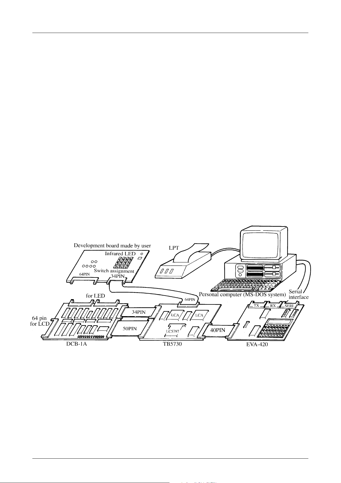
The Application Development System for the LC573100 Series.
(1) Manual
(A) Users Manual : LC573100 Series Users Manual.
(B) Development Tool Manual : LC573100 Series Development Tool Manual.
(2) Development Tools
• Tools for application development of the LC573100 Series.
(A) Personal computer (MS-DOS based).
(B) Cross assembler (LC573100.EXE).
(C) Mask option generator (SU573100.EXE).
• Tools to evaluate application development of the LC573100 Series.
(A) EVA chip (LC5797).
NOTE 1) As RAM capacity differs between EVA chip (LC5797) and the LC573100 Series, always check before pro-
gramming and debugging.
LC573100 : 64×4 bits
LC5797 : 256×4 bits
NOTE 2) Always keep the DPH value in mind when programming. Only DPH ‘0’ to ‘3’ may be used as the RAM
address.
If DPH other than ‘0’ to ‘3’ is used as RAM address when pro gramming, SANYO will not be liable for any
trouble caused.
(B) EVA chip board (TB5730).
NOTE) The application evaluation board is the evaluation board made by the user.
(C) Evaluation board [EVA420 (Monitor ROM : ER-573000)]
(D) Display and mask option data control board [DCB-1A (REV3.6)]
Development Support System Outline
Do not cross or twist these cables.
No.4144–3/16
Page 4
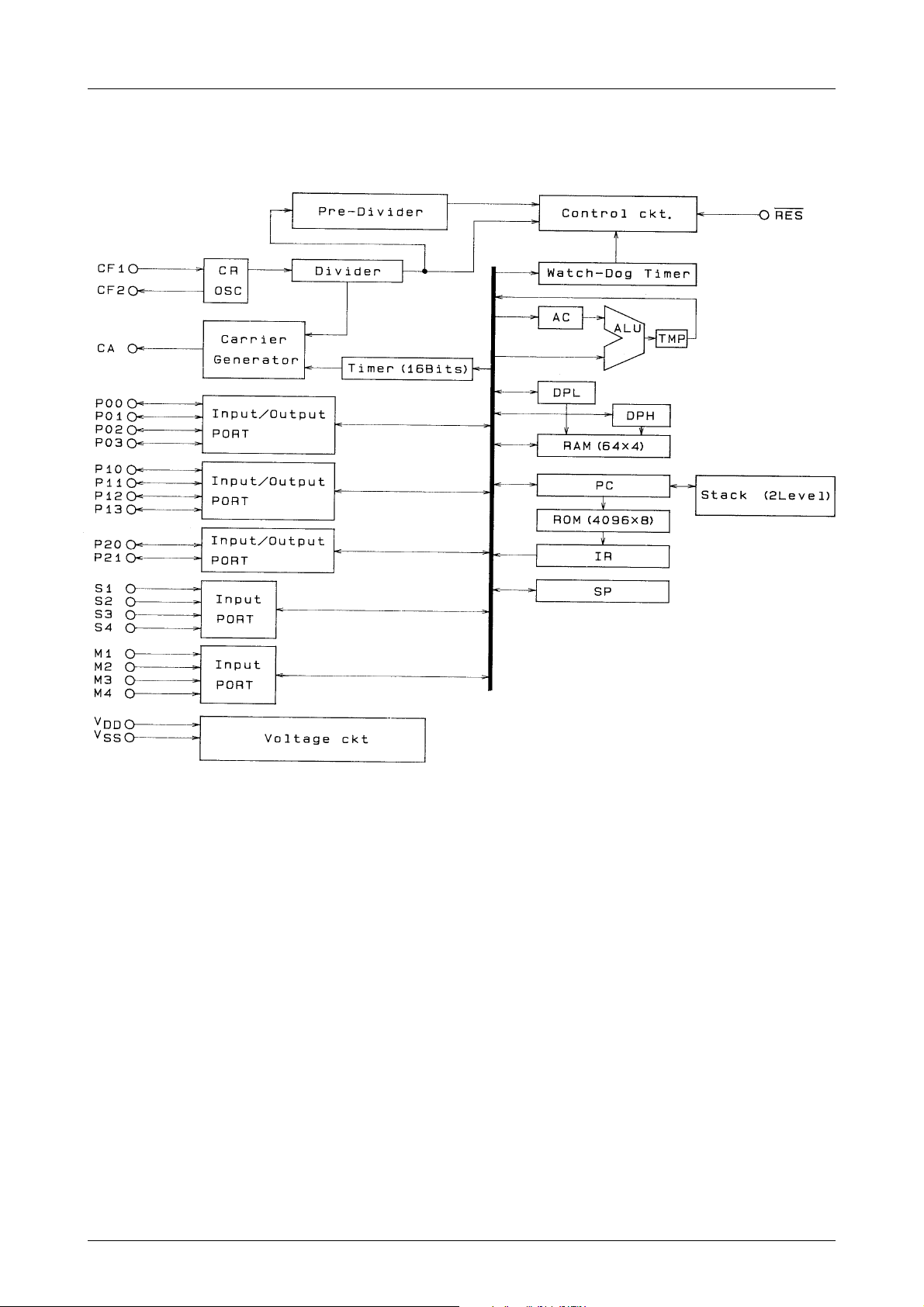
(A) Block Diagram
(LC573104A)
LC573104A, 573102A
No.4144–4/16
Page 5
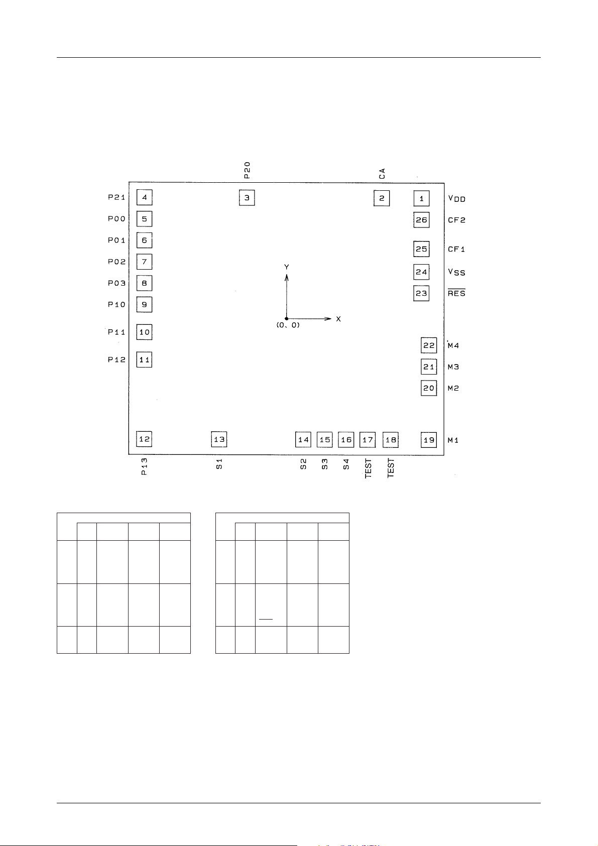
Die Specifications
Pad Layout
LC573104A, 573102A
Chip size : 3.51mm×3.19mm
Chip thickness : 480µm
Pad size : 120µm×120µm
Pad coordinates
MFP24S pin assignment
Pad
Pin
No.
Name
17
1
V
18
19
20
21
22
23
24
1
2
3
4
5
DD
2
CA
3
P20
4
P21
5
P00
6
P01
7
P02
8
P03
9
P10
10
P11
11
P12
12
P13
13
S1
X
(µm)Y(µm)
1465
1155
– 305
–1485
–1485
–1485
–1485
–1485
–1485
–1485
–1485
–1485
– 410
– 220
– 480
–1395
–1395
1365
1365
1365
1365
1110
870
565
325
20
MFP24S pin assignment
Pad
Pin
No.
Name
6
14
7
8
–
–
9
10
11
12
13
14
15
16
S2
15
S3
16
S4
17
TEST
18
TEST
19
M1
20
M2
21
M3
22
M4
23
RES
24
V
SS
25
CF1
26
CF2
X
(µm)Y(µm)
360
–1395
560
–1395
760
–1395
960
–1395
1140
–1395
1560
–1395
1560
– 905
1560
– 685
1560
– 445
1465
1465
1465
1465
330
570
755
1155
• The chip center is the origin of the above pad coordinates.
The X, Y values represent the coordinate of the pad center.
• When dipping the MFP24S package in solder to mount on boards, contact SANYO for instructions, etc.
• Chip substrate should be connected to VSS or left open.
No.4144–5/16
Page 6

Pin Function
LC573104A, 573102A
MFP24S
Pin No.
17 V
14 V
15 CF1 Input
16 CF2 Output
5
6
7
8
9
10
11
12
21
22
23
24
1
2
3
4
19
20
18 CA Output Remote control carrier output.
13 RES Input Reset input. Internal pull-up resistor.
Pin
Input/
name
Output
– Supply voltage. See Fig 1.
DD
– Ground. See Fig 1.
SS
S1
S2
S3
S4
M1
M2
M3
M4
P00
P01
P02
P03
P10
P11
P12
P13
P20
P21
User for system clock oscillation.
• 455kHz ceramic resonator is connected between CF1 and
CF2 for oscillation.
• Stops oscillation when receiving CR oscillation stop command.
Input
Input port S.
• LSI system is reset by charging VDD to S1 to S4
simultaneously (Mask option).
• Data is loaded in accumulator.
Input
Input port M.
Data loaded in accumulator.
Input/
Input/output port.
Output
• Data loaded in accumulator.
• Output pin to output data from accumulator.
(P-ch Open Drain Output)
Input/
Input/output port.
Output
• Data loaded in accumulator.
• Output pin to output data from accumulator.
(P-ch Open Drain Output)
Input/
Input/output port.
Output
• Data loaded in accumulator.
• Output pin to output data from accumulator.
(P-ch Open Drain Output)
• LED direct drivable pin.
Option Reset statusFunction description
(1) 'L' level HOLD Tr
YES/NO
(2) Reset by S1 to S4.
'L' level HOLD Tr YES/NO • Pull-down resistor ON.
Fixed carrier output/
Carrier output by timer
• Pull-down resistor ON.
• Reset signal ENABLE.
• At reset 'L' level.
• At fixed carrier output
38kHz-1/3 duty.
No.4144–6/16
Page 7

Supply connections
LC573104A, 573102A
Fig. 1 Supply connections
No.4144–7/16
Page 8

LC573104A, 573102A
Mask Option
(1) Input port option
Option Remarks
'L' level Hold
Tr selection
(2) Reset signal option by S port
Option Remarks
Resetting IC by
S port
Circuit
Next port switches over in
sequence.
• S1 to S4, M1 to M4
Input signal level
Hold Tr selection
• 'L' level Hold Tr used.
• 'L' level Hold Tr not used.
Circuit
Selects signal for resetting IC
system by simultaneously charging
'H' level to S1 to S4.
• Allow
• Prohibit
(3) Carrier standard clock generation circuit option for remote control
Option Remarks
38/57kHz Software-controllable carrier
Timer 8 bit
overflow
Circuit
frequency and duty.
• Following carrier frequency and
duty may be selected by setting
control register 4.
(1) 38kHz-1/3 Duty
(2) 38kHz-1/2 Duty
(3) 57kHz-1/2 Duty
Timer 8-bit overflow signal
generates carrier signal for infrared
remote control.
No.4144–8/16
Page 9

LC573104A, 573102A
(4) Watchdog timer circuit option
Option Remarks
Watchdog
timer selection
Circuit
Watchdog timer used/unused
selection
Specifications
Absolute Maximum Ratings
retemaraPlobmySsnoitidnoCsgnitaRtinU
V
egatlovylppuS
egatlovtupnIV
egatlovtuptuOV
tnerructuptuO
)nip1reP(
ACtpecxesnipllafotnerructuptuolatoTI
erutarepmetgnitarepOrpoT 07+ot03–
erutarepmetegarotSgtsT 521+ot04–
DD
V
1DD
V
2DD
NI
TUO
I
1TUO
I
2TUO
I
3TUO
I
4TUO
LLA
)edom
)edomtuptuoera12P,02P,31Pot01P,30P
)nip1rep(AC 52Am
)nip1rep(31Pot01P,30Pot00P 005Aµ
)nip1reP(12P,02P 01Am
)nip1rep(evobadetsilnahtrehtosniptuptuO 005Aµ
)nipACroftpecxe(delatotsnipllA 52Am
,02P,31Pot01P,30Pot00P,SER,4Mot1M,4Sot1S
tupniera12P,02P,31Pot01P,30Pot00P(1FC,12P
ot00P(2FC,12P,02P,31Pot01P,30Pot00P,AC
0.7+ot3.0–V
Vot3.0–
DD
Vot3.0–
DD
Vot3.0–
3.0+V
DD
Vot3.0–
3.0+V
DD
V
V
˚C
˚C
Recommended Operating Ranges at Ta =–30 to +70˚C, VSS=0V
retemaraPlobmySsnoitidnoC
egatlovylppuSV
egatlovlevel-hgihtupnIV
egatlovlevel-woltupnIV
egatlovlevel-hgihtupnIV
egatlovlevel-woltupnIV
ycneuqerfnoitarepOf
DD
1HI
1LI
2HI
2LI
GPO
SER
2.giF,noitallicsoRCtA083554005zHk
Fig. 2 CR Oscillation Circuit
sgnitaR
nimpytxam
3.20.6V
V7.0
)edomtupnierastrop2P,1P,0P(12P
,02P,31Pot01P,30Pot00P,4Mot1M,4Sot1S
DD
0
V57.0
DD
0
V
V3.0
V
V52.0
tinU
V
DD
V
DD
V
DD
V
DD
No.4144–9/16
Page 10

LC573104A, 573102A
Electrical Characteristics at Ta =–30 to +70˚C, VSS=0V
retemaraPlobmySsnoitidnoC
RNIA1
ecnadepmitupnI
egatlovlevel-hgihtuptuOV
tnerruckael-ffotuptuO
egatlovlevel-hgihtuptuOV
tnerruckael-ffotuptuO
)H(tnerructuptuOI
)L(tnerructuptuOI
tnerrucylppusedom-TLAHI
tnerrucgnitarepOI
1tnerruckaelylppuSI
2tnerruckaelylppuSI
egatlovpu-tratsrotallicsOV
egatlovgniniatsusrotallicsOV
emitpu-tratsrotallicsOt
RNIB1
RNI2V
I
I
I
I
V
V
1VDDI,V9.2=
HO
FFO
V
FFO
2VDDI,V9.2=
HO
FFO
V
FFO
1VDDV,V0.3=
HO
1VDDV,V0.3=
LO
V
1
DD
aT ≤ 05° 5.giF,C
V
2
DD
aT ≤ 05° 5.giF,C
1
KAEL
V
205=aT°C 1 5Aµ
KAEL
TS
SUS
V
TS
V,V9.2=
DD
DD
DD
DD
DD
DD
DD
DD
DD
4.giF
LI
3.giF,rTdloH
V,V9.2=
LI
SER,V9.2=01003kΩ
HO
HO
HOV=DD
HO
V0.3=
nimpytxam
level'L',4Mot1M,4Sot1S,V4.0=
3.giF,rTnwod-llup
31Pot01P,30Pot00P,V9.2=
12P,02P,Am01–=V
12P,02P,V9.2=
AC,V5.1–621Am
AC,V9.0=25Am
level'L',4Mot1M,4Sot1S,V4.0=
31Pot01P,30Pot00P,Aµ054–=
VNIV=
SS
VNIV=
DD
VNIV=
SS
VNIV=
DD
,Fp051=gcC=dcC,noitallicsoRCzHk554,V0.3=
,Fp051=gcC=dcC,noitallicsoRCzHk=554,V0.3=
52=aT°C 2.01Aµ
4.giF,noitallicsoRCzHk554,Fp051=gcC=dcC
,noitallicsoRCzHk554,Fp051=gcC=dcC,V3.2=
0510030001kΩ
0305001kΩ
V
54.0–
DD
0.1–Aµ
5.0–V
DD
0.1–Aµ
0.2V
sgnitaR
0.1Aµ
0.1Aµ
08003Aµ
051005Aµ
3.2V
03sm
tinU
V
Electrical Characteristics at Ta =–30 to +70˚C, VSS=0V
retemaraPlobmySsnoitidnoC
RNIA1
ecnadepmitupnI
egatlovlevel-hgihtuptuOV
tnerruckael-ffotuptuO
egatlovlevel-hgihtuptuOV
tnerruckael-ffotuptuO
)H(tnerructuptuOI
)L(tnerructuptuOI
tnerrucylppusedom-TLAHI
tnerrucgnitarepOI
1tnerruckaelylppuSI
2tnerruckaelylppuSI
egatlovpu-tratsrotallicsOV
egatlovgniniatsusrotallicsOV
emitpu-tratsrotallicsOt
RNIB1
RNI2V
I
I
I
I
V
V
1VDDI,V0.5=
HO
FFO
V
FFO
2VDDI,V0.5=
HO
FFO
V
FFO
1VDDV,V0.5=
HO
1VDDV,V0.5=
LO
V
1
DD
aT ≤ 05° 5.giF,C
V
2
DD
aT ≤ 05° 5.giF,C
1
KAEL
V
205=aT°C 1 5Aµ
KAEL
TS
SUS
V
TS
V,V0.5=
DD
DD
3.giF
DD
DD
DD
DD
DD
DD
DD
4.giF
LI
3.giF,rTdloH
SER,V0.5=01003kΩ
HO
HO
HOV=DD
LO
V0.5=
Recommended Oscillators.
rotallicsOrerutcafunaMrebmuntraPgcCdcC
cimareczHk554
rotallicso
31Pot01P,30Pot00P,V0.5=
12P,02P,Am01–=V
12P,02P,V0.5=
AC,V5.2–0102Am
AC,V9.0=25Am
arecoyKY/KB554-RBKFp051Fp051
ataruME554BSCFp051Fp051
scimareCijuF554-EOPFp051Fp051
sgnitaR
nimpytxam
level'L',4Mot1M,4Sot1S,V4.0=
,rTnwod-lluplevel'L',4Mot1M,4Sot1S,V0.5=
31Pot01P,30Pot00P,Aµ057–=
VNIV=
SS
VNIV=
DD
VNIV=
SS
VNIV=
DD
,Fp051=gcC=dcC,noitallicsoRCzHk554,V0.5=
,Fp051=gcC=dcC,noitallicsoRCzHk554,V0.5=
52=aT°C 2.01Aµ
4.giF,noitallicsoRCzHk554,Fp051=gcC=dcC
,noitallicsoRCzHk554,Fp051=gcC=dcC,V3.2=
07002006kΩ
0305001kΩ
V
57.0–
DD
0.1–Aµ
5.0–V
DD
0.1–Aµ
003004Aµ
004005Aµ
0.2V
tinU
V
0.1Aµ
0.1Aµ
3.2V
03sm
No.4144–10/16
Page 11

Fig. 3 : S1 to S4, M1 to M4 input structure
Fig. 5 : Supply current measuring circuit
LC573100 Series Instruction Set
LC573104A, 573102A
Fig. 4 : Oscillator start-up voltage, Oscillator sustaining
voltage, and Oscillator start-up time measuring
circuit.
Note : CR is 455kHz, S-PORT : M-PORT : Input lead Tr is ON.
RES terminal has resistor built-in and is OPEN.
I/O-PORT is set at Output Mode and data is ‘H’.
The instruction set uses the following abbreviations and symbols.
AC : Accumulator M : Memory
ACn : Accumulator bit n M (DP) : Memory addressed by DP
CF : Carry flag [M (DP)] : Contents of memory addressed by DP
DP : Data pointer PC : Program counter
DPL : Data pointer low nibble PCn : Program counter bit n
DPH : Data pointer high nibble PAGE : Page latch
EDP : Data pointer save register STSn : Status register n
EDPL : Data pointer save register low nibble (STSm) : Status register n content
EDPH : Data pointer save register high nibble [P ( )] : Contents of port ( )
SP : Strobe pointer X : Immediate data
TREG : Temporary register Xn : Immediate data bit n
SCFn : Start conditioning flag n PDF : Input port pull-down flag
CTLn : Control register n SFR : Special function register
HEFn : Hold enable flag n (SFR) : Contents of special function register
ROM : ROM data CSTF : Chrono start flag
CFCF : Ceramic resonator oscillator control flag SPC : Strobe pointer control bit
( ) : Contents CCF : Carrier output control flag
[ ] : Contents ( ) : Complement of contents
∨ : Logical OR [ ] : Complement of contents
∨ : Logical exclusive-OR φ n : Output from stage n of 15-stage divider
<
: Logical AND WDT : Watchdog timer
← : Transfer direction, result
• The special function registers are abbreviated as follows.
TCON : Timer control register
TLOW : Timer/counter reg ister low byte
THIGH : Timer/counter register high byte
CTL4 : Control register 4
P0 : Port P0
P1 : Port P1
P2 : Port P2
No.4144–11/16
Page 12

LC573104A, 573102A
LC573100 Series Instructions
Mnemonic Instruction code Function
Instruction
TAAT 0 0 0 0 0 0 0 1 AC, TRGE ← ROM 1 2 Contents of ROM on current page, addressed by PC whose low-orderd 8 bits
MTR 0 0 0 1 0 0 1 0 M (DP) ← TREG 1 1 Stores the conternts of TREG memory location pointed to by DP.
Bytes
Cycles
are replaced with contents of AC and M (DP), are loaded to AC and TREG
Function description
Status
flag
affected
ASR0 0 0 0 1 1 0 0 0 ACn ← AC
ASR1 0 0 0 1 1 0 0 1 ACn ← AC
ASL0 0 0 0 1 1 0 1 0 ACn ← AC
AccumulatorLogical Arithmetic
ASL1 0 0 0 1 1 0 1 1 ACn ← AC
INC 1 0 0 1 1 0 0 0 AC, M (DP) ← M (DP)+1 1 1 Memory M (DP) contents incremented +1, and loaded to AC and M (DP).
DEC 1 0 0 1 1 0 0 1 AC, M (DP) ← M (DP)–1 1 1 Memory M (DP) contents decremented –1, and loaded to AC and M (DP).
ADC 1 0 0 0 0 0 0 0 AC ← (AC)+[M (DP)]+CF 1 1 AC, memory M (DP) and CF contents are binary-added and the result loaded
ADC* 1 0 0 0 1 0 0 0 AC, M (DP) ← (AC)+[M (DP)]+CF 1 1 AC, memory M (DP) and CF contents are binary-added and the result loaded
ADCI X 1 0 0 1 0 0 0 0
– – – – X3X2X1X
SBC 1 0 0 0 0 0 0 1 AC ← (AC)+[M (DP)]+CF 1 1 AC, memory M (DP) and CF contents are binary-subtracted, and the result
SBC* 1 0 0 0 1 0 0 1 AC, M (DP) ← (AC)+[M (DP)]+CF 1 1 AC, memory M (DP) and CF contents are binary-subtracted, and the result
SBCI X 1 0 0 1 0 0 0 1
– – – – X3X2X1X
ADD 1 0 0 0 0 0 1 0 AC ← (AC)+[M (DP)] 1 1 AC and memory M (DP) contents are binary-added and the result loaded to
ADD* 1 0 0 0 1 0 1 0 AC, M (DP) ← (AC)+[M (DP)] 1 1 AC and memory M (DP) contents are binary-added and the result loaded to
ADDI X 1 0 0 1 0 0 1 0
– – – – X3X2X1X
SUB 1 0 0 0 0 0 1 1 AC ← (AC)+[M (DP)]+1 1 1 AC and memory M (DP) contents are binary-subtracted and the result loaded
SUB* 1 0 0 0 1 0 1 1 AC, M (DP) ← (AC)+[M (DP)]+1 1 1 AC and memory M (DP) contents are binary-subtracted and the result loaded
SUBI X 1 0 0 1 0 0 1 1
– – – – X3X2X1X
ADN 1 0 0 0 0 1 0 0 AC ← (AC)+[M (DP)] 1 1 AC and memory M (DP) contents are binary-added and the result loaded to
ADN* 1 0 0 0 1 1 0 0 AC, M (DP) ← (AC)+[M (DP)] 1 1 AC and memory M (DP) contents are binary-added and the result loaded to
ADNI X 1 0 0 1 0 1 0 0
– – – – X3X2X1X
AND 1 0 0 0 0 1 0 1 AC ← (AC) [M (DP)] 1 1 AC and memory M (DP) contents are ANDed and the result loaded to AC.
AC ← (AC)+X+CF 2 2 AC, immediate data and CF contents are binary-added, and the result loaded
0
AC ← (AC)+X+CF 2 2 AC, immediate data and CF contents are binary-subtracted and the result
0
AC ← (AC)+X 2 2 AC and immediate data contents are binary-added and the result loaded to
0
AC ← (AC)+X+1 2 2 AC and immediate data contents are binary-subtracted and the result loaded in
0
AC ← (AC)+X 2 2 AC and immediate data contents are binary-added and the result loaded in AC.
0
, AC3 ← 0 1 1 Shifts the contents of the AC right and enter 0 into the MSB.
n+1
, AC3 ← 1 1 1 Shifts the contents of the AC right and enter 1 into the MSB.
n+1
, AC0 ← 0 1 1 Shifts the contents of the AC left and enter 0 into the LSB.
n–1
, AC0 ← 1 1 1 Shifts the contents of the AC left and enter 1 into the LSB.
n–1
to AC.
to AC, M (DP).
to AC.
loaded to AC.
loaded to AC and M (DP).
loaded to AC.
AC.
AC and M (DP).
AC.
to AC.
to AC and M (DP).
AC.
AC.
AC and M (DP).
CF
CF
CF
CF
CF
CF
CF
CF
CF
CF
CF
CF
AND* 1 0 0 0 1 1 0 1 AC, M (DP) ← (AC) [M (DP)] 1 1 AC and memory M (DP) contents are ANDed and the result loaded to AC and
ANDI X 1 0 0 1 0 1 0 1
– – – – X3X2X1X
EOR 1 0 0 0 0 1 1 0 AC ← (AC) ∨ [M (DP)] 1 1 AC and memory M (DP) are exclusive ORed and the result loaded to AC.
EOR* 1 0 0 0 1 1 1 0 AC, M (DP) ← (AC) ∨ [M (DP)] 1 1 AC and memory M (DP) are exclusive ORed, and the result loaded to AC and
EORI X 1 0 0 1 0 1 1 0
– – – – X3X2X1X
OR 1 0 0 0 0 1 1 1 AC ← (AC) ∨ [M (DP)] 1 1 AC and memory M (DP) are ORed and the result loaded to AC.
OR* 1 0 0 0 1 1 1 1 AC, M (DP) ← (AC) ∨ [M (DP)] 1 1 AC and memory M (DP) are ORed and the result loaded to AC and M (DP).
ORI X 1 0 0 1 0 1 1 1
– – – – X3X2X1X
AC ← (AC) X 2 2 AC and immediate data contents are ANDed and the result loaded to AC.
0
AC ← (AC) ∨ X 2 2 AC and immediate data are exclusive ORed and the result loaded to AC.
0
AC ← (AC) ∨ X 2 2 AC and immediate data are ORed and the result loaded to AC.
0
M (DP).
M (DP).
Continued on next page.
No.4144–12/16
Page 13

LC573104A, 573102A
Continued from preceding page.
Mnemonic Instruction code Function
Instruction
SDPL 0 0 0 1 1 1 0 0 DPL ← (AC) 1 1 AC contents loaded to DPL.
SDPH 0 0 0 1 1 1 0 1 DPH ← (AC) 1 1 AC contents loaded to DPH.
LDPL 1 1 1 1 1 1 0 1 AC ← (DPL) 1 1 DPL contents loaded to AC.
LDPH 1 1 1 1 1 1 1 0 AC ← (DPH) 1 1 DPH contents loaded to AC.
MDPL X 1 0 1 1 X3X2X1X0DPL ← X 1 1 Immediate data X loaded to DPL.
MDPH X 1 1 0 0 X3X2X1X0DPH ← X 1 1 Immediate data X loaded to DPH.
EDPL 0 0 0 1 1 1 1 0 (DPL) ↔ (EDPL) 1 1 DPL and EDPL contents exchanged.
Data PointerFlagData transfer SP
EDPH 0 0 0 1 1 1 1 1 (DPH) ↔ (EDPH) 1 1 DPH and EDPH contents exchanged.
IDPL 1 0 0 1 1 0 1 0 DPL ← (DPL)+1 1 1 DPL contents incremented +1.
IDPH 1 0 0 1 1 1 0 0 DPH ← (DPH)+1 1 1 DPH contents incremented +1.
DDPL 1 0 0 1 1 0 1 1 DPL ← (DPL)–1 1 1 DPL contents decremented –1.
DDPH 1 0 0 1 1 1 0 1 DPH ← (DPH)–1 1 1 DPH contents decremented –1.
Bytes
Cycles
Function description
Status
flag
affected
SSP 1 0 1 0 1 1 1 0 SP ← (AC) 1 1 AC contents loaded to SP.
LSP 1 0 1 0 1 0 1 0 AC ← (SP) 1 1 SP contents loaded to AC.
MSP X 1 1 1 0 X3X2X1X0SP ← X 1 1 Immediate data X loaded to SP.
ISP 1 0 0 1 1 1 1 0 SP ← (SP)+1 1 1 SP contents incremented +1.
DSP 1 0 0 1 1 1 1 1 SP ← (SP)–1 1 1 SP contents decremented –1.
LHLT 1 0 1 0 1 0 1 1 AC ← (STS2), STS2 ← 0 1 1 STS2 contents loaded to AC and STS2 is reset.
L500 1 0 1 0 1 1 0 0 AC ← (STS1), SCF0 ← 0 1 1 STS1 contents loaded to AC and SCF0 is reset.
CSP 0 0 0 0 0 1 0 0 CSTF ← 0 1 1 CSTF reset.
CST 0 0 0 0 0 1 0 1 CSTF ← 1 1 1 CSTF set.
RC5 0 0 0 0 0 1 1 0 HEF0 ← 0 1 1 HEF0 reset to inhibit Halt mode release by overflow from the divider circuit.
SC5 0 0 0 0 0 1 1 1 HEF0 ← 1 1 1 HEF0 set enabling overflow from the divider circuit to release the Halt mode.
RCF 1 1 1 1 0 0 0 0 CF ← 0 1 1 CF reset.
SCF 1 1 1 1 0 0 0 1 CF ← 1 1 1 CF set.
LDA 1 0 1 0 1 0 0 1 AC ← [M (DP)] 1 1 Memory M (DP) contents transferred to AC.
STA 1 0 1 0 1 1 0 1 M (DP) ← (AC) 1 1 AC contents stored in memory M (DP).
SCF1 to
SCF4
SCF0
CSTF
CSTF
HEF0
HEF0
CF
CF
LDI X 0 0 1 1 X3X2X1X0AC ← X 1 1 Immediate data X loaded to AC.
MVI X 0 0 1 0 X3X2X1X0M (DP) ← X 1 1 Immediate data X loaded to memory M (DP).
Continued on next page.
No.4144–13/16
Page 14

LC573104A, 573102A
Continued from preceding page.
Mnemonic Instruction code Function
Instruction
HALT 0 0 0 0 0 0 0 0 CPU operation halts 1 1 • Halts CPU operation. HALT mode is released under the following conditions.
SCI X 1 1 0 1 X3X2X1X0CTL2 ← X11X
CPU controlInput/Output
NOP 1 1 1 1 1 1 1 1 No operation 1 1 No operation.
IPS 1 0 1 0 1 1 1 1 AC ← [P (S)] 1 1 Input data at input port S loaded to AC.
IPM 1 0 1 0 1 0 0 0 AC ← [P (M)] 1 1 Input data at input port M loaded to AC.
Bytes
Cycles
• HALT mode is cancelled by the interaction of SIC X and SC5 commands.
to X3Operation.
0
X0HFE1 is set to enable release of HALT mode by overflow signal
from divider circuit following CF oscillation circuit.
X1HFE2 is set enabling signal rise at input port S to release HALT
mode.
X2HFE3 is set enabling signal rise at input port M to release HALT
mode.
X3HFE4 is set enabling 1/10 second pulse to release HALT.
Function description
Status
flag
affected
HEF1 to
HEF4
SPDR X 1 1 1 1 0 1 X1X0PDF ← X 1 1 Pull-down resister MOS-Tr at corresponding input port turned ON/OFF.
Bit content Operation
X0=0 S-Terminal Pull down Tr OFF.
X0=1 S-Terminal Pull down Tr ON.
X1=0 M-Terminal Pull down Tr OFF.
X1=1 M-Terminal Pull down Tr ON.
OUT 1 1 1 1 1 1 0 0 (1) Cannot be used when SPC
=0&SP=0H to CH, EH, FH.
(2) When SP=0&SP=D
CTL3 ← (AC)
(3) When SPC=1 SFR ← (AC) AC contents transferred to special function register SFR.
TWRT 0 0 0 0 0 0 1 0 (1) Cannot be used when SPC
=0&SP=0H to CH, EH, FH.
(2) When SPC=0&SP=D
CTL3 ← ROM
(3) When SPC=1 SFR ← ROM High-order 4 bits or 8 bits data of ROM, on the current page, addressed by PC
IN 0 0 0 1 0 1 1 1 (1) Cannot be used at SPC
=0&SP=0H to CH, EH, FH.
(2) When SPC=0&SP=D
AC ← (STS3)
(3) When SPC=1 AC ← (SFR) Special function register SFR contents transferred to AC.
1 1 Cannnot be used. (Causes error when OUT is executed at SPC=0&SP=0H to
CH, EH, FH.)
AC contents transferred to CTL3.
1 1 Cannnot be used. (Causes error when TWRT is executed at SPC=0&SP=0H to
CH, EH, FH.)
High-order 4 bits data of ROM, on current page, addressed by PC whose low-
order 8 bits are replaced by AC and M (DP) contents, is transferred to CTL3.
whose low-order 8 bits are replaced by AC and M (DP) contents is transferred
to special function register SFR
1 1 Cannnot be used. (Causes error when IN is executed at SPC=0&SP=0H to
CH, EH, FH.)
STS3 contents transferred to AC.
PDF
CFCF
CCF
CFCF
CCF
Continued on next page.
No.4144–14/16
Page 15

LC573104A, 573102A
Continued from preceding page.
Mnemonic Instruction code Function
Instruction
JMP X
BAB0 X
BAB1 X
BAB2 X
BAB3 X
BAZ X
BANZ X
BCNH X
BCH X
Branching/subroutineMiscellaneous
PAGE 0 0 0 1 0 0 0 1 PAGE ← [M (DP)] 1 1 Memory M (DP) contents loaded to PAGE latch.
0 0 0 0 1 X10X9X
X7X6X5X4X3X2X1X
0 1 0 0 1 X10X9X
X7X6X5X4X3X2X1X
0 1 0 1 1 X10X9X
X7X6X5X4X3X2X1X
0 1 1 0 1 X10X9X
X7X6X5X4X3X2X1X
0 1 1 1 1 X10X9X
X7X6X5X4X3X2X1X
0 1 0 0 0 X10X9X
X7X6X5X4X3X2X1X
0 1 0 1 0 X10X9X
X7X6X5X4X3X2X1X
0 1 1 0 0 X10X9X
X7X6X5X4X3X2X1X
0 1 1 1 0 X10X9X
X7X6X5X4X3X2X1X
(PC10 to PC0) ← X10 to X
8
0
If AC0=1 then
8
(PC10 to PC0) ← X10 to X
0
If AC1=1 then
8
(PC10 to PC0) ← X10 to X
0
If AC2=1 then
8
(PC10 to PC0) ← X10 to X
0
If AC3=1 then
8
(PC10 to PC0) ← X10 to X
0
If AC=0 then
8
(PC10 to PC0) ← X10 to X
0
If AC≠0 then
8
(PC10 to PC0) ← X10 to X
0
If CF≠1 then
8
(PC10 to PC0) ← X10 to X
0
If CF=1 then
8
(PC10 to PC0) ← X10 to X
0
0
0
0
0
0
0
0
0
0
Bytes
Cycles
2 2 Loads data specified by X10 to X0 to PC and jumps unconditionally.
2 2 When AC bit 0 is '1', data specified by X10 to X0 is loaded to PC and jumps.
At '0', PC is incremented +2.
2 2 When AC bit 1 is '1', data specified by X10 to X0 is loaded to PC and jumps.
At '0', PC is incremented +2.
2 2 When AC bit 2 is '1', data specified by X10 to X0 is loaded to PC and jumps.
At '0', PC is incremented +2.
2 2 When AC bit 3 is '1', data specified by X10 to X0 is loaded to PC and jumps.
At '0', PC is incremented +2.
2 2 When AC is '0', data specified by X10 to X0 is loaded to PC and jumps.
When AC is not '0', PC is incremented +2.
2 2 When AC is not '0', data specified by X10 to X0 is loaded to PC and jumps.
When AC is '0', PC is incremented +2.
2 2 When CF is '0', data specified by X10 to X0 is loaded to PC and jumps.
When CF is '1', PC is incremented +2.
2 2 When CF is '1', data specified by X10 to X0 is loaded to PC and jumps.
When CF is '0', PC is incremented +2.
Function description
Status
flag
affected
JMP* 0 0 0 1 0 0 0 0 PC10 to PC08 ← (PAGE)
ROM0 1 1 0 0 1 0 0 0
ROM1 1 1 0 0 1 0 0 0
JSR X
RST 0 0 0 1 0 0 1 1 PC ← (STACK) 1 1 Returns PC contents saved in STACK to PC and returns from sub-routine.
SPC0 1 1 0 0 1 0 0 1
SPC1 1 1 0 0 1 0 0 1
CSEC 1 1 1 1 1 0 1 1 φ11 to φ15 ← 0 1 1 Resets high-order 4 bits of divider circuit.
RWDT 1 1 1 1 1 0 0 1 (WDT) ← 0 1 1 Resets Watchdog Timer counter.
0 0 1 0 0 0 0 0
0 0 1 0 0 0 0 1
1 0 1 0 0 X10X9X
X7X6X5X4X3X2X1X
0 0 1 0 0 0 0 0
0 0 1 0 0 0 0 1
PC07 to PC04 ← (AC)
PC03 to PC00 ← [M (DP)]
PC11 ← 0 2 2 Select ROM bank 0.
PC11 ← 1 2 2 Select ROM bank 1.
STACK ← (PC)+2
8
(PC10 to PC0) ← X10 to X
0
SPC ← 0 2 2 Resets strobe pointer control bit (SPC) to '0'.
SPC ← 1 2 2 Sets strobe pointer control bit (SPC) to '1'.
0
1 1 Unconditionally jumps to page specified by PAGE and address whose low-
order 8 bits are specified by contents of AC and memory M (DP).
2 2 Current PC+2 contents are saved in STACK, data specified by X10 to X0 is
loaded to PC and sub-routine is called.
SPC
SPC
SCF0
SCF4
No.4144–15/16
Page 16

LC573104A, 573102A
LC573100 Series Instructions Map
rewoL
rewppU
0TLAH TAATTRWT –PSCTSC5CR5CS
1*PMJEGAPRTMSTR –––NI0RSA1RSA0LSA1LSALPDSHPDSLPDEHPDE
2 XIVM
3 XIDL
4
5
6
7
8CDACBSDDABUSNDADNAROERO*CDA*CBS*DDA*BUS*NDA*DNA*ROE*RO
9
A
B XLPDM
CXHPDM–
D XCIS
E XPSM
FFCRFCSPONPONXRDPS–TDWR–CESCTUOLPDLHPDLPON
0123456789ABCDEF
XPMJ
XZAB X0BAB
XHNCB X1BAB
XHNCB X2BAB
XHCB X3BAB
ICDA ICBS IDDA IBUS INDA IDNA IROE IROCNICEDLPDILPDDHPDIHPDDPSIPSD
XRSJMPIADLPSLTLHL005LATSPSSSPI
XMOR XCPS–
: 1 Byte-1 Cycle instruction ROMX : ROM0 instruction (C820H),
XXX
ROM1 instruction (C821H)
: 2 Byte-2 Cycle instruction SPCX : SPC0 instruction (C920H),
XXX
SPC1 instruction (C921H)
: 1 Byte-2 Cycle instruction
XXX
Specifications of any and all SANYO products described or contained herein stipulate the performance,
characteristics, and functions of the described products in the independent state, and are not guarantees
of the performance, characteristics, and functions of the described products as mounted in the customer's
products or equipment. To verify symptoms and states that cannot be evaluated in an independent device,
the customer should always evaluate and test devices mounted in the customer's products or equipment.
SANYO Electric Co., Ltd. strives to supply high-quality high-reliability products. However, any and all
semiconductor products fail with some probability. It is possible that these probabilistic failures could
give rise to accidents or events that could endanger human lives, that could give rise to smoke or fire,
or that could cause damage to other property. When designing equipment, adopt safety measures so
that these kinds of accidents or events cannot occur. Such measures include but are not limited to protective
circuits and error prevention circuits for safe design, redundant design, and structural design.
In the event that any or all SANYO products(including technical data,services) described or
contained herein are controlled under any of applicable local export control laws and regulations,
such products must not be exported without obtaining the export license from the authorities
concerned in accordance with the above law.
No part of this publication may be reproduced or transmitted in any form or by any means, electronic or
mechanical, including photocopying and recording, or any information storage or retrieval system,
or otherwise, without the prior written permission of SANYO Electric Co. , Ltd.
Any and all information described or contained herein are subject to change without notice due to
product/technology improvement, etc. When designing equipment, refer to the "Delivery Specification"
for the SANYO product that you intend to use.
Information (including circuit diagrams and circuit parameters) herein is for example only ; it is not
guaranteed for volume production. SANYO believes information herein is accurate and reliable, but
no guarantees are made or implied regarding its use or any infringements of intellectual property rights
or other rights of third parties.
This catalog provides information as of October, 2001. Specifications and information herein are subject
to change without notice.
PS No.4144–16/16
 Loading...