

Page 1

Overview
The LC4105V is a level shifter driver that converts 5-V
signals into signals with amplitudes between 10 and 18 V.
Features
• Seven inputs and eleven outputs
IN1 to IN3 produce only true outputs.
IN4 to IN7 produce both true and inverted outputs.
• Slim SSOP-30 package
Package Dimensions
unit: mm
3191-SSOP30
CMOS LSI
43098HA(OT)/13097HA(OT) No. 5641-1/6
SANYO: SSOP30
[LC4105V]
SANYO Electric Co.,Ltd. Semiconductor Bussiness Headquarters
TOKYO OFFICE Tokyo Bldg., 1-10, 1 Chome, Ueno, Taito-ku, TOKYO, 110-8534 JAPAN
Level Shifter
LC4105V
Ordering number : EN5641A
Specifications
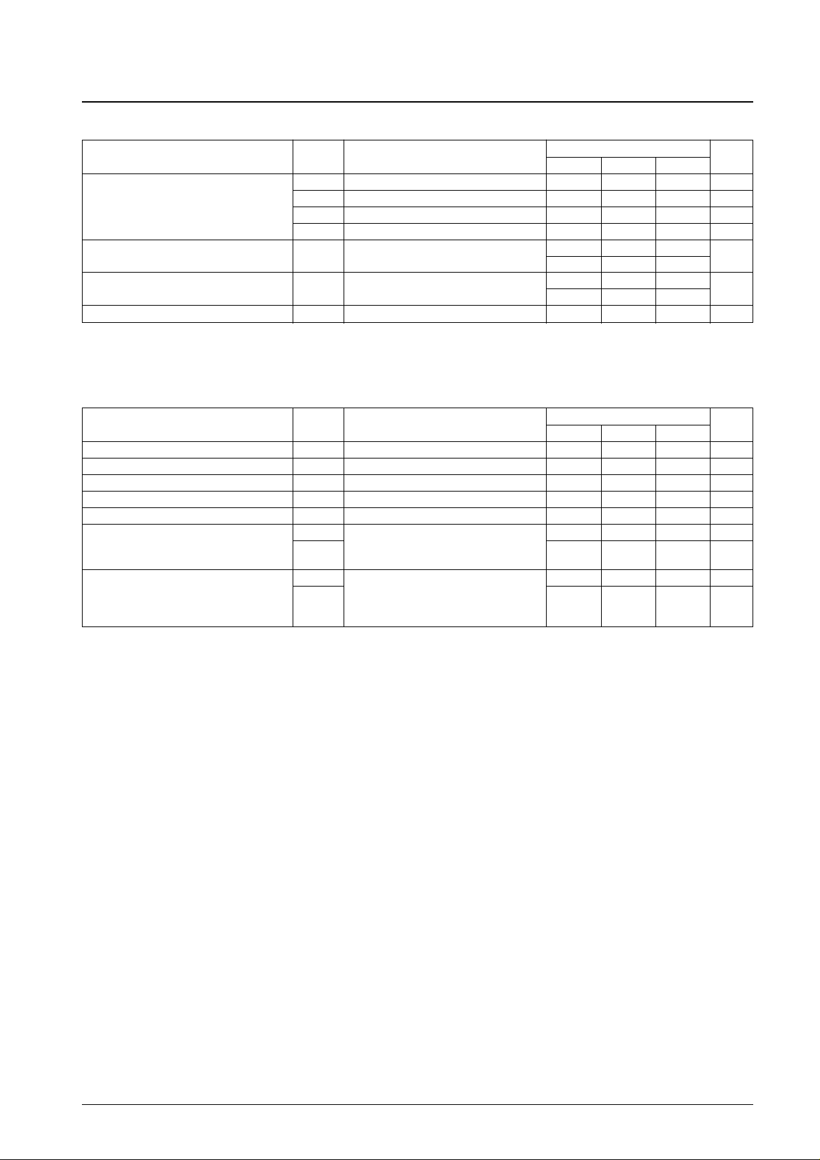
Absolute Maximum Ratings at Ta = 25°C ± 2°C, all voltages are relative to VSS, unless otherwise specified
Parameter Symbol Conditions
Ratings
Unit
min typ max
V
DD
–0.3 20 V
Power supply voltage
V
DD
1 –0.3 20 V
V
CC
–0.3 7 V
V
SS
1 –0.3 +0.3 V
Input voltage V
IN
IN1 to IN7 –0.5 VCC+0.5 V
Power dissipation Pd Ta ≤ 75°C 200 mW
Storage temperature Tstg –55 +125 °C
Page 2
No. 5641-2/6
LC4105V
Parameter Symbol Conditions
Ratings
Unit
min typ max
V
DD
* 10 18 V
Power supply voltage
V
DD
1 * V
DD
V
V
CC
* 3.0 5.5 V
V
SS
1 * V
SS
V
High-level input voltage V
IN
-H
IN1 to IN7 (VCC= 4.5 to 5.5 V) 2.4 V
CC
V
(V
CC
= 3.0 to 4.5 V)
0.7 V
CC
V
CC
Low-level input voltage VIN-L
IN1 to IN7 (VCC= 4.5 to 5.5 V) 0 0.8
V
(V
CC
= 3.0 to 4.5 V)
0 0.1 V
CC
Operating temperature Topr –10 +75 °C
Allowable Operating Ranges at voltages relative to V
SS
Note: * Applications must observe the directions in the note on page 5 at power on and at power off.
Note: * I
DD
I and IDDa are the total currents flowing into power supply pins VDDand VDD1.
Parameter Symbol Conditions
Ratings
Unit
min typ max
High-level input current I
ih
Vin = VCCIN1 to IN7 1 µA
Low-evel input current I
il
Vin = VSSIN1 to IN7 –1 µA
High-level output voltage V
oh
Io = 1 mA VDD–1 V
DD
V
Low-level output voltage V
ol
Io = –1 mA V
SS
VSS+1 V
Output on resistance Rout V
DD
= VDD1 = 10 V Io = ±1 mA 60 Ω
Current drain while idling
I
CCI
VDD= VDD1 = 18 V, VCC= 5.5 V 0.01 10 µA
I
DDI
*
IN1 to IN7 = 0 V
0.10 10 µA
. All outputs open.
I
CCa
VDD= VDD1 = 15 V, VCC= 5.5 V
16 µA
Current drain during operation
IN0 to IN6 = 0 V
I
DDa
* IN7 = 0 to 5.5 V/2 MHz 10 mA
Load 1
Electrical Characteristics
at Ta = 25°C ±2°C, VCC= 5 V, and VDD= 16 V, all voltages are relative to VSS, unless othrewise specified
Page 3

Pin Assignment Block Diagram
Pin Descriptions
No. 5641-3/6
LC4105V
Pin Name I/O Pin Number Function
OUT1 28
OUT2 27
OUT3 26
OUT4 25
OUT4* 24
OUT5 O 23 Level shifter outputs
OUT5* 22
OUT6 21
OUT6* 20
OUT7 19
OUT7* 18
IN1 5
IN2 6
IN3 7
IN4 I 8 Level shifter inputs
IN5 9
IN6 10
IN7 11
V
DD
— 1 Level shifter high-voltage power supply
V
DD
1 — 30 Buffer high-voltage power supply
V
CC
— 2 Level shifter low-voltage power supply
V
SS
1 — 15, 16 Buffer ground
V
SS
— 14 Level shifter ground
NC 3, 4, 12, 13, 17, 29 Do not connect anything to these pins.
Page 4

No. 5641-4/6
LC4105V
Switching Characteristics at Ta = 25°C ±2°C, VCC= 5 V ±10%, VDD= 10 to 18 V
Parameter Symbol Conditions
Ratings
Unit
min typ max
tpLH(1) 33 60 ns
Propagation delay
tpHL(1)
Load 1
35 60 ns
tpLH(2) tpHL(1)–10 36 tpHL(1)+20 ns
tpHL(2) tpLH(1)–20 20 tpLH(1)+10 ns
Rising time tr Load 1 24 50 ns
Falling time tf Load 1 24 50 ns
Parameter Symbol Conditions
Ratings
Unit
min typ max
tpLH(1) 100 ns
Propagation delay
tpHL(1)
Load 1
120 ns
tpLH(2) 120 ns
tpHL(2) 100 ns
Rising time tr Load 1 50 ns
Falling time tf Load 1 50 ns
at Ta = 25°C ±2°C, VCC= 3.0 to 4.5 V, VDD= 10 to 18 V
Load 1
Note: The typical values are measured for OUT1 output with VCC= 5.5 V and VDD= 15 V.
Page 5

No. 5641-5/6
LC4105V
Power Supply Circuits
Keep the impedance of the VSSand VSS1 lines as low as possible. Connect a large electrolytic capacitor across the VDD1
and VSS1 pins and close to the IC. Wherever possible, keep the grounds for the power supply circuits and the signal
circuits separate and connect the two at a single point.
Notes on Power-Supply Voltage Application
This IC has two power supply systems: VDD(VDD1) and VCC, and requires that applications observe the notes provided
here when applying or removing these voltages. In particular, if the VDD(VDD1) system power-supply voltage becomes
higher than the VCCsystem voltage while the VCCsystem voltage is not yet established (i.e. is less than VCCmin),
excessive currents may flow and the IC may be destroyed. To prevent destruction of the IC due to this phenomenon,
applications must, basically, follow the sequence described in item 1 below when turning the power supplies on or off.
1. When turning the power on, first apply the VCCvoltage (bring this voltage to a value above VCCmin), and then apply
the VDDvoltage. When turning the power off, first drop the VDDvoltage, and, after VDDis below VCCmin, then drop
the V
CC
voltage.
Power-supply voltage
Time
V
DD,VDD
1
V
CC
Page 6

PS No. 5641-6/6
LC4105V
This catalog provides information as of April, 1998. Specifications and information herein are subject to change
without notice.
■ No products described or contained herein are intended for use in surgical implants, life-support systems, aerospace
equipment, nuclear power control systems, vehicles, disaster/crime-prevention equipment and the like, the failure of
which may directly or indirectly cause injury, death or property loss.
■ Anyone purchasing any products described or contained herein for an above-mentioned use shall:
➀ Accept full responsibility and indemnify and defend SANYO ELECTRIC CO., LTD., its affiliates, subsidiaries and
distributors and all their officers and employees, jointly and severally, against any and all claims and litigation and all
damages, cost and expenses associated with such use:
➁ Not impose any responsibility for any fault or negligence which may be cited in any such claim or litigation on
SANYO ELECTRIC CO., LTD., its affiliates, subsidiaries and distributors or any of their officers and employees
jointly or severally.
■ Information (including circuit diagrams and circuit parameters) herein is for example only; it is not guaranteed for
volume production. SANYO believes information herein is accurate and reliable, but no guarantees are made or implied
regarding its use or any infringements of intellectual property rights or other rights of third parties.
However, there are many cases where it is not possible to control the power-supply voltage on/off sequence. This IC is
actually capable of supporting the on/off sequence described in item 2 below.
2. If VDD(VDD1) and VCCare turned on and off at essentially the same time, the difference between VDDand VCC(e.g.
the distance in the figure marked as ∆0.5 V) must be held to be under 0.5 V while VCCis less than or equal to 3.0 V.
Another point is that a certain amount of time is required to stabilize the VCCsystem when VCCis first applied and the
IC is easily destroyed during this period. Inversely, when the power is removed, the VCCsystem state is easily retained
and as a result the device cannot be destroyed easily. In actual use, one can consider there to be a certain amount of
margin for removing the VDD(VDD1) voltage even after VCChas already been dropped. However, this margin varies
with sample-to-sample variations in the IC itself and with the details of the application circuit, and careful analysis and
consideration of the actual usage conditions is required to assure that the IC will not be destroyed if the sequences in
items 1 or 2 are not observed.
3. Note that when power is turned off and then immediately turned back on again, many circuit designs may fail to meet
the conditions for the sequences described in items 1 and 2 above. Be sure to take this into account when designing
applications that use this IC.
Power-supply voltage
Time
V
DD,VDD
1
V
CC
 Loading...