

Page 1
Overview
The LC378100QM and LC378100QT are 1,048,576-word
× 8-bit organization (8,388,608-bit) mask programmable
read only memories. They feature a wide operating
voltage range (2.6 to 5.5 V), a 100-ns access time (tCA) at
VCC= 4.5 to 5.5 V, and a 200-ns access time at VCC= 2.6
to 3.3 V. Thus these LSIs can be used in a wide range of
systems, from 5-V systems that require high-speed access
to 3-V systems that use batteries.
Features
• 1048576 words × 8 bits organization
• Supply voltage range: 2.6 to 5.5
• Fast access time(tAA):120 ns (max.) VCC= 4.5 to 5.5 V
(tCA): 100 ns (max.) VCC= 4.5 to 5.5 V
200 ns (max.) VCC= 2.6 to 5.5 V
• Operating current 55 mA (max.)
• Standby current 30 µA (max.)
• Full static operation (internal clocked type)
• 3 state outputs
• JEDEC standard pin configuration
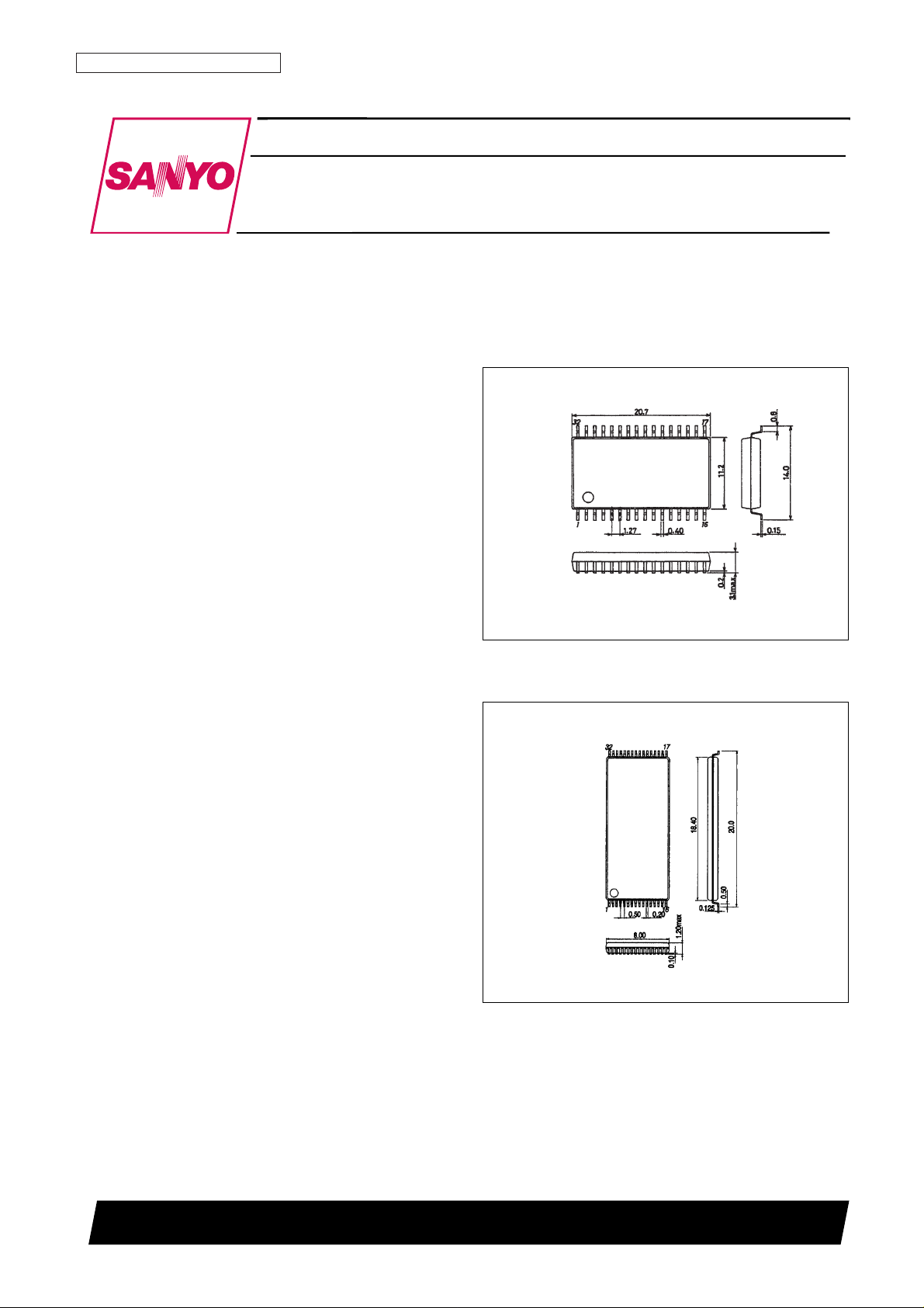
• Package type
LC378100QM: SOP32 (525 mil)
LC378100QT: TSOP32 (8 mm × 20 mm)
Package Dimensions
unit: mm
3205-SOP32
unit: mm
3224-TSOP32
CMOS IC
53098HA (OT) No. 5611-1/4
Preliminary
SANYO Electric Co.,Ltd. Semiconductor Bussiness Headquarters
TOKYO OFFICE Tokyo Bldg., 1-10, 1 Chome, Ueno, Taito-ku, TOKYO, 110-8534 JAPAN
8 MEG (1048576 words × 8 bits) Mask ROM
Internal Clocked Silicon Gate
LC378100QM, QT
Ordering number : EN*5611A
SANYO: SOP32
[LC374100QM]
SANYO: TSOP32 (type-I)
[LC374100QT]
Page 2

CE OE Output Current drain
H X High-impedance Standby mode
L H High-impedance Operating mode
L L DOUT Operating mode
No. 5611-2/4
LC378100QM, QT
Pin Assignments
Block Diagram
Truth Table
Pin Functions
A0 to A16 Address input
D0 to D7 Data output
CE Chip enable input
OE Output enable input
V
CC
Power supply
V
SS
Ground
X: H or L level should be offered.
Page 3

No. 5611-3/4
LC378100QM, QT
Parameter Symbol Conditions Ratings Unit
Supply voltage V
CC
–0.3 to +7.0 V
Supply input voltage V
IN
–0.3*2to VCC+ 0.3 V
Supply output voltage V
OUT
–0.3 to VCC+ 0.3 V
Allowable power dissipation Pd max Ta = 25°C; Reference values for the SANYO DIP package 1.0 W
Operating temperature Topr –10 to +70 °C
Storage temperature Tstg –55 to +125 °C
Specifications
Absolute Maximum Ratings *1
Note: 1. Permanent device damage may occur if Absolute Maximum Ratings are exceeded. Functional operation should be restricted to Recommended
Operating Conditions.
2. V
IN
(min) = –3.0 V (pulse width ≤ 30 ns)
Note: 1. t
OD
is measured from the earlier edge of the CE or OE’s going high impedance.
This parameter is periodically sampled and not 100% tested.
2. Guaranteed at V
CC
= 4.5 to 5.5 V
Note: * This parameter is periodically sampled and not 100% tested.
Note: * Guaranteed at Ta = 25°C
Parameter Symbol Conditions
Ratings
Unit
min typ max
Input capacitance C
IN
VIN= 0 V; Reference values for the SANYO DIP package 8 pF
Output capacitance C
OUTVOUT
= 0 V; Reference values for the SANYO DIP package 10 pF
Input/Output Capacitance* at Ta = 25°C, f = 1.0 MHz
Parameter Symbol Conditions
Ratings
Unit
min typ max
Supply voltage V
CC
2.6 5.0 5.5 V
Input high level voltage V
IH
2.2 VCC+ 0.3 V
Input low level voltage V
IL
–0.3 +0.6 V
DC Recommended Operating Ranges at Ta = –10 to +70°C, VCC= 2.6 to 5.5 V
Parameter Symbol Conditions
Ratings
Unit
min typ max
Operating supply current
I
CCA1
CE = 0.2 V, VI= VCC– 0.2 V/0.2 V 30 mA
I
CCA2
CE = VIL, IO= 0 mA, VI= VIH/VIL, f = 10 MHz 55 mA
Standby supply current
I
CCS1
CE = VCC– 0.2 V 30 (1.0) µA
I
CCS2
CE = V
IH
1.0 (300) mA(µA)
Input leakage current I
LI
VIN= 0 to V
CC
±1.0 µA
Output leakage current I
LO
CE or OE = VIH, V
OUT
= 0 to V
CC
±1.0 µA
Output high level voltage V
OHIOH
= –0.5 mA 0.8 V
CC
V
Output low level voltage V
OLIOL
= 0.5 mA 0.2 V
DC Electrical Characteristics at Ta = –10 to +70°C, VCC= 2.6 to 5.5 V
Parameter Symbol Conditions
Ratings
Unit
min typ max
Cycle time t
CYC
200 (120) ns
Address access time t
AA
200 (120) ns
CE access time t
CA
200 (100) ns
OE access time t
OA
80 (40) ns
Output hold time t
OH
20 ns
Output disable time
*1
tOD*1 100 ns
AC Characteristics at Ta = –10 to +70°C, VCC= 2.6 to 5.5 V
Page 4

PS No. 5611-4/4
LC378100QM, QT
Timing Chart
This catalog provides information as of May, 1998. Specifications and information herein are subject to change
without notice.
■ No products described or contained herein are intended for use in surgical implants, life-support systems, aerospace
equipment, nuclear power control systems, vehicles, disaster/crime-prevention equipment and the like, the failure of
which may directly or indirectly cause injury, death or property loss.
■ Anyone purchasing any products described or contained herein for an above-mentioned use shall:
➀ Accept full responsibility and indemnify and defend SANYO ELECTRIC CO., LTD., its affiliates, subsidiaries and
distributors and all their officers and employees, jointly and severally, against any and all claims and litigation and all
damages, cost and expenses associated with such use:
➁ Not impose any responsibility for any fault or negligence which may be cited in any such claim or litigation on
SANYO ELECTRIC CO., LTD., its affiliates, subsidiaries and distributors or any of their officers and employees
jointly or severally.
■ Information (including circuit diagrams and circuit parameters) herein is for example only; it is not guaranteed for
volume production. SANYO believes information herein is accurate and reliable, but no guarantees are made or implied
regarding its use or any infringements of intellectual property rights or other rights of third parties.
System Design Notes
These LSIs adopt the ATD technique, in which operation starts when a change in either the CE or address inputs is
detected. This means that the output data immediately after power is applied is invalid. When using these LSIs as
program memory for Z80 and similar microprocessors, applications must take into account the fact that valid data will
not be output after power is first applied unless the value of either the CE or at least one of the address lines is changed
after the power supply has stabilized.
Another point due to the use of the ATD technique is that these LSIs are sensitive to input noise. Do not apply voltages
outside the allowable DC input levels for extended periods and do not apply input voltages with large noise components.
AC Test Conditions
Input pulse levels 0.4 to 2.8 V
Input rise/fall time 5 ns
Input timing level 1.5 V
Output timing level 1.5 V
Output load See Figure 1
Figure 1 Output Load
 Loading...