

Page 1
Overview
The LC374500ST is a 524288-word × 8-bit (4M) mask
programmable ROM that is pin compatible with flash
memory. Since this product supports the wide operating
voltage range of 2.6 to 5.5 V and achieves access times of
100 ns (tCA) when VCCis between 4.5 and 5.5 V and 200
ns when VCCis between 2.6 and 5.5 V, it can be used both
in high-speed 5-V systems and battery-operated 3-V
systems. Since this product is pin compatible with flash
memory it can replace flash memory used during
prototyping and production.
Features
• 524288-word × 8-bit organization
• Wide supply voltage range: 2.6 to 5.5 V
• Access times (tAA): 120 ns (maximum) at VCC= 4.5 to
5.5 V
(tCA): 100 ns (maximum) at VCC= 4.5 to
5.5 V
200 ns (maximum) at VCC= 2.6 to
5.5 V
• Operating supply current: 50 mA (maximum)
• Standby mode supply current: 30 µA (maximum)
• Fully static operation (internal synchronization)
• Three-state outputs
• Pin compatible with flash memory
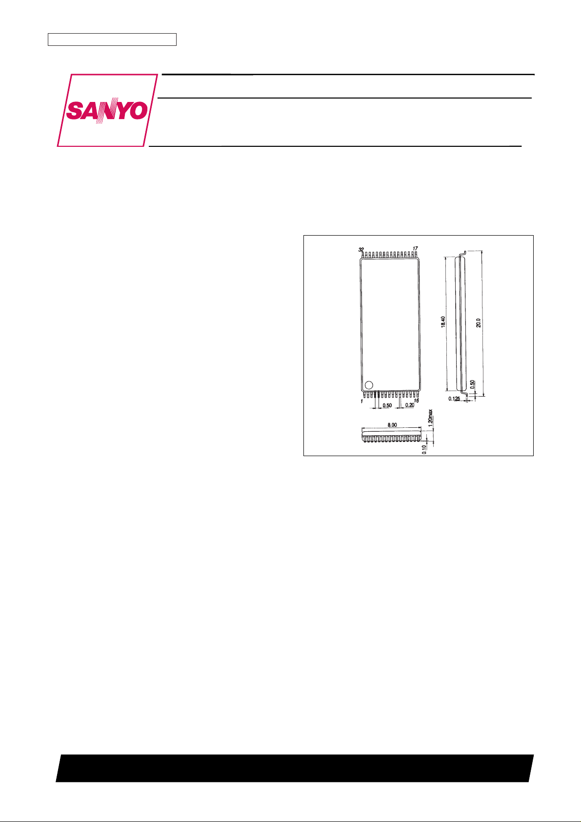
• Package—32-pin TSOP ( 8 × 20 mm) plastic package:
LC374500ST
Package Dimensions
unit: mm
3224-TSOP32
CMOS LSI
22898HA (OT) No. 5610-1/4
Preliminary
SANYO: TSOP32
[LC374500ST]
SANYO Electric Co.,Ltd. Semiconductor Bussiness Headquarters
TOKYO OFFICE Tokyo Bldg., 1-10, 1 Chome, Ueno, Taito-ku, TOKYO, 110-8534 JAPAN
Internal Synchronization Silicon Gate 4M (524288-word
× 8-bit) mask ROM Pin Compatible with Flash Memory
LC374500ST
Ordering number : EN*5610A
Page 2
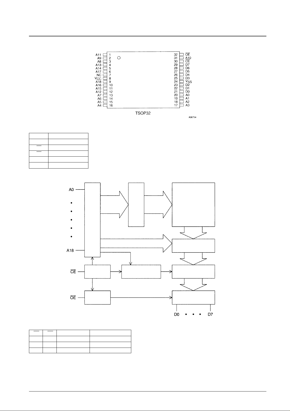
Pin Assignment
No. 5610-2/4
LC374500ST
Block Diagram
Pin Functions
A0 to A18 Address input
Do to D7 Data output
CE Chip enable input
OE Output enable input
V
CC
Power supply
V
SS
Ground
Address buffer
Row decoder
Memory cell array
Column decoder
Sense amplifiers
Output buffer
CE buffer
OE buffer
Internal timing
generator
Function Logic Table
Note: “X” indicates either a high or a low level.
CE OE Output pin state Supply current
H X High-impedance Standby mode current
L H High-impedance Operating mode current
L L DOUT Operating mode current
Top view
Page 3

No. 5610-3/4
LC374500ST
Parameter Symbol Condition Rating Unit Note
Supply voltage V
CC
–0.3 to +7.0 V 1
Input pin voltage V
IN
–0.3 to VCC+ 0.3 V 1, 2
Output pin voltage V
OUT
–0.3 to VCC+ 0.3 V 1
Allowable power dissipation Pd max Ta = 25°C, reference value for the Sanyo DIP. 1.0 W 1
Operating temperature Topr –10 to +70 °C 1
Storage temperature Tstg –55 to +125 °C 1
Specifications
Absolute Maximum Ratings
Note: 1. This device may be permanently damaged by stresses in excess of those listed in the maximum ratings. These are stress ratings only, and
functional operation of the device at these conditions or any other conditions beyond those listed in the “DC Allowable Operating Ranges” item is
not implied.
2. The minimum value is –3.0 V for pulse widths of under 30 ns.
Note: 3. These parameters are sampled, and are not measured for every unit.
Note: Values in parentheses are guaranteed at Ta = 25°C.
Note: Values in parentheses are for V
CC
= 4.5 to 5.5 V
*: t
OD
is defined as the time between the rise of either CE or OE, whichever comes first, and the point when the output goes to the high-impedance
state.
These parameters are sampled, and are not measured for every unit.
Parameter Symbol Conditions
Ratings
Unit Note
min typ max
Input pin capacitance C
IN
VIN= 0 V, reference value for the Sanyo DIP. 8 pF 3
Output pin capacitance C
OUTVOUT
= 0 V, reference value for the Sanyo DIP. 10 pF 3
Capacitance Characteristics at Ta = 25°C, f = 1.0 MHz
Parameter Symbol Conditions
Ratings
Unit
min typ max
Supply voltage V
CC
2.6 5.0 5.5 V
Input high-level voltage V
IH
2.2 VCC+ 0.3 V
Input low-level voltage V
IL
–0.3 +0.6 V
DC Allowable Operating Ranges at Ta = –10 to +70°C, VCC= 2.6 to 5.5 V
Parameter Symbol Conditions
Ratings
Unit
min typ max
Operating current
I
CCA1
CE = 0.2 V, VI= VCC– 0.2 V/0.2 V 30 µA
I
CCA2
CE = VIL, IO= 0 mA, VL= VIH/VIL, f = 10 MHz 55 mA
Standby current
I
CCS1
CE = VCC– 0.2 V 30 (1.0) µA
I
CCS2
CE = V
IH
1.0 (300) mA (µA)
Input leakage current I
LI
VIN= 0 to V
CC
±1.0 µA
Output leakage current I
LO
CE or OE = VIH, V
OUT
= 0 to V
CC
±1.0 µA
Output high-level voltage V
OHIOH
= –0.5 mA 0.8 V
CC
V
Output low-level voltage V
OLIOL
= 0.5 mA 0.2 V
DC Electrical Characteristics at Ta = –10 to +70°C, VCC= 2.6 to 5.5 V
Parameter Symbol Conditions
Ratings
Unit
min typ max
Cycle time t
CYC
200 ns
Address access time t
AA
200 (120) ns
CE access time t
CA
200 (100) ns
OE access time t
OA
80 (40) ns
Output hold time t
OH
20 ns
Output disable time* t
OD
100 ns
AC Characteristics at Ta = –10 to +70°C, VCC= 2.6 to 5.5 V
Page 4

PS No. 5610-4/4
LC374500ST
This catalog provides information as of April, 1998. Specifications and information herein are subject to change
without notice.
■ No products described or contained herein are intended for use in surgical implants, life-support systems, aerospace
equipment, nuclear power control systems, vehicles, disaster/crime-prevention equipment and the like, the failure of
which may directly or indirectly cause injury, death or property loss.
■ Anyone purchasing any products described or contained herein for an above-mentioned use shall:
➀ Accept full responsibility and indemnify and defend SANYO ELECTRIC CO., LTD., its affiliates, subsidiaries and
distributors and all their officers and employees, jointly and severally, against any and all claims and litigation and all
damages, cost and expenses associated with such use:
➁ Not impose any responsibility for any fault or negligence which may be cited in any such claim or litigation on
SANYO ELECTRIC CO., LTD., its affiliates, subsidiaries and distributors or any of their officers and employees
jointly or severally.
■ Information (including circuit diagrams and circuit parameters) herein is for example only; it is not guaranteed for
volume production. SANYO believes information herein is accurate and reliable, but no guarantees are made or implied
regarding its use or any infringements of intellectual property rights or other rights of third parties.
Test Conditions
Input voltage amplitude 0.4 V to 2.8 V
Rise/fall time 5 ns
Input discrimination level 1.5 V
Output discrimination level 1.5 V
Output capacitance See figure 1
*: Includes the oscilloscope and jig capacitances.
Address input
Valid Address
Valid data
Data output
High impedance
Figure 1 Output Load Circuit
Timing Waveforms
Notes on System Design
This LSI adopts the ATD technique, in which operation starts when a change in either the CE or address inputs is
detected. This means that the output data immediately after power is applied is invalid. When using this LSI as program
memory for Z80 and similar microprocessors, applications must take into account the fact that valid data will not be
output after power is first applied unless the value of either the CE or at least one of the address lines is changed after the
power supply has stabilized.
Another point due to the use of the ATD technique is that this LSI is sensitive to input noise. Do not apply voltages
outside the allowable DC input levels for extended periods and do not apply input voltages with large noise components.
 Loading...