

Datasheet LC36256AMLL-70, LC36256AMLL-12, LC36256ALL-85, LC36256ALL-70, LC36256ALL-12 Datasheet (SANYO)
...Page 1
Ordering number : EN4327A
32896HA (OT)/21593JN (OT) No. 4327-1/7
Overview
The LC36256ALL, AMLL are fully asynchronous silicon
gate CMOS static RAMs with a 32768 words × 8 bits
configuration.
This series has CE chip enable pin for device
select/nonselect control and an OE output enable pin for
output control, and features high speed as well as low
power dissipation.
Current dissipation is notably reduced during stand-by and
data retention. For these reasons, this series is most suited
for use in systems requiring high speed, low power
consumption and long-term battery backup. Simple
memory capacity expansion is also supported.
Features
• Access time
70 ns (max.) :
LC36256ALL-70, LC36256AMLL-70
85 ns (max.) :
LC36256ALL-85, LC36256AMLL-85
100 ns (max.) :
LC36256ALL-10, LC36256AMLL-10
120 ns (max.) :
LC36256ALL-12, LC36256AMLL-12
• Low current dissipation
During standby
0.5 µA (max.) / Ta = 25°C
1 µA (max.) / Ta = 0 to +40°C
5 µA (max.) / Ta = 0 to +70°C
During data retention
0.3 µA (max.) / Ta = 25°C
0.6 µA (max.) / Ta = 0 to +40°C
3 µA (max.) / Ta = 0 to +70°C
During operation (DC)
10 mA (max.)
• Single 5 V power supply: 5 V ±10%
• Data retention power supply voltage: 2.0 to 5.5 V
• No clock required (Fully static memory)
• All input/output levels are TTL compatible
• Common input/output pins, with three output states
• Packages
DIP 28- pin (600 mil) plastic package : LC36256ALL
SOP 28-pin (450 mil) plastic package :
LC36256AMLL
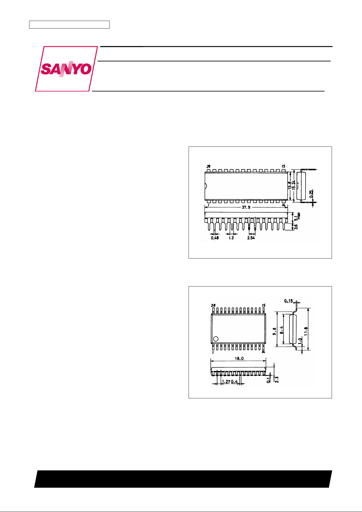
Package Dimensions
unit: mm
3012A-DIP28
unit: mm
3187-SOP28D
SANYO: DIP28
[LC36256ALL]
SANYO: SOP28D
[LC36256AMLL]
LC36256ALL, AMLL-70/85/10/12
SANYO Electric Co.,Ltd. Semiconductor Bussiness Headquarters
TOKYO OFFICE Tokyo Bldg., 1-10, 1 Chome, Ueno, Taito-ku, TOKYO, 110-0005 JAPAN
256 K (32768 words × 8 bits) SRAM
Asynchronous Silicon Gate CMOS LSI
Page 2
LC36256ALL, AMLL-70/85/10/12
No. 4327-2/7
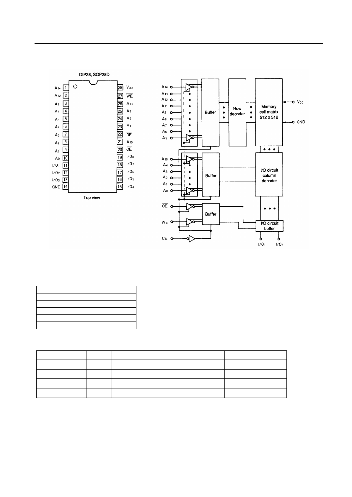
Pin Assignment Block Diagram
Functions
Mode CE OE WE I/O Supply current
Read cycle L L H Data output I
CCA
Write cycle L X L Data input I
CCA
Output disable L H H High impedance I
CCA
Nonselect H X X High impedance I
CCS
X : H or L
Pin Functions
A0 to A14 Address input
WE Read/write control input
OE Output enable input
CE Chip enable input
I/O1 to I/O8 Data input/output
VCC, GND Power supply pins
Page 3
Specifications
Absolute Maximum Ratings at Ta=25°C
Parameter Symbol Conditions Ratings Unit
Maximum supply voltage V
CC max 7.0 V
Input pin voltage V
IN –0.5* to VCC+0.5 V
I/O pin voltage V
I/O –0.5* to VCC+0.5 V
Allowable power dissipation Pd max
LC36256ALL 1.0 W
LC36256AMLL 0.7 W
Operating temperature range Topr 0 to +70 °C
Storage temperature range Tstg –55 to +150 °C
* –3.0 V when pulse width is less than 50 ns
DC Recommended Operating Ranges at Ta = 0 to +70°C
Parameter Symbol min typ max Unit
Power supply voltage V
CC 4.5* 5.0 5.5 V
Input high level voltage V
IH 2.2* VCC+0.3 V
Input low level voltage V
IL –0.3* +0.8 V
* –3.0 V when pulse width is less than 50 ns
DC Electrical Characteristics at Ta = 0 to +70°C, VCC = 5 V ±10%
Parameter Symbol Conditions min typ* max Unit
Input leakage current I
LI VIN = 0 to VCC –0.5 +0.5 µA
I/O leakage current I
LO VCE = VIH or VOE = VIH, –0.5 +0.5 µA
V
I/O = 0 to VCC
Output high level voltage
VOH IOH = –1.0mA 2.4 V
Output low level voltage VOL IOL = 2.1mA 0.4 V
Operating supply
I
CCA1
VCE ≤ 0.2V, 1 5 mA
current (DC)
V
IN ≤ 0.2V or VIN ≥ VCC–0.2V
I
CCA2 VCE = VIL, II/O=0mA 3 10 mA
min cycle
70ns 30 50
Average operating
I
CCA3 Duty = 100%
85ns 25 50
mA
supply current
I
I/O
= 0mA
100ns 23 50
120ns 20 50
0 to +70°C
5
Standby supply
I
CCS1 V
CE ≥VCC
-0.2V
0 to +40°C
1 µA
current
25°C 0.2 0.5
I
CCS2 VCE = VIH 0.4 2 mA
* Reference values at V
CC = 5 V, Ta = 25°C
LC36256ALL, AMLL-70/85/10/12
No. 4327-3/7
Access
time
Page 4

LC36256ALL, AMLL-70/85/10/12
No. 4327-4/7
Input/Output Capacitance at Ta = 25°C, f = 1 MHz
Parameter Symbol Conditions min typ max Unit
Input/output capacitance C
I/O VI/O = 0V 8 pF
Input capacitance C
IN VIN = 0V 6 pF
Note: These parameters were obtained through sampling, and not full-lot measurement.
AC Electrical Characteristics at Ta = 0 to +70°C, VCC= 5 V ±10%
AC testing conditions
Input pulse voltage level : 0.8 V, 2.2 V
Input rise and fall time : 5 ns
Input - output timing level : 1.5 V
Output load : 1 TTL gate + CL = 100 pF (85 ns/100 ns/120 ns)
1 TTL gate + CL = 30 pF (70 ns)
(including scope and jig capacitance)
Read Cycle
Parameter
Symbol
LC36256ALL, AMLL
-70 -85 -10 -12 Unit
min max min max min max min max
Read cycle time t
RC
70 85 100 120 ns
Address access time
t
AA
70 85 100 120 ns
CE access time t
CA
70 85 100 120 ns
OE access time t
OA
35 45 50 60 ns
Output hold time t
OH
20 20 20 20 ns
CE output enable time
t
COE
10 10 10 10 ns
OE output enable time
t
OOE
5 5 5 5 ns
OE output disable time
t
COD
0 30 0 30 0 30 0 30 ns
OE output disable time
t
OOD
0 30 0 30 0 30 0 30 ns
Write Cycle
LC36256ALL, AMLL
Parameter -70 -85 -10 -12 Unit
min max min max min max min max
Write cycle time t
WC
70 85 100 120 ns
Address valid to end of write
t
AW
65 75 80 100 ns
Address setup time t
AS
0 0 0 0 ns
Write pulse width t
WP
50 50 60 70 ns
CE setup time t
CW
65 75 80 100 ns
Write recovery time (WE)
t
WR
0 0 0 0 ns
Write recovery time (CE)
t
WR
1 0 0 0 0 ns
Data setup time t
DS
30 30 35 40 ns
Data hold time t
DH
0 0 0 0 ns
WE output enable time
t
WOE
10 10 10 10 ns
WE output disable time
t
WOD
0 25 0 25 0 25 0 25 ns
Page 5

LC36256ALL, AMLL-70/85/10/12
No. 4327-5/7
Timing Chart
• Read Cycle (1): CE = OE = VIL, WE = VIH
• Read Cycle (2): WE = VIH
• Write Cycle (1): WE Control Note (6)
Page 6

LC36256ALL, AMLL-70/85/10/12
No. 4327-6/7
• Write Cycle (2): CE Control Note (6)
Notes (1) t
COD
, t
OOD
, and t
WOD
are defined as the time at which the outputs becomes the high impedance state and
are not referred to output voltage levels.
(2) An external antiphase signal must not be applied when DOUT is in the output state.
(3) tWPis the time interval that CE and WE are low-level and is defined as the interval from the falling of WE
to the rising of CE or WE whichever is earlier.
(4) tCWis the time interval that CE and WE are low-level and is defined as the time from the falling of CE to
the rising of CE or WE whichever is earlier.
(5) DOUT goes to the high-impedance state when either OE is high-level, CE is high-level, or WE is low-level.
(6) When OE is high-level during the write cycle, DOUT goes to the high-impedance state.
Data Retention Characteristics at Ta = 0 to +70°C
Parameter Symbol Conditions min typ* max Unit
Data retention supply voltage
VDR VCE ≥ VCC–0.2V 2.0 5.5 V
V
CC = 3.0V,
0 to +70°C 3
I
CCDR1
VCE ≥ 2.8V
0 to +40°C 0.6 µA
Data retention supply current
25°C 0.1 0.3
ICCDR2
VCC = 2.0 to 5.5V,
V
CE ≥ VCC–0.2V
0.2 5 µA
CE setup time t
CDR
0 ns
CE hold time t
R
t
RC**
ns
* Reference values at V
CC = 5V, Ta = 25°C ** t
RC
= Read Cycle time
Data Retention Waveform
Page 7

LC36256ALL, AMLL-70/85/10/12
PS No. 4327-7/7
This catalog provides information as of March, 1996. Specifications and information herein are subject to
change without notice.
■ No products described or contained herein are intended for use in surgical implants, life-support systems, aerospace
equipment, nuclear power control systems, vehicles, disaster/crime-prevention equipment and the like, the failure of
which may directly or indirectly cause injury, death or property loss.
■ Anyone purchasing any products described or contained herein for an above-mentioned use shall:
➀ Accept full responsibility and indemnify and defend SANYO ELECTRIC CO., LTD., its affiliates, subsidiaries and
distributors and all their officers and employees, jointly and severally, against any and all claims and litigation and all
damages, cost and expenses associated with such use:
➁ Not impose any responsibility for any fault or negligence which may be cited in any such claim or litigation on
SANYO ELECTRIC CO., LTD., its affiliates, subsidiaries and distributors or any of their officers and employees
jointly or severally.
■ Information (including circuit diagrams and circuit parameters) herein is for example only; it is not guaranteed for
volume production. SANYO believes information herein is accurate and reliable, but no guarantees are made or implied
regarding its use or any infringements of intellectual property rights or other rights of third parties.
 Loading...