

Page 1
Ordering number : ENN*7056
41902RM (OT) No. 7056-1/9
Overview
The LC35V1000BM and LC35V1000BTS-70U are
asynchronous silicon gate CMOS static RAM devices with
a 131,072-word by 8-bit structure. They provide two chip
enable pins (CE1 and CE2) for device select/deselect
control and one output enable pin (OE) for output control.
They feature high speed, low power, and a wide operating
temperature range.This makes them optimal for use in
systems that require high speed, low power, and battery
backup. They also support easy memory expansion.
Features
• Low-voltage operation: 3.0 to 3.6 V
• Wide operating temperature range: –40 to +85°C
• Access time: 70 ns (maximum): LC35V1000BM and
LC35V1000BTS-70U.
• Low current drain
Standby mode: 0.05 µA (typical*) at Ta = +25°C *:
When VCC= 3.0 V
10.0 µA (maximum) at Ta = +70°C
20.0 µA (maximum) at Ta = +85°C
• Data retention voltage: 2.0 to 3.6 V
• No clock required (fully static circuits)
• Input/output shared function pins, 3-state output pins
• Package
32-pin SOP (525 mil) plastic package:
LC35V1000BM
32-pin TSOP (8 ×14 mm) plastic package:
LC35V1000BTS
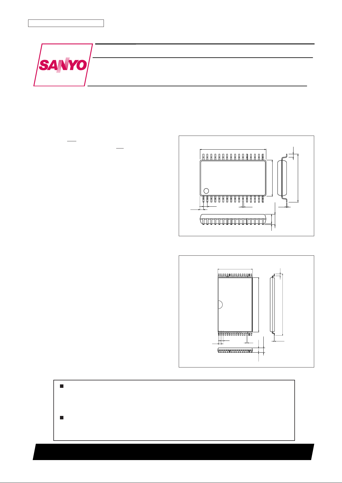
Package Dimensions
unit: mm
3205A-SOP32
unit: mm
3228A-TSOP32DA
1
0.2
3.1max
14.0
0.8
16
17
32
20.5
11.2
0.4
1.27
0.15
(0.73)
(2.7)
Preliminary
SANYO: SOP32
[LC35V1000BM-70U]
0.5
1
16
32 17
1.2max
8.0
0.08
12.4
14.0
0.5
0.2
0.125
(0.25)
(1.0)
SANYO: TSOP32DA
[LC35V1000BTS-70U]
LC35V1000BM, BTS-70U
SANYO Electric Co.,Ltd. Semiconductor Company
TOKYO OFFICE Tokyo Bldg., 1-10, 1 Chome, Ueno, Taito-ku, TOKYO, 110-8534 JAPAN
Asynchronous Silicon Gate
1M (131,072 words
×8 bits) SRAM
CMOS IC
Any and all SANYO products described or contained herein do not have specifications that can handle
applications that require extremely high levels of reliability, such as life-support systems, aircraft’s
control systems, or other applications whose failure can be reasonably expected to result in serious
physical and/or material damage. Consult with your SANYO representative nearest you before using
any SANYO products described or contained herein in such applications.
SANYO assumes no responsibility for equipment failures that result from using products at values that
exceed, even momentarily, rated values (such as maximum ratings, operating condition ranges, or other
parameters) listed in products specifications of any and all SANYO products described or contained
herein.
Page 2
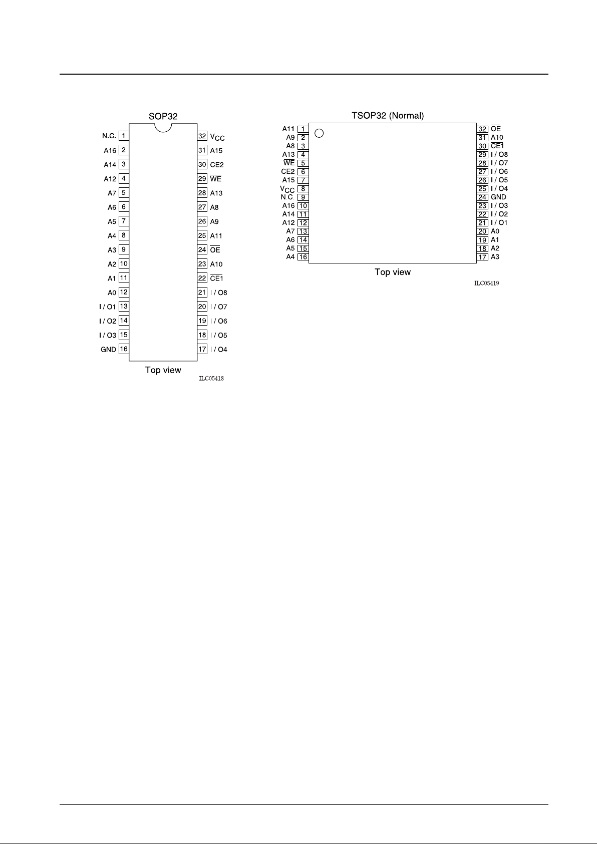
Pin Assignment
No. 7056-2/9
LC35V1000BM, BTS-70U
Page 3
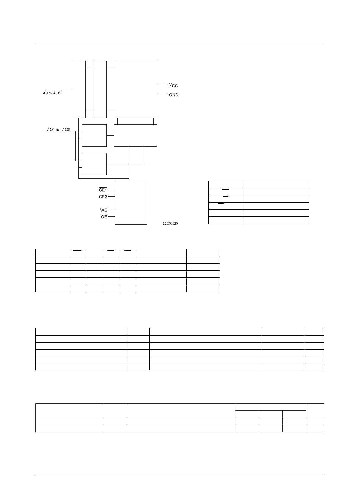
Block Diagram
No. 7056-3/9
LC35V1000BM, BTS-70U
Control
circuit
Data control circuit
Output
buffer
Input
data
buffer
Memory cell array
Raw Decoder
Address buffer
Pin Functions
A0 to A16 Address input
WE Ready/write control input
OE Output enable input
CE, CE2 Chip enable input
I/O1 to I/O8 Data I/O
V
CC
, GND Power supply, ground
Function Table
Note: X indicates H or L.
*: For pulse widths under 30 ns: –2.0 V
Note: This chip may be destroyed if any stress in excess of the absolute maximum ratings is applied.
Note: These parameters are not measured for all devices, but are sampled values.
Mode CE1 CE2 OE WE I/O Supply current
Ready cycle L H L H Data output I
CCA
Write cycle L H X L Data input I
CCA
Output disable L H H H High impedance I
CCA
Unselected
H X X X High impedance I
CCS
X L X X High impedance I
CCS
Parameter Symbol Conditions Ratings Unit
Maximum supply voltage V
CC
max 4.6 V
Input pin voltage V
IN
–0.3* to VCC+ 0.3 V
I/O pin voltage V
I/O
–0.3 to VCC+ 0.3 V
Operating temperature Topr –40 to +85 °C
Storage temperature Tstg –55 to +125 °C
Specifications
Maximum Ratings at Ta = 25°C
Parameter Symbol Conditions
Ratings
Unit
min typ max
Input capacitance C
IN
VIN= 0 V 6 10 pF
I/O capacitance C
I/OVI/O
= 0 V 6 10 pF
I/O Capacitances at Ta = 25°C, f = 1 MHz
Page 4

No. 7056-4/9
LC35V1000BM, BTS-70U
Parameter Symbol Conditions
Ratings
Unit
min typ max
Supply volgate V
CC
3.0 3.3 3.6 V
High-level input voltage V
IH
0.8V
CC
VCC+ 0.3 V
Low-level input voltage V
IL
–0.3* 0.2V
CC
V
DC Allowable Operating Range at Ta = –40 to +85°C
Note: * The minimum value is –2.0 V for pulse width under 30 ns.
Note: * Reference values when V
CC
= 3.0 V and Ta = 25°C.
Parameter Symbol Conditions
Ratings
Unit
min typ max
Input leakage current I
LI
VIN= 0 to V
CC
–1.0 +1.0 µA
I/O leakage current I
LO
V
CE1
= VIHor V
CE2
= VILor VOE= VIHor
–1.0 +1.0 µA
V
WE
= VIL, V
I/O
= 0 to V
CC
Outpu high-level voltage
V
OH1VOH1
= –2.0 mA VCC– 0.4 V
V
OH2VOH2
= –100 µA VCC– 0.1 V
Outpu low-level voltage
V
OL1VOL1
= 2.0 mA 0.4 V
V
OL2VOL2
= –100 µA 0.1 V
Operating supply current I
CCA2VCE1
= VIL, V
CE2
= VIH, I
I/O
= 0 mA, VIN= VIHor V
IL
1.2 mA
(CMOS inputs)
I
CCA3
V
CE1
= VIL, V
CE2
= VIH, min cycle 25
mA
I
I/O
= 0 mA, VIN= VIHor VIL, DUTY100% 1 µs cycle 2
Standby mode supply current V
CE2
≤ 0.2 V or Ta ≤85°C 20
(V
CC
– 0.2 V/0.2 V inputs) I
CCS1(VCE1
≥ VCC– 0.2 V, Ta ≤ 70°C 10 µA
V
CE2
≥ VCC– 0.2 V) Ta ≤ 25°C 0.05
(CMOS inputs) I
CCS2VCE1
= VIHor V
CE2
= VIL, VIN= 0 to V
CC
0.4 mA
DC Electrical Characteristics at Ta = –40 to +85°C, VCC= 3.0 to 3.6 V
Page 5

AC Electrical Characteristics at Ta = –40 to +85°C, VCC= 3.0 to 3.6 V
AC test conditions
Input pulse voltage levels: VIL= 0.2 VCC, VIH= 0.8 V
CC
Input rise and fall times: 5 ns
Input and output timing leves: 0.5 V
CC
Output load: 30 pF (including the jig capacitance)
No. 7056-5/9
LC35V1000BM, BTS-70U
Read cycle
Parameter Symbol min max Unit
Read cyle time t
RC
70 ns
Address access time t
AA
70 ns
CE1 access time t
CA1
70 ns
CE2 access time t
CA2
70 ns
OE access time t
OA
40 ns
Output hold time t
OH
10 ns
CE1 output enable time t
COE1
5 ns
CE2 output enable time t
COE2
5 ns
OE output enable time t
OCE
0 ns
CE1 output disable time t
COD1
35 ns
CE2 output disable time t
COD2
35 ns
OE output disable time t
OOD
30 ns
Write cycle
Parameter Symbol min max Unit
Write cyle time t
WC
70 ns
Address setup time t
AS
0 ns
Write pulse width tWP 50 ns
CE1 setup time t
CW1
60 ns
CE2 setup time t
CW2
60 ns
Write recovery time t
WR
0 ns
OE1 write recovery time t
WR1
0 ns
CE2 write recovery time t
WR2
0 ns
Data setup time t
DS
40 ns
Data hold time t
DH
0 ns
OE1 data hold time t
DH1
0 ns
CE2 data hold time t
DH2
0 ns
WE output enable time t
WOE
5 ns
WE output disable time t
WOD
35 ns
Page 6

Timing Charts
Read cycle (1)
Write cycle (1) (WE write)
No. 7056-6/9
LC35V1000BM, BTS-70U
*5
*5
*2*2
*7
*3
*4
*4
Page 7

No. 7056-7/9
LC35V1000BM, BTS-70U
Write cycle (2) (CE1 write)
*5
*4
*4
*3
Write cycle (2) (CE2 write)
*5
*4
*4
*3
Page 8

Notes: 1. The times t
COD1
, t
COD2
, t
OOD
, and t
WOD
are stipulated as the times until the output reaches the high-impedance
state. They are not stipulated by output voltage level.
2. Do not apply reverse phase signals to the data outputs when the data outputs are in the output state.
3. tWPis the period that CE1 and WE are at the low level and CE2 is at the high level, and is defined as the time
from the fall of WE until the rise of CE1 or WE or the fall of CE2, whichever occurs first.
4. t
CW1
and t
CW2
are the period that CE1 and WE are at the low level and CE2 is at the high level, and are defined
as the time from the fall of CE1 or the rise of CE2 to the rise of either CE1 or WE or the fall of CE2, whichever
occurs first.
5. The data outputs go to the high-impedance state when any one of the following states hold: OE is at the high
level, CE1 is at the high level, CE2 is at the low level, or WE is at the low level.
6. If OE is at the high level during the write cycle, the data outputs will go to the high-impedance state.
No. 7056-8/9
LC35V1000BM, BTS-70U
Parameter Symbol Conditions
Ratings
Unit
min typ max
Data retention supply voltage
V
DR1VCE1
≥ VCC– 0.2 V, V
CE2
≥ VCC– 0.2 V or V
CE2
≤ 0.2 V 2.0 3.6 V
V
DR2VCE2
≤ 0.2 V 2.0 3.6 V
V
CC
= 3.0 V, V
CE1
≥ VCC– 0.2 V, –40°C to +85°C 16
Data retention supply current I
CCDR1VCE2
≥ VCC– 0.2 V, –40°C to +70°C 8 µA
or V
CE2
≤ 0.2 V +25°C 0.05
Chip enable setup time t
CDR
0 ns
Chip enable hold time t
R
5 ms
Data Retention Characteristics at Ta = –40 to +85°C
Data Retention Waveforms (1) (CE1 control)
Note: * Ta = +25°C
Data retention mode
Data Retention Waveforms (2) (CE2 control)
Data retention mode
Page 9

PS No. 7056-9/9
LC35V1000BM, BTS-70U
This catalog provides information as of April, 2002. Specifications and information herein are subject to
change without notice.
Specifications of any and all SANYO products described or contained herein stipulate the performance,
characteristics, and functions of the described products in the independent state, and are not guarantees
of the performance, characteristics, and functions of the described products as mounted in the customer’s
products or equipment. To verify symptoms and states that cannot be evaluated in an independent device,
the customer should always evaluate and test devices mounted in the customer’s products or equipment.
SANYO Electric Co., Ltd. strives to supply high-quality high-reliability products. However, any and all
semiconductor products fail with some probability. It is possible that these probabilistic failures could
give rise to accidents or events that could endanger human lives, that could give rise to smoke or fire,
or that could cause damage to other property. When designing equipment, adopt safety measures so
that these kinds of accidents or events cannot occur. Such measures include but are not limited to protective
circuits and error prevention circuits for safe design, redundant design, and structural design.
In the event that any or all SANYO products (including technical data, services) described or contained
herein are controlled under any of applicable local export control laws and regulations, such products must
not be exported without obtaining the export license from the authorities concerned in accordance with the
above law.
No part of this publication may be reproduced or transmitted in any form or by any means, electronic or
mechanical, including photocopying and recording, or any information storage or retrieval system,
or otherwise, without the prior written permission of SANYO Electric Co., Ltd.
Any and all information described or contained herein are subject to change without notice due to
product/technology improvement, etc. When designing equipment, refer to the “Delivery Specification”
for the SANYO product that you intend to use.
Information (including circuit diagrams and circuit parameters) herein is for example only; it is not
guaranteed for volume production. SANYO believes information herein is accurate and reliable, but
no guarantees are made or implied regarding its use or any infringements of intellectual property rights
or other rights of third parties.
 Loading...