

Datasheet LC35256D-10, LC35256DT-10, LC35256DM-70, LC35256DM-10, LC35256DT-70 Datasheet (SANYO)
Page 1

Overview
The LC35256D, LC35256DM, and LC35256DT are
32768-word × 8-bit asynchronous silicon gate CMOS
static RAMs. These devices use a 6-transistor full CMOS
memory cell, and feature low-voltage operation, low
current drain, and an ultralow standby current. They
provide two control signal inputs: an OE input for highspeed access and a chip select (CE) input for device
selection and low power operating mode. This makes
these devices optimal for systems that require low power
or battery backup, and they allow memory to be expanded
easily. Their ultralow standby current allows capacitorbased backup to be used as well. Since they support 3-V
operation, they are appropriate for use in portable systems
that operate from batteries.
Features
• Supply voltage range:2.7 to 5.5 V
— 5-V operation: 5.0 V±10%
— 3-V operation: 2.7 to 3.6 V
• Access times
— 5-V operation
LC35256DM, DT-70: 70 ns (max)
LC35256D, DM, DT-10: 100 ns (max)
— 3-V operation
LC35256DM, DT-70: 200 ns (max)
LC35256D, DM, DT-10: 500 ns (max)
• Standby current
— 5-V operation: 1.0 µA (Ta ≤ 60°C),
5.0 µA (Ta ≤ 85°C)
— 3-V operation: 0.8 µA (Ta ≤ 60°C),
4.0 µA (Ta ≤ 85°C)
• Operating temperature range: –40 to +85°C
• Data retention supply voltage: 2.0 to 5.5 V
• All I/O levels
— 5-V operation: TTL compatible
— 3-V operation: VCC– 0.2 V/0.2 V
• Shared I/O pins and 3-state outputs
• No clock signal required.
• Packages
— 28-pin DIP (600 mil) plastic package: LC35256D
— 28-pin SOP (450 mil) plastic package: LC35256DM
— 28-pin TSOP (8 × 13.4 mm) plastic package:
LC35256DT
Package Dimensions
unit: mm
3012A-DIP28
unit: mm
3187-SOP28D
unit: mm
3221-TSOP28(type-I)
CMOS IC
51398RM (OT) No. 5823-1/8
SANYO: DIP28
[LC35256D]
SANYO: SOP28D
[LC35256DM]
SANYO: TSOP28(type-I)
[LC35256DT]
SANYO Electric Co.,Ltd. Semiconductor Bussiness Headquarters
TOKYO OFFICE Tokyo Bldg., 1-10, 1 Chome, Ueno, Taito-ku, TOKYO, 110-8534 JAPAN
Dual Control Pins: OE and CE
256K (32768-word × 8-bit) SRAM
LC35256D-10, LC35256DM, DT-70/10
Ordering number : EN5823
Page 2
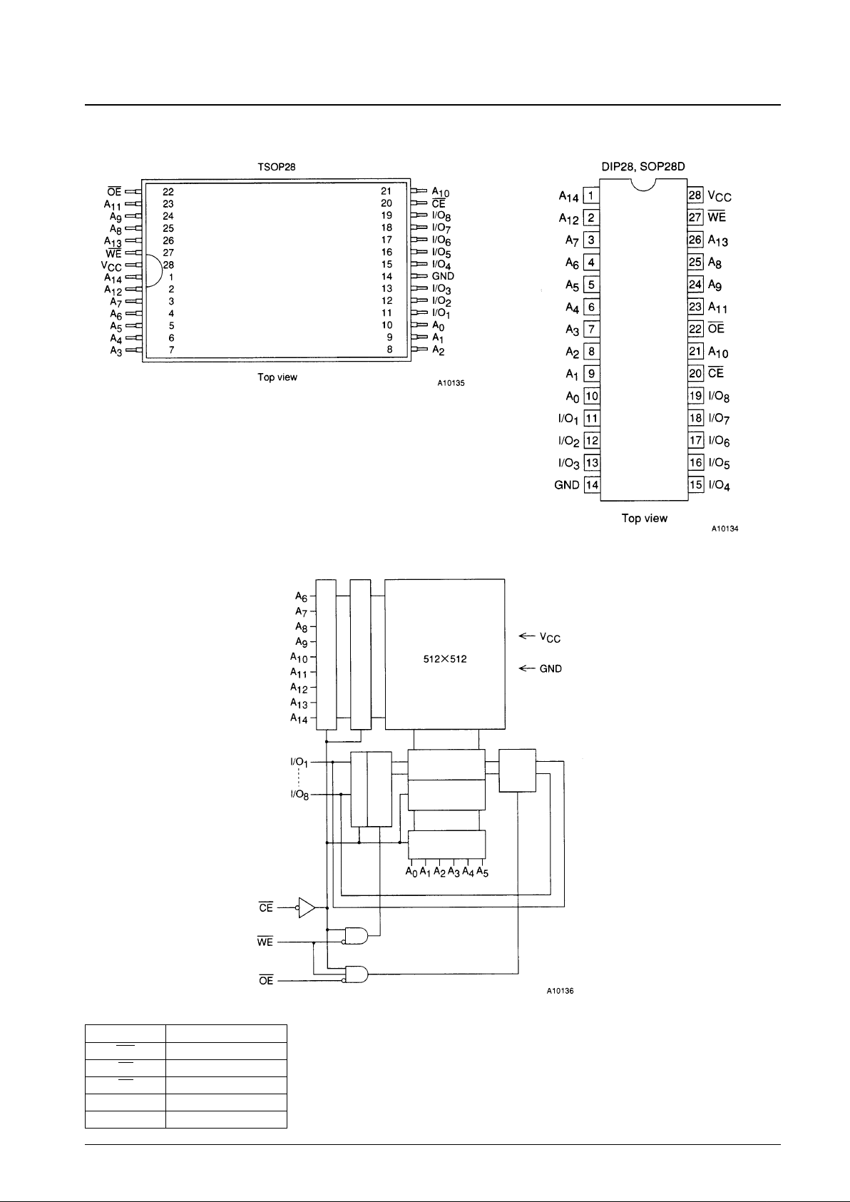
Pin Assignment
No. 5823-2/8
LC35256D-10, LC35256DM, DT-70/10
Block Diagram
Pin Functions
A0 to A14 Address inputs
WE Read/write control input
OE Output enable input
CE Chip enable input
I/O1 to I/O8 Data I/O
V
CC
, GND Power supply, ground
Address buffer
Address buffer
Input data buffer
Input data
control circuit
Row decoder
Memory cell array
Column
I/O circuit
Output
data
buffer
Column
decoder
Page 3
No. 5823-3/8
LC35256D-10, LC35256DM, DT-70/10
Function Table
X : H or L
Note *: –3.0 V for pulse widths of up to 30 ns.
Note: These parameters are not measured in all units, but rather are only measured in sampled units.
Note *: –3.0 V for pulse widths of up to 30 ns.
Note *: Reference value at Ta = 25°C, V
CC
= 5 V.
Mode CE OE WE I/O Supply current
Read cycle L L H Data output I
CCA
Write cycle L X L Data input I
CCA
Output disable L H H High-impedance I
CCA
Unselected H X X High-impedance I
CCS
Parameter Symbol Conditions Ratings Unit
Maximum supply voltage V
CC
max 7.0 V
Input pin voltage V
IN
–0.3* to VCC+ 0.3 V
I/O pin voltage V
I/O
–0.3 to VCC+ 0.3 V
Operating temperature Topr –40 to +85 °C
Storage temperature Tstg –55 to +125 °C
Specifications
Absolute Maximum Ratings
Parameter Symbol Conditions
Ratings
Unit
min typ max
I/O pin capacitance C
I/OVI/O
= 0 V 6 10 pF
Input pin capacitance C
IN
VIN= 0 V 6 10 pF
I/O Capacitances at Ta = 25°C, f = 1 MHz
[5-V Operation]
Parameter Symbol Conditions
Ratings
Unit
min typ max
Supply voltage V
CC
4.5 5.0 5.5 V
Input voltages
V
IH
2.2 VCC+ 0.3 V
V
IL
–0.3* +0.8 V
DC Allowable Operating Ranges at Ta = –40 to +85°C, VCC= 4.5 to 5.5 V
Parameter Symbol Conditions
Ratings
Unit
min typ* max
Input leakage current I
LI
VIN= 0 to V
CC
–1.0 +1.0 µA
Output leakage current I
LO
VCE= VIHor VOE= VIHor VWE= VIL, V
I/O
= 0 to V
CC
–1.0 +1.0 µA
High-level output voltage V
OHIOH
= –1.0 mA 2.4 V
Low-level output voltage V
OLIOL
= 2.0 mA 0.4 V
I
CCA2VCE
= VIL, I
I/O
= 0 mA, VIN= VIHor V
IL
5.0 mA
Operating
TTL inputs V
CE
= VIL, VIN= VIHor VIL,
min LC35256DM, DT-70 35 40 mA
current drain I
CCA3
I
I/O
= 0 mA, Duty 100%
cycle LC35256D, DM, DT-10 25 30 mA
1 µs cycle 3.5 6.0 mA
V
CC
– 0.2 V/ VCE≥ VCC– 0.2 V,
Ta ≤ 25°C 0.01 µA
Standby mode
0.2 V inputs
I
CCS1
VIN= 0 to V
CC
Ta ≤ 60°C 1.0 µA
current drain Ta ≤ 85°C 5.0 µA
TTL inputs I
CCS2VCE
= VIH, VIN= 0 to V
CC
1.0 mA
DC Electrical Characteristics at Ta = –40 to +85°C, VCC= 4.5 to 5.5 V
Page 4

AC Electrical Characteristics at Ta = –40 to +85°C, VCC= 4.5 to 5.5 V
No. 5823-4/8
LC35256D-10, LC35256DM, DT-70/10
LC35256D, DM, DT
Parameter Symbol -70* -10 Unit
min max min max
Read cycle time t
RC
70 100 ns
Address access time t
AA
70 100 ns
CE access time t
CA
70 100 ns
OE access time t
OA
35 50 ns
Output hold time t
OH
10 10 ns
CE output enable time t
COE
10 10 ns
OE output enable time t
OOE
5 5 ns
CE output disable time t
COD
30 30 ns
OE output disable time t
OOD
25 25 ns
Read Cycle
Note *: Specification values for the LC35256DM and LC35256DT.
LC35256D, DM, DT
Parameter Symbol -70* -10 Unit
min max min max
Write cycle time t
WC
70 100 ns
Address setup time t
AS
0 0 ns
Write pulse width t
WP
55 60 ns
CE setup time t
CW
60 70 ns
Write recovery time t
WR
0 0 ns
CE write recovery time t
WR1
0 0 ns
Data setup time t
DS
35 40 ns
Data hold time t
DH
0 0 ns
CE data hold time t
DH1
0 0 ns
WE output enable time t
WOE
5 5 ns
WE output disable time t
WOD
30 30 ns
Write Cycle
Note *: Specification values for the LC35256DM and LC35256DT.
Note *: –2.0 V for pulse widths of up to 30 ns.
[3-V Operation]
Parameter Symbol Conditions
Ratings
Unit
min typ max
Supply voltage V
CC
2.7 3.0 3.6 V
Input voltages
V
IH
VCC– 0.2 VCC+ 0.3 V
V
IL
–0.3* +0.2 V
DC Allowable Operating Ranges at Ta = –40 to +85°C, VCC= 2.7 to 3.6 V
AC test conditions
Input pulse voltage level V
IH
= 2.4 V, VIL= 0.6 V
Input rise and fall times 5 ns
Input and output timing level 1.5 V
Output load
LC35256DM, DT-70 One TTL gate + 30 pF (Including jig capacitances.)
LC35256D, DM, DT-10 One TTL gate + 100 pF (Including jig capacitances.)
Page 5

No. 5823-5/8
LC35256D-10, LC35256DM, DT-70/10
Note *: Reference value at Ta = 25°C, VCC= 3 V.
Parameter Symbol Conditions
Ratings
Unit
min typ* max
Input leakage current I
LI
VIN= 0 to V
CC
–1.0 +1.0 µA
Output leakage current I
LO
VCE= VIHor VOE= VIHor VWE= VIL, V
I/O
= 0 to V
CC
–1.0 +1.0 µA
High-level output voltage V
OHIOH
= –0.5 mA VCC– 0.2 V
Low-level output voltage V
OLIOL
= 1.0 mA 0.2 V
Operating V
CC
– 0.2 V/
V
CE
= VIL, VIN= VIHor VIL,
min LC35256DM, DT-70 7 10 mA
current drain 0.2 V inputs
I
CCA4
I
I/O
= 0 mA, Duty 100%
cycle LC35256D, DM, DT-10 3 5 mA
1 µs cycle 1.5 2.5 mA
Standby mode V
CC
– 0.2 V/ VCE≥ VCC– 0.2 V,
Ta ≤ 25°C 0.01 µA
current drain 0.2 V inputs
I
CCS1
VIN= 0 to V
CC
Ta ≤ 60°C 0.8 µA
Ta ≤ 85°C 4.0 µA
DC Electrical Characteristics at Ta = –40 to +85°C, VCC= 2.7 to 3.6 V
AC Electrical Characteristics at Ta = –40 to +85°C, VCC= 2.7 to 3.6 V
LC35256D, DM, DT
Parameter Symbol -70* -10 Unit
min max min max
Read cycle time t
RC
200 500 ns
Address access time t
AA
200 500 ns
CE access time t
CA
200 500 ns
OE access time t
OA
100 250 ns
Output hold time t
OH
20 20 ns
CE output enable time t
COE
20 20 ns
OE output enable time t
OOE
10 10 ns
CE output disable time t
COD
60 120 ns
OE output disable time t
OOD
50 100 ns
Read Cycle
Note *: Specification values for the LC35256DM and LC35256DT.
AC test conditions
Input pulse voltage level V
IH
= VCC– 0.2 V, VIL= 0.2 V
Input rise and fall times 10 ns
Input and output timing level 1.5 V
Output load
LC35256DM, DT-70 30 pF (Including jig capacitances.)
LC35256D, DM, DT-10 100 pF (Including jig capacitances.)
Page 6

No. 5823-6/8
LC35256D-10, LC35256DM, DT-70/10
LC35256D, DM, DT
Parameter Symbol -70* -10 Unit
min max min max
Write cycle time t
WC
200 500 ns
Address setup time t
AS
0 0 ns
Write pulse width t
WP
140 200 ns
CE setup time t
CW
150 250 ns
Write recovery time t
WR
0 0 ns
CE write recovery time t
WR1
0 0 ns
Data setup time t
DS
130 180 ns
Data hold time t
DH
0 0 ns
CE data hold time t
DH1
0 0 ns
WE output enable time t
WOE
10 10 ns
WE output disable time t
WOD
60 120 ns
Write Cycle
Note *: Specification values for the LC35256DM and LC35256DT.
Timing Charts
Read Cycle *
1
*
5
Page 7

No. 5823-7/8
LC35256D-10, LC35256DM, DT-70/10
Write Cycle 1 (WE write) *
6
Write Cycle 2 (CE write) *
6
Notes: 1. Applications must set WE high during the read cycle.
2. External circuits in the application must not apply reverse phase signals to the D
OUT
pins when those pins are in the output state.
3. The time t
WP
is the period when CE and WE are both low. It is defined as the time from the fall of WE to the rise of CE or the rise of WE, whichever
occurs first.
4. The time t
CW
is the period when CE and WE are both low. It is defined as the time from the fall of CE to the rise of CE or the rise of WE, whichever
occurs first.
5. The data outputs (D
OUT
) go to the high-impedance state if any one of the following conditions hold: OE is high, CE is high, or WE is low.
6. OE must be held either high or low during the write cycle.
7. The D
OUT
pins have the same phase as the write cycle write data.
*
5
*
5
Page 8

PS No. 5823-8/8
LC35256D-10, LC35256DM, DT-70/10
Notes on Circuit Design
Take the following operations into account when designing circuits that use these products to assure that none of the
items in the maximum ratings are exceeded.
• Supply voltage variations and fluctuations
• Manufacturing variations in the electrical characteristics of the electrical components, including semiconductor
devices, resistors, and capacitors.
• Ambient temperature
• Variations and fluctuations in the input and clock signals
• Possible application of abnormal pulses
Parameters listed in the allowable operating ranges must never exceed their stipulated ranges.
If input pins to a CMOS IC are left open, through currents may occur in internal circuits to which intermediate potentials
are input and result in incorrect circuit operation. Always verify that any unused pins are set up in appropriate states.
This catalog provides information as of May, 1998. Specifications and information herein are subject to change
without notice.
■ No products described or contained herein are intended for use in surgical implants, life-support systems, aerospace
equipment, nuclear power control systems, vehicles, disaster/crime-prevention equipment and the like, the failure of
which may directly or indirectly cause injury, death or property loss.
■ Anyone purchasing any products described or contained herein for an above-mentioned use shall:
➀ Accept full responsibility and indemnify and defend SANYO ELECTRIC CO., LTD., its affiliates, subsidiaries and
distributors and all their officers and employees, jointly and severally, against any and all claims and litigation and all
damages, cost and expenses associated with such use:
➁ Not impose any responsibility for any fault or negligence which may be cited in any such claim or litigation on
SANYO ELECTRIC CO., LTD., its affiliates, subsidiaries and distributors or any of their officers and employees
jointly or severally.
■ Information (including circuit diagrams and circuit parameters) herein is for example only; it is not guaranteed for
volume production. SANYO believes information herein is accurate and reliable, but no guarantees are made or implied
regarding its use or any infringements of intellectual property rights or other rights of third parties.
Notes: 1. Reference value at Ta = 25°C, VCC= 3 V.
2. t
RC
: Read cycle time
Parameter Symbol Conditions
Ratings
Unit
min typ*
1
max
Data retention supply voltage V
DRVCE
≥ VCC– 0.2 V 2.0 5.5 V
V
CC
= 3.0 V,
Ta ≤ 25°C 0.01 µA
Data retention current drain I
CCDR
VCE≥ VCC– 0.2 V
Ta ≤ 60°C 0.7 µA
Ta ≤ 85°C 3.5 µA
Chip enable setup time t
CDR
0 ns
Chip enable hold time t
R
tRC*
2
ns
Data Retention Characteristics at Ta = –40 to +85°C
Data Retention Waveforms
Note *: V
CCL
5-V operation: 4.5 V
3-V operation: 2.7 V
Data retention mode
 Loading...