

Page 1
1.2A 1.5MHz 7V Synchronous Buck Converter
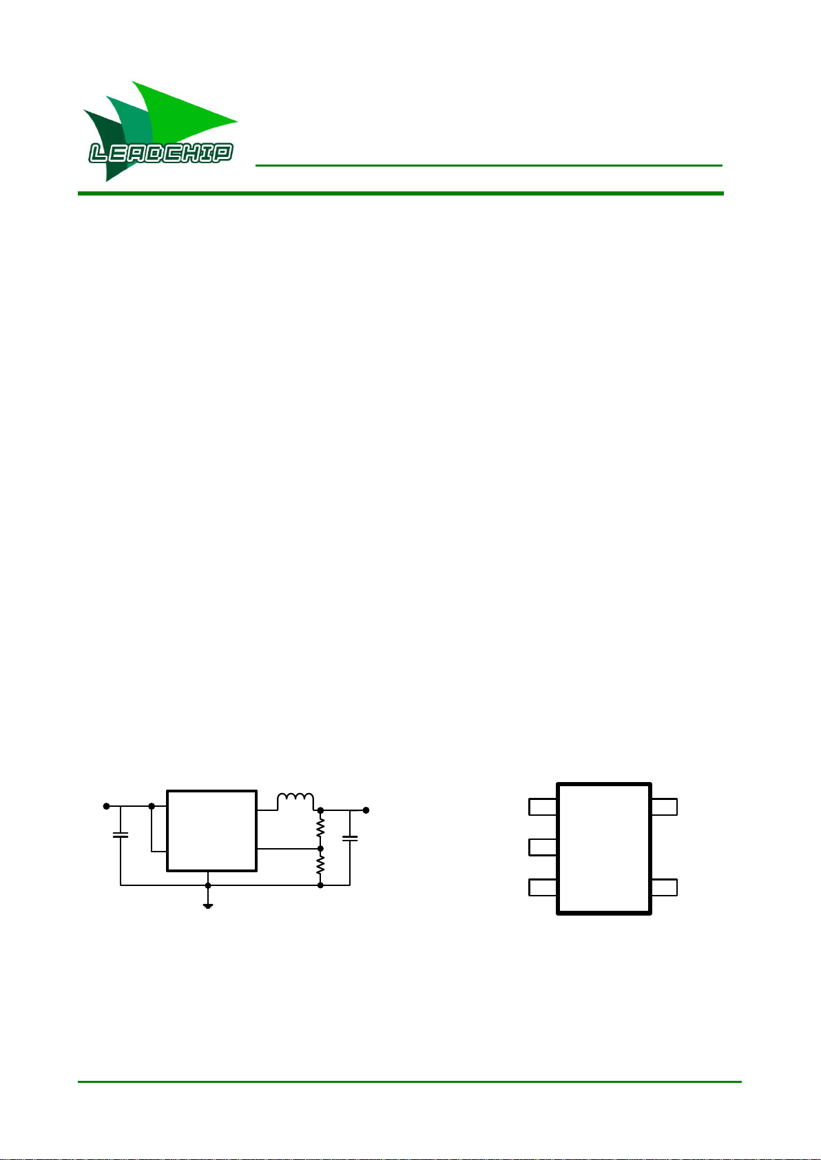
LC3406
GND
FB
IN
SW
240K
120K
10uF
LC3406
10uF
V
OUT
1.8V/1A
VIN
2.6V to 7V
1.8V/1A Step-Down Converter
2.2uH
EN
1
2
3
5
4
SOT23-5
FB
EN
SW
IN
G
GGZZ
DESCRIPTION
The LC3406 is a high-efficiency, DC-to-DC stepdown switching regulators, capable of delivering up
to 1.2A of output current. The device operates from
an input voltage range of 2.6V to 7.0V and provides
an output voltage from 0.6V to VIN, making the
LC3406 ideal for low voltage power conversions.
Running at a fixed frequency of 1.5MHz allows the
use of small external components, such as ceramic
input and output caps, as well as small inductors,
while still providing low output ripples. This low
noise output along with its excellent efficiency
achieved by the internal synchronous rectifier,
making LC3406 an ideal green replacement for large
power consuming linear regulators. Internal softstart control circuitry reduces inrush current. Shortcircuit and thermal-overload protection improves
design reliability.
LC3406 is housed in a SOT23-5 Package
FEATURES
High Efficiency: Up to 96%
Capable of Delivering 1.2A
1.5MHz Switching Frequency
No External Schottky Diode Needed
Low dropout 100% Duty operation
Internal Compensation and Soft-Start
Current Mode control
0.6V Reference for Low Output voltages
Logic Control Shutdown (IQ<1uA)
Thermal shutdown and UVLO
Available in SOT23-5
APPLICATIONS
Cellular phones
Digital Cameras
MP3 and MP4 players
Set top boxes
Wireless and DSL Modems
USB supplied Devices in Notebooks
Portable Devices
TYPICAL APPLICATION
www.leadchip.com 1 Your final power solution
PIN OUT & MARKING
Page 2
LC3406
PART No.
PACKAGE
Tape&Reel
LC3406CB5TR
SOT23-5
3000/Reel
Parameter
Value
Max Input Voltage
7V
Max Operating Junction Temperature(Tj)
125C
Ambient Temperature(Ta)
-40C – 85C
Maximum Power Dissipation
SOT23-5
400mW
Storage Temperature(Ts)
-40C - 150C
Lead Temperature & Time
260C, 10S
ESD (HBM)
>2000V
Parameter
Value
Input Voltage Range
Max. 5.5V
Operating Junction Temperature(Tj)
-20C –125C
Symbol
Parameter
Conditions
Min
Typ
Max
Unit
VDD
Input Voltage Range
2.6 7.0
V
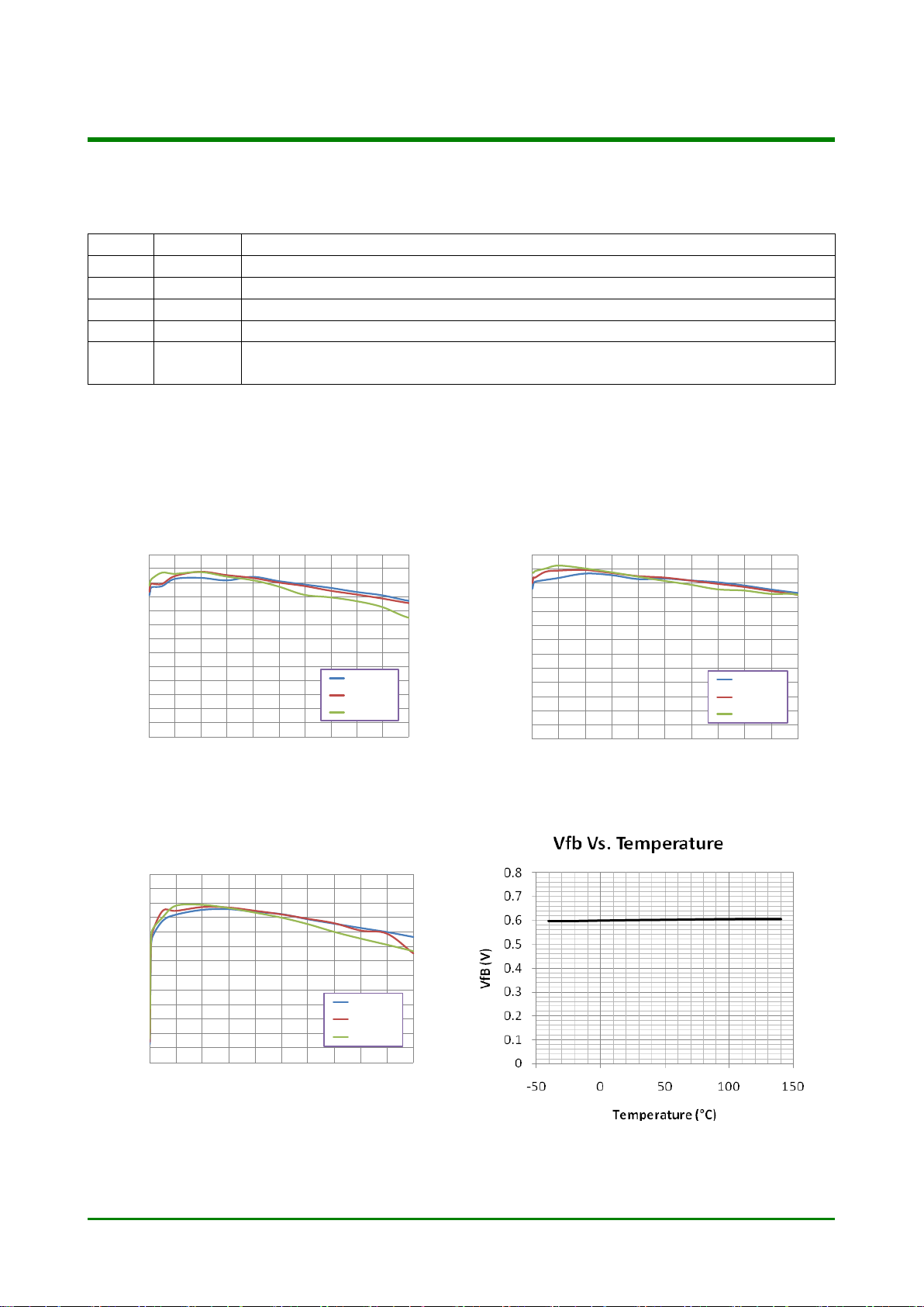
Vref
Feedback Voltage
Vin=5V
0.585
0.6
0.615
V
Ifb
Feedback Leakage current
0.1
0.4
uA
Iq
Quiescent Current
Active, Vfb=0.65, No Switching
35
uA
Shutdown
1
uA
LnReg
Line Regulation
Vin=2.7V to 5.5V
0.04
0.2
%/V
LdReg
Load Regulation
Iout=0.01 to 1A
0.1
0.2
%/A
Fsoc
Switching Frequency
1.5
MHz
RdsonP
PMOS Rdson
300
400
mohm
RdsonN
NMOS Rdson
220
300
mohm
Ilimit
Peak Current Limit
1.2
1.5 2 A
Iswlk
SW Leakage Current
Vout=5.5V, VSW=0 or 5.5V,
EN=0V
10
uA
Ienlk
EN Leakage Current
1
uA
Vh_en
EN Input High Voltage
1.5
V
Vl_en
EN Input Low Voltage
0.4
V
ORDERING INFORMATION
ABSOLUTE MAXIMUM RATING
Note: Exceed these limits to damage to the device. Exposure to absolute maximum rating conditions may affect
device reliability.
RECOMMENDED WORK CONDITIONS
ELECTRICAL CHARACTERISTICS
(VDD=5V, TA=25C)
www.leadchip.com 2 Your final power solution
Page 3
LC3406
PIN #
NAME
DESCRIPTION
1
EN
Enable pin for the IC. Drive the pin to high to enable the part, and low to disable
2
GND
Ground
3
SW
Inductor connection. Connect an inductor between SW and the regulator output.
4
IN
Supply voltage.
5
FB
Feedback input. Connect an external resistor divider from the output to FB and
GND to set the output to a voltage between 0.6V and Vin
35
40
45
50
55
60
65
70
75
80
85
90
95
100
0 100 200 300 400 500 600 700 800 900 1000
Efficiency (%)
Load Current (mA)
Efficiency VS Load Current,
Vout=1.8V
Vin=4.2V
Vin=3.6V
Vin=2.7V
35
40
45
50
55
60
65
70
75
80
85
90
95
100
0 100 200 300 400 500 600 700 800 900 1000
Efficiency (%)
Load Current (mA)
Efficiency VS Load Current,
Vout=2.5V
Vin=4.2V
Vin=3.6V
Vin=2.7V
35
40
45
50
55
60
65
70
75
80
85
90
95
100
0 100 200 300 400 500 600 700 800 900 1000
Efficiency (%)
Load Current (mA)
Efficiency VS Load Current,
Vout=1.2V
Vin=4.2V
Vin=3.6V
Vin=2.7V
PIN DESCRIPTION
ELECTRICAL PERFORMANCE
Tested under TA=25C, unless otherwise specified
www.leadchip.com 3 Your final power solution
Page 4

LC3406
Output Ripple and SW at no load
Vin=5V / Vout=2.5V
Output Ripple and SW at 1A load
Vin=5V / Vout=2.5V
+
-
0.6V Ref
PWM
Logic
Anti-
ShootThrough
Driver
+
-
EA
+
-
+
-
Slope Comp
OSC
Σ
SW
GND
UVLO &
Thermal
shutdown
Vcomp
ISense
Comp
Network
FB
EN
IN
BLOCK DIAGRAM
www.leadchip.com 4 Your final power solution
Page 5

LC3406
DETAILED DESCRIPTION
The LC3406 high-efficiency switching regulator is a
small, simple, DC-to-DC step-down converter
capable of delivering up to 1A of output current.
The device operates in pulse-width modulation
(PWM) at 1.5MHz from a 2.6V to 5.5V input voltage
and provides an output voltage from 0.6V to VIN,
making the LC3406 ideal for on-board postregulation applications. An internal synchronous
rectifier improves efficiency and eliminates the
typical Schottky free-wheeling diode. Using the on
resistance of the internal high-side MOSFET to
sense switching currents eliminates current-sense
resistors, further improving efficiency and cost.
Loop Operation
LC3406 uses a PWM current-mode control scheme.
An open-loop comparator compares the integrated
voltage-feedback signal against the sum of the
amplified current-sense signal and the slope
compensation ramp. At each rising edge of the
internal clock, the internal high-side MOSFET turns
on until the PWM comparator terminates the on
cycle. During this on-time, current ramps up
through the inductor, sourcing current to the
output and storing energy in the inductor. The
current mode feedback system regulates the peak
inductor current as a function of the output voltage
error signal. During the off cycle, the internal highside P-channel MOSFET turns off, and the internal
low-side N-channel MOSFET turns on. The inductor
releases the stored energy as its current ramps
down while still providing current to the output.
Current Sense
An internal current-sense amplifier senses the
current through the high-side MOSFET during on
time and produces a proportional current signal,
which is used to sum with the slope compensation
signal. The summed signal then is compared with
the error amplifier output by the PWM comparator
to terminate the on cycle.
Current Limit
There is a cycle-by-cycle current limit on the highside MOSFET of 1.5A(typ). When the current
flowing out of SW exceeds this limit, the high-side
MOSFET turns off and the synchronous rectifier
turns on. LC3406 utilizes a frequency fold-back
mode to prevent overheating during short-circuit
output conditions. The device enters frequency
fold-back mode when the FB voltage drops below
200mV, limiting the current to 1.5A (typ) and
reducing power dissipation. Normal operation
resumes upon removal of the short-circuit
condition.
Soft-start
LC3406 has a internal soft-start circuitry to reduce
supply inrush current during startup conditions.
When the device exits under-voltage lockout
(UVLO), shutdown mode, or restarts following a
thermal-overload event, the l soft-start circuitry
slowly ramps up current available at SW.
UVLO and Thermal Shutdown
If IN drops below 2.5V, the UVLO circuit inhibits
switching. Once IN rises above 2.6V, the UVLO
clears, and the soft-start sequence activates.
Thermal-overload protection limits total power
dissipation in the device. When the junction
temperature exceeds TJ= +160°C, a thermal sensor
forces the device into shutdown, allowing the die to
cool. The thermal sensor turns the device on again
after the junction temperature cools by 15°C,
resulting in a pulsed output during continuous
overload conditions. Following a thermal-shutdown
condition, the soft-start sequence begins.
Design Procedure
Setting Output Voltages
Output voltages are set by external resistors. The
FB_ threshold is 0.6V.
RTOP = RBOTTOM[(VOUT / 0.6) - 1]
Input Capacitor Selection
The input capacitor in a DC-to-DC converter reduces
current peaks drawn from the battery or other
input power source and reduces switching noise in
the controller. The impedance of the input
capacitor at the switching frequency should be less
than that of the input source so high-frequency
www.leadchip.com 5 Your final power solution
Page 6

LC3406
switching currents do not pass through the input
source. The output capacitor keeps output ripple
small and ensures control-loop stability. The output
capacitor must also have low impedance at the
switching frequency. Ceramic, polymer, and
tantalum capacitors are suitable, with ceramic
exhibiting the lowest ESR and high-frequency
impedance. Output ripple with a ceramic output
capacitor is approximately as follows:
VRIPPLE = IL(PEAK)[1 / (2π x fOSC x COUT)]
If the capacitor has significant ESR, the output
ripple component due to capacitor ESR is as follows:
VRIPPLE(ESR) = IL(PEAK) x ESR
Application Information
Layout is critical to achieve clean and stable
operation. The switching power stage requires
particular attention. Follow these guidelines for
good PC board layout:
1) Place decoupling capacitors as close to the IC as
possible
2) Connect input and output capacitors to the
same power ground node with a star ground
configuration then to IC ground.
3) Keep the high-current paths as short and wide
as possible. Keep the path of switching current
(C1 to IN and C1 to GND) short. Avoid vias in
the switching paths.
4) If possible, connect IN, SW, and GND separately
to a large copper area to help cool the IC to
further improve efficiency and long-term
reliability.
5) Ensure all feedback connections are short and
direct. Place the feedback resistors as close to
the IC as possible.
6) Route high-speed switching nodes away from
sensitive analog areas
www.leadchip.com 6 Your final power solution
Page 7

LC3406
Package
SOT23-5
Devices per reel
3000
Unit
mm
Package specification:
PACKAGE OUTLINE
www.leadchip.com 7 Your final power solution
Page 8

 Loading...