

Page 1

Ordering number: EN 5578
CMOS LSI
LC11014-241
Computer Image Signal Processing
Full-Color Gray-Scale Processor
Overview
The LC11014-241 is a pseudo gray-scale processor for
TFT-LCD panel displays. It allows TFT-LCD panels with
3, 4, 5 or 6-bit input digital drivers to display the equivalent of 16.7 million colors. It can also be used with XGA
panels in 2-pixel parallel input/output mode.
Features
• Handles 8 bits of input data (256-level gray scale data)
for each of the RGB colors
• Realizes reduced resolution loss (as compared to dithering techniques) by using intra-frame and inter-frame
error diffusion processing
• Incorporates a new full-coloration algorithm, formerly
best done using computers
• Operating mode selection of outputs for 3, 4, 5, or 6-bit
drivers
• Selectable 2-pixel parallel input/output, serial-input parallel-output, and serial input/output operating modes
• 40MHz (parallel input/output), 65 MHz (serial input,
parallel output), or 50MHz (serial input/output) maximum clock frequency
• Can operate independently of the number of displayed
pixels since internal operation is controlled by the horizontal and vertical synchronization signals.
• Power-save function to stop the internal operation processing circuits, and output only the clock, sync signals
and control signals
• Supports 5V input signals at 3.3V supply voltage
Package Dimensions
unit: mm
3214-SQFP144
[LC11014-241]
SANYO Electric Co., Ltd. Semiconductor Business Headquarters
TOKYO OFFICE Tokyo Bldg., 1-10, 1 Chome, Ueno, Taito-ku, TOKYO, 110 JAPAN
61297HA (ID) No. 5578—1/13
Page 2

Pin Assignment
LC11014-241
Block Diagram
Top view
No. 5578—2/13
Page 3

Pin Summary
P
P
P
LC11014-241
I Input
O Output
PPower
NC No connection
No. Name I/O
1V
SS
P
2 IOMD0 I2
3 IOMD1 I2
4 TEST0 I1
5 TEST1 I1
6 TEST2 I1
7 TEST3 I1
8 CLKSEL I1
9V
DD
P
10 BD10 O1
11 BD11 O1
12 V
SS
P
13 BD12 O1
14 BD13 O1
15 BD14 O1
16 BD15 O1
17 BD00 O1
18 V
19 V
DD
SS
P
P
20 BD01 O1
21 BD02 O1
22 BD03 O1
23 BD04 O1
24 V
SS
P
25 BD05 O1
26 GD10 O1
27 GD11 O1
28 GD12 O1
29 V
30 V
DD
SS
P
P
31 GD13 O1
32 GD14 O1
33 GD15 O1
34 GD00 O1
35 GD01 O1
36 V
SS
P
No. Name I/O
37 V
DD
P
38 GD02 O1
39 GD03 O1
40 GD04 O1
41 GD05 O1
42 V
43 V
SS
DD
P
P
44 RD10 O1
45 RD11 O1
46 RD12 O1
47 RD13 O1
48 V
49 V
SS
DD
P
P
50 RD14 O1
51 RD15 O1
52 RD00 O1
53 RD01 O1
54 V
55 V
DD
SS
P
P
56 RD02 O1
57 RD03 O1
58 RD04 O1
59 RD05 O1
60 V
61 V
DD
SS
P
P
62 HSYNC O2
63 VSYNC O2
64 HDEN O2
65 V
SS
P
66 CLK O3
67 V
68 V
SS
DD
P
P
69 CLKB O3
70 CTL O1
71 NC NC
72 V
SS
I
I1 TTL-level pull-down input buffer
I2 TTL-level input buffer
O1 2mA output buffer
O
O2 4mA output buffer
O3 4mA 3-state output buffer
No. Name I/O
73 V
DD
P
74 GSPMD0 I2
75 GSPMD1 I2
76 GSPMD2 I2
77 VMD I1
78 SHDEN I2
79 SHSYNC I2
80 SVSYNC I2
81 SCLK I2
82 V
SS
P
83 SCTL I1
84 PWRSV I1
85 BYPASS I1
86 SRD07 I2
87 SRD06 I2
88 SRD05 I2
89 SRD04 I2
90 V
91 V
DD
SS
P
P
92 SRD03 I2
93 SRD02 I2
94 SRD01 I2
95 SRD00 I2
96 SRD17 I2
97 SRD16 I2
98 SRD15 I2
99 SRD14 I2
100 V
SS
P
101 SRD13 I2
102 SRD12 I2
103 SRD11 I2
104 SRD10 I2
105 SGD07 I2
106 SGD06 I2
107 SGD05 I2
108 V
SS
No. Name I/O
109 V
DD
P
110 SGD04 I2
111 SGD03 I2
112 SGD02 I2
113 SGD01 I2
114 SGD00 I2
115 SGD17 I2
116 SGD16 I2
117 SGD15 I2
118 V
SS
P
119 SGD14 I2
120 SGD13 I2
121 SGD12 I2
122 SGD11 I2
123 SGD10 I2
124 SBD07 I2
125 SBD06 I2
126 V
127 V
DD
SS
P
P
128 SBD05 I2
129 SBD04 I2
130 SBD03 I2
131 SBD02 I2
132 SBD01 I2
133 SBD00 I2
134 SBD17 I2
135 V
SS
P
136 SBD16 I2
137 SBD15 I2
138 SBD14 I2
139 SBD13 I2
140 SBD12 I2
141 SBD11 I2
142 SBD10 I2
143 DSIFT I1
144 V
DD
No. 5578—3/13
Page 4
×
LC11014-241
Pin Functions
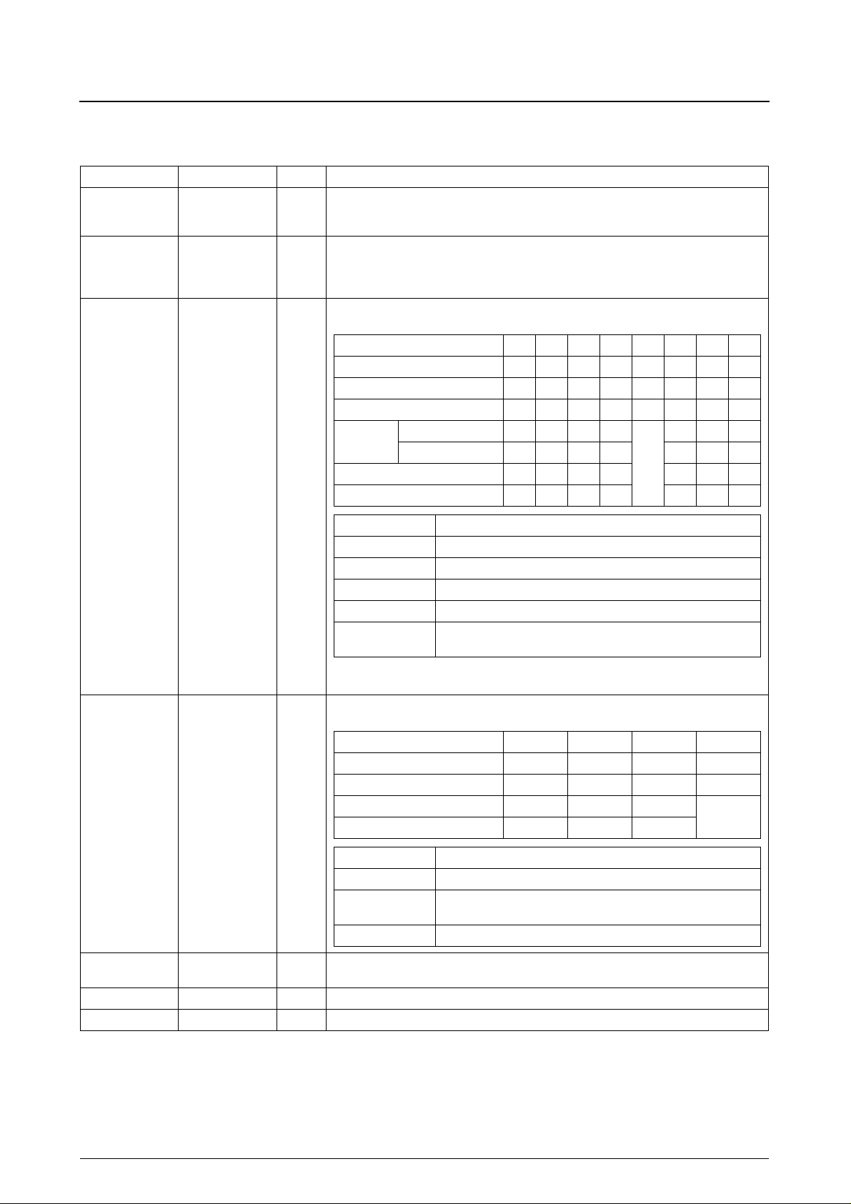
Symbol Pin No. I/O Function
V
DD
V
SS
GSPMD [0:2] 74 to 76 I
9, 18, 29, 37, 43, 49,
54, 60, 68, 73, 90,
109, 126, 144
1, 12, 19, 24, 30, 36,
42, 48, 55, 61, 65,
67, 72, 82, 91, 100,
108, 118, 127, 135
– Supply voltage (+3.3V)
– Ground (0V)
Mode selection signals [0 to 2] for the gray-scale mode. The setting process for the mode selection lines
is described below. GSPMD0 is the LSB and GSPMD2 is the MSB.
Gray-scale mode 01234567
GSPMD0 LHLHLHLH
GSPMD1 L L H H L L H H
GSPMD2 LLLLHHHH
Processing
Number of valid input bits 8888 888
Number of output bits 3456 456
Intra-frame processing Yes Yes Yes Yes
Inter-frame processing Yes Yes Yes Yes No No No
Yes Yes Yes
Reserved
IOMD [0:1] 2, 3 I
Gray-scale mode LCD module
0 Operating mode for TFT LCD modules with 3-bit source driver
1 Operating mode for TFT LCD modules with 4-bit source driver
2, 6 Operating mode for TFT LCD modules with 5-bit source driver
3, 7 Operating mode for TFT LCD modules with 6-bit source driver
5
Do not use gray-scale modes 0 to 3 with TFT LCD modules that perform FRC or other inter-frame
processing.
Input/output mode select pins. The input/output mode selection lines are described below. IOMD0 is the
LSB and IOMD1 is the MSB.
Input/output mode 0123
Input/output mode LCD module
0 XGA-compatible 2-pixel parallel input interface TFT LCD panels
1
2 Serial input interface VGA and SVGA TFT LCD panels
Operating mode for TFT LCD modules with 3-bit source driver that perform
FRC or other inter-frame processing
IOMD0 LHLH
IOMD1 L L H H
Input Parallel Serial Serial
Output Parallel Parallel Serial
2-pixel parallel input interface TFT LCD panels (serial input is converted to
parallel internally)
Reserved
VMD 77 I
SCLK 81 I Clock signal input. Data is processed according to this clock signal.
DSIFT 143 I In input/output mode 1, data is shifted out on both
Gray-scale processing algorithm select pin. The LC11011-141 algorithm is selected when high. Normal
mode is selected when low or open.
D0 and × D1 when high.
No. 5578—4/13
Page 5

×
LC11014-241
Symbol Pin No. I/O Function
SRD0 [7:0] 86 to 89, 92 to 95 I
SRD1 [7:0] 96 to 99, 101 to 104 I
SGD0 [7:0]
SGD1 [7:0]
105 to 107,
110 to 114
115 to 117,
119 to 123
SBD0 [7:0] 124, 125, 128 to 133 I
SBD1 [7:0] 134, 136 to 142 I
SHSYNC 79 I
SVSYNC 80 I
SHDEN 78 I
SCTL 83 I
CLKSEL 8 I
CLK 66 O
CLKB 69 O
RD0 [0:5] 52 to 53, 56 to 59 O
RD1 [0:5] 44 to 47, 50, 51 O
GD0 [0:5] 34, 35, 38 to 41 O
GD1 [0:5] 26 to 28, 31 to 33 O
BD0 [0:5] 17, 20 to 23, 25 O
BD1 [0:5] 10, 11, 13 to 16 O
HSYNC 62 O
VSYNC 63 O
HDEN 64 O
CTL 70 O
PWRSV 84 I
BYPASS 85 I
TEST [0:3] 4 to 7 I Test pins [0:3]; left open for normal operation
NC 71 – Must be left open.
Input pins for red, green and blue gra y-scale data. SRD07, SRD17, SGD07, SGD17, SBD07, SBD17 are
the MSBs. SRD00, SRD10, SGD00, SGD10, SBD00, SBD10 are the LSBs. Input data 00
I
to minimum brightness, and FF
occur when an input is set to either the minimum or maximum. If 2-pixel data is set on both S × D0 and
I
S × D1, the display data on S × D0 is displayed first. In input/output modes 1 and 2, inputs SRD1[0:7],
to maximum brightness. Note that correct gray-scale display does not
H
SGD1[0:7] and SBD1[0:7] should be tied high or low.
Horizontal and vertical synchronization signal inputs. These are the sources for the HSYNC and VSYNC
signals. They are also used to control data processing. Active-low signals.
Horizontal data valid-period signal input. Set this pin high during periods when the horizontal data is
valid. If this signal is not used, tie it high and set the input data to 0 during the horizontal blanking period.
LCD control signal input. Input control signal that must be matched to the data signal timing. This is the
source for the CTL signal. If the CTL signal is not used, there is no internal signal processing of this input
and hence there is no need to input the SCTL signal.
CLKSEL is the dot clock output select pin. It is used to select the output mode of the dot clock signal
output pin.
In input/output modes 0 and 2: When CLKSEL is low, a signal with the opposite phase from SCLK is
output from CLK. When CLKSEL is high, a signal with the same phase as SCLK is output from CLKB.
In input/output mode 1: When CLKSEL is low, a signal with half the frequency of SCLK is output from
CLK. When CLKSEL is high, a signal with the opposite phase from CLK is output from CLKB.
Red, green and blue gray-scale data output pins. RD05, RD15, GD05, GD15, BD05, BD15 are the
MSBs. RD00, RD10, GD00, GD10, BD00, BD10 are the LSBs. If a 2-pixel data set is on
the data on × D0 is displayed first. In input/output modes 1 and 2, outputs RD1[0:5], GD1[0:5] and
BD1[0:5] are low.
In 3-bit data output mode: RD03, RD13, GD03, GD13, BD03, BD13 are the LSBs. RD0[2:0], RD1[2:0],
GD0[2:0], GD1[2:0], BD0[2:0], BD1[2:0] are low.
In 4-bit data output mode: RD02, RD12, GD02, GD12, BD02, BD12 are the LSBs. RD0[1:0], RD1[1:0],
GD0[1:0], GD1[1:0], BD0[1:0], BD1[1:0] are low.
In 3-bit data output mode: RD01, RD11, GD01, GD11, BD01, BD11 are the LSBs. RD0[0], RD1[0],
GD0[0], GD1[0], BD0[0], BD1[0] are low.
Vertical and horizontal synchronization signal outputs. To match the data signal timing, these outputs are
delayed with respect to their input signals. In input/output mode 0, they are delayed by 8 SCLK cycles,
and in input/output modes 1 and 2, they are delayed by 16 SCLK cycles. When PWRSV is high, these
signals are output without being latched internally.
Horizontal data valid-period signal output.To match the data signal timing, this output is delayed with
respect to the input signal. In input/output mode 0, they are delayed by 8 SCLK cycles, and in
input/output modes 1 and 2, they are delayed by 16 SCLK cycles. When PWRSV is high, this signal is
output without being latched internally.
LCD control signal output. To match the data signal timing, this output is delayed with respect to the
SCTL input signal. In input/output mode 0, they are dela y ed by 8 SCLK cycles , and in input/output modes
1 and 2, they are delayed by 16 SCLK cycles. When PWRSV is high, this signal is output without being
latched internally.
Power-save control input. When this input goes high, the internal clock stops and the LSI enters powersave mode. Output data are held high. VSYNC, HSYNC, HDEN and CTL control signals, and either CLK
or CLKB are output without being latched internally. Tie low or leave open for normal operation.
Gray-scale processing bypass pin. When high, the input signals are latched and output without change.
When a high-level input on this pin is sampled on the falling edge of SCLK: in input/output mode 0, output
is delayed by 8 SCLK cycles, and in input/output modes 1 and 2, output is delayed by 16 SCLK cycles.
corresponds
H
D0 and × D1,
No. 5578—5/13
Page 6

Specifications
LC11014-241
−
−
−
°
−
° C
–
−
–
–
–
–
µ
Absolute Maximum Ratings
at V
SS
= 0V
Parameter Symbol Conditions Ratings Unit
Maximum supply voltage V
Input voltage V
Output voltage V
DD
max
IN
O
0.3 to +4.6 V
0.3 to +5.8 V
0.3 to V
+ 0.3 V
DD
Operating temperature Topr 0 to +70
Storage temperature Tstg
Allowable Operating Ranges
at Ta = 0 to +70 ° C
40 to +125
Parameter Symbol Conditions min typ max Unit
Supply voltage V
Input voltage V
Clock frequency
Clock frequency
1
1
Clock frequency f
f
CLK
f
CLK
CLK
DD
IN
Input/output mode 0 – – 40 MHz
Input/output mode 1 – – 65 MHz
Input/output mode 2 – – 50 MHz
3.15 3.3 3.45 V
0 – 5.5 V
1. 1024 ¥ 768; At timing ≥ 60Hz (XGA timing), the display interval is less than 75%.
DC Characteristics
at Ta = 0 to +70 ° C, V
= 0V, V
SS
= 3.15 to 3.45V
DD
Parameter Symbol Conditions min typ max Unit
High-level input voltage V
Low-level input voltage V
High-level output voltage V
Low-level output voltage V
Operating current drain
Power-save current drain
Standby current drain
1. Input/output mode 0, gray-scale mode 7, f
2. Input/output mode 0, PWRSV = low, f
3. V
= 3.3V, all outputs open, all input pins tied low
DD
1
2
3
= 32.5MHz, V
CLK
= 32.5MHz, V
CLK
I
I
CPS
I
CST
IH
IL
OH
OL
CC
DD
= 3.3V, C
DD
I
= − 2mA V
OH
I
= 2mA
OL
= 3.3V, C
= 15pF, (1024 × 768, measured with 60Hz XGA timing)
L
=15pF (control signals: VSYNC, HSYNC, HDEN, CTL, CLK), all other outputs open
L
2.0 – – V
– 0.5 V
0.6 – – V
DD
– 0.4 V
110 170 mA
–30mA
– 100
C
A
No. 5578—6/13
Page 7

LC11014-241
Switching Characteristics
at Ta = 0 to +70 ° C, V
= 0V, V
SS
= 3.15 to 3.45V, C
DD
= 15pF
L
Parameter Symbol min typ max Unit
SCLK cycle time
SCLK cycle time
SCLK cycle time
SCLK high-level pulse width
SCLK high-level pulse width
SCLK high-level pulse width
SCLK low-level pulse width
SCLK low-level pulse width
SCLK low-level pulse width
1
2
3
4
1
2 3
4
1
2 3
4
Tsclk 25 – – ns
Tsclk 15.4 – – ns
Tsclk 20 – – ns
Tschw 10 – – ns
Tschw 6.2 – – ns
Tschw 8 – – ns
Tsclw 10 – – ns
Tsclw 6.2 – – ns
Tsclw 8 – – ns
HSYNC low-level pulse width Thpw 2Tsclk – – ns
HSYNC high-level pulse width Tvpw 2Tsclk – – ns
CLK propagation delay time
CLK propagation delay time
CLKB propagation delay time
CLKB propagation delay time
CLK propagation delay time
CLK propagation delay time
CLKB propagation delay time
CLKB propagation delay time
CLK propagation delay time
CLK propagation delay time
CLKB propagation delay time
CLKB propagation delay time
1
1
1
1
2 3
2 3
2 3
2 3
4
4
4
4
Tpckh 7 11 22 ns
Tpckl 7 11 22 ns
Tpcbh 6 10 20 ns
Tpcbl 7 12 24 ns
Tpckh 7 12 24 ns
Tpckl 8 13 25 ns
Tpcbh 7 12 23 ns
Tpcbl 8 13 26 ns
Tpckh 7 11 22 ns
Tpckl 7 11 22 ns
Tpcbh 6 10 20 ns
Tpcbl 8 12 25 ns
Data setup time Tdsu 5 – – ns
Data hold time Tdhd 5 – – ns
Data output propagation delay time
Data output propagation delay time
Data output propagation delay time
Data output propagation delay time
Data output propagation delay time
Data output propagation delay time
1
2 3
2 3
2 3
2 3
4
Tpdata 8Tsclk + 9 8Tsclk + 14 8Tsclk + 28 ns
Tpdt0sl 16Tsclk + 9 16Tsclk + 15 16Tsclk + 29 ns
Tpdt1sl 15Tsclk + 9 15Tsclk + 15 15Tsclk + 30 ns
Tpdt0sh 15Tsclk + 9 15Tsclk + 15 15Tsclk + 29 ns
Tpdt1sh 16Tsclk + 9 16Tsclk + 15 16Tsclk + 30 ns
Ttdatass 16Tsclk + 9 16Tsclk + 14 16Tsclk + 27 ns
Control signal setup time Tcsu 5 – – ns
Control signal hold time Tchd 5 – – ns
Control signal propagation delay time
Control signal propagation delay time
1
2 3 4
Tpctl 8Tsclk + 8 8Tsclk + 13 8Tsclk + 24 ns
Tpctlsp 16Tsclk + 8 16Tsclk + 13 16Tsclk + 26 ns
1. Parallel input, parallel output
2. Serial input, parallel output (1H number of pixels is even)
3. Serial input, parallel output (1H number of pixels is odd)
4. Serial input, serial output
No. 5578—7/13
Page 8

LC11014-241
Timing Diagrams
Input/output mode 0 (parallel input, serial output)
No. 5578—8/13
Page 9

LC11014-241
Input/output mode 1 (serial input, parallel output: 1H number of pixels is even)
No. 5578—9/13
Page 10

LC11014-241
Input/output mode 1 (serial input, parallel output: 1H number of pixels is odd)
No. 5578—10/13
Page 11

LC11014-241
Input/output mode 2 (serial input, serial output)
No. 5578—11/13
Page 12

Usage Notes
Parallel input, parallel output
LC11014-241
Serial input, parallel output
No. 5578—12/13
Page 13

Serial input, serial output
Usage Note
LC11014-241
Since this LSI performs spatial modulation using an error
diffusion algorithm, patterns that differ from the original
images may be displayed for certain display pattern and
gray-scale mode combinations.
■
No products described or contained herein are intended for use in surgical implants, life-support systems, aerospace equipment, nuclear
power control systems, vehicles, disaster/crime-pre v ention equipment and the lik e, the failure of which may directly or indirectly cause injury,
death or property loss.
■
Anyone purchasing any products described or contained herein for an above-mentioned use shall:
➀
Accept full responsibility and indemnify and defend SANYO ELECTRIC CO., LTD., its affiliates, subsidiaries and distributors and all their
officers and employees, jointly and severally, against any and all claims and litigation and all damages, cost and expenses associated
with such use:
➁
Not impose any responsibility for any fault or negligence which may be cited in any such claim or litigation on SANYO ELECTRIC CO.,
LTD., its affiliates, subsidiaries and distributors or any of their officers and employees, jointly or severally.
■
Information (including circuit diagrams and circuit parameters) herein is for e xample only; it is not guaranteed for volume production. SANYO
believes information herein is accurate and reliable, but no guarantees are made or implied regarding its use or any infringements of
intellectual property rights or other rights of third parties.
This catalog provides information as of June, 1997. Specifications and information herein are subject to change without notice.
No. 5578—13/13
 Loading...