

Page 1
Overview
The LC11011-141 is a pseudo gray scale processor for
TFT LCD. It allows LCD panels with inputs of three to six
bits per RGB to display the equivalent of 16.7 million
colors.
Features
• Handles 8-bits of input data (256-scale data) for each of
the RGB colors.
• Operating mode selection of three, four, or six bit driver
outputs
• Realizes reduced resolution loss (as compared to
dithering techniques) by using intra- and inter-frame
error diffusion processing.
• Supports both 5 V and low voltage (3.3 V) operation.
• Operates with arbitrary clock frequencies up to 50 MHz
(at 5 V) or up to 30 MHz (at 3.3 V).
• Can operate independently of the number of displayed
pixels since internal operation is controlled by the
horizontal and vertical synchronization signals.
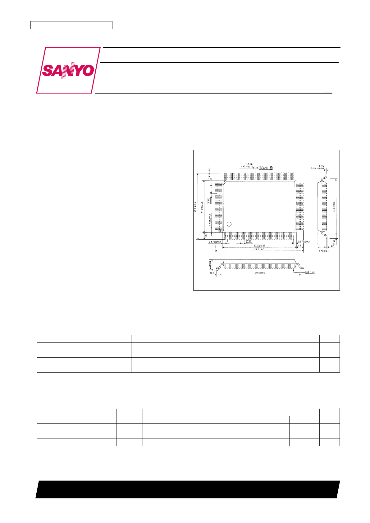
Package Dimensions
unit: mm
3151-QFP100E
CMOS LSI
22896HA (OT)/No. 5041-1/7
Preliminaly
SANYO: QFP100E
[LC11011-141]
SANYO Electric Co.,Ltd. Semiconductor Bussiness Headquarters
TOKYO OFFICE Tokyo Bldg., 1-10, 1 Chome, Ueno, Taito-ku, TOKYO, 110 JAPAN
Computer Image Signal Processing
Full-Color Gray-Scale Processor
LC11011-141
Ordering number : EN*5041A
Specifications
Absolute Maximum Ratings at Ta = 25°C, VSS= 0 V
Electrical Characteristics: At an operating voltage of 5.0 V
Operating Ranges at Ta = 0 to +70°C
Parameter Symbol Conditions Ratings Unit
Maximum supply voltage V
DD
max –0.3 to +7.0 V
Input and output voltages V
I
, V
O
–0.3 to VDD+ 0.3 V
Operating temperature Topr 0 to +70 °C
Storage temperature Tstg –40 to +125 °C
Parameter Symbol Conditions
Ratings
Unit
min typ max
Supply voltage V
DD
4.5 5.0 5.5 V
Input voltage V
IN
0V
DD
V
Clock frequency f
clk
50 MHz
Page 2

No. 5041-2/7
LC11011-141
DC Characteristics at Ta = 0 to +70°C, VSS= 0 V, VDD= 4.5 to 5.5 V
Note: * The test conditions are: fCP= 25.175 MHz, VDD= 5.0 V, CL= 15 pF (measured with VGA timing)
Switching Characteristics at Ta = 0 to +70°C, VSS= 0 V, VDD= 4.5 to 5.5 V, CL= 15 pF
Electrical Characteristics: At an operating voltage of 3.3 V
Operating Ranges at Ta = 0 to +70°C
DC Characteristics at Ta = 0 to +70°C, V
SS
= 0 V, VDD= 3.0 to 3.6 V
Note: * The test conditions are: f
clk
= 25.175 MHz, VDD= 3.3 V, CL= 15 pF (measured with VGA timing)
Parameter Symbol Conditions
Ratings
Unit
min typ max
High level input voltage V
IH
CMOS level 0.7 V
DD
V
Low level input voltage V
IL
CMOS level 0.3 V
DD
V
High level output voltage V
OH
IOH(–4 mA) 2.4 V
Low level output voltage V
OL
IOL(4 mA) 0.4 V
Supply current I
CC
* 40 70 mA
Parameter Symbol Conditions
Ratings
Unit
min typ max
High level input voltage V
IH
CMOS level 0.7 V
DD
V
Low level input voltage V
IL
CMOS level 0.3 V
DD
V
High level output voltage V
OH
IOH(–2 mA) 2.2 V
Low level output voltage V
OL
IOL(2 mA) 0.4 V
Supply current I
CC
* 30 45 mA
Parameter Symbol Conditions
Ratings
Unit
min typ max
Dot clock cycle time Tdclk 20 ns
Hsync low level pulse width Thpw 2 Tdclk ns
Vsync low level pulse width Tvpw 2 Tdclk ns
Data setup time Tdsu 5 ns
Data hold time Tdhd 5 ns
Control signal setup time Tcsu 5 ns
Control signal hold time Tchd 5 ns
CLK propagation delay time Ttdhh 2 3 6 ns
CLK propagation delay time Ttdll 2 4 7 ns
CLKB propagation delay time Ttdhl 2 4 7 ns
CLKB propagation delay time Ttdlh 2 4 7 ns
Control signal propagation delay time Ttctl 2 Tdclk + 3 2 Tdclk + 6 2 Tdclk + 10 ns
Data output propagation delay time Ttdata 2 Tdclk + 3 2 Tdclk + 6 2 Tdclk + 11 ns
Parameter Symbol Conditions
Ratings
Unit
min typ max
Supply voltage V
DD
3.0 3.3 3.6 V
Input voltage V
IN
0 V
DD
V
Clock frequency f
clk
30 MHz
Page 3

No. 5041-3/7
LC11011-141
Switching Characteristics at Ta = 0 to +70°C, VSS= 0 V, VDD= 3.0 to 3.6 V, CL= 15 pF
Pin Assignment
Parameter Symbol Conditions
Ratings
Unit
min typ max
Dot clock cycle time Tdclk 33 ns
Hsync low level pulse width Thpw 2 Tdclk ns
Vsync low level pulse width Tvpw 2 Tdclk ns
Data setup time Tdsu 10 ns
Data hold time Tdhd 10 ns
Control signal setup time Tcsu 10 ns
Control signal hold time Tchd 10 ns
CLK propagation delay time Ttdhh 2 5 12 ns
CLK propagation delay time Ttdll 2 6 14 ns
CLKB propagation delay time Ttdhl 2 6 14 ns
CLKB propagation delay time Ttdlh 2 6 14 ns
Control signal propagation delay time Ttctl 2 Tdclk + 5 2 Tdclk + 10 2 Tdclk + 22 ns
Data output propagation delay time Ttdata 2 Tdclk + 5 2 Tdclk + 10 2 Tdclk + 24 ns
Page 4

No. 5041-4/7
LC11011-141
Block Diagram
Page 5

No. 5041-5/7
LC11011-141
Pin Functions
Symbol Pin No. I/O Function
V
DD
5, 21, 28, 32, 41,
Input Power supply (+5 V)
61, 68, 91
10, 15, 20, 26, 30,
V
SS
34, 35, 40, 46,51,
Input
GND (0 V)
56, 66, 71, 73, 82,
87, 90, 98
NC 24, 76, 77 — Must be left open.
MODESEL0 1 Input
MODESEL1 2 Input
MODESEL2 3 Input
MODESEL3 4 Input
Input bypass pin. When this pin is low, the LC11011-141 performs no gray scale processing, but rather
BYPASS 100 Input simply passes the input signals through unchanged. When a low level input on this pin is sampled on the
rising edge of the clock, the IC will begin the output of unchanged data two clock cycles later.
TEST0 6 Input
TEST1 7 Input
Test pins [0:3]; left open in normal operation.
TEST2 8 Input
TEST3 9 Input
SCLK 67 Input Display dot clock input. Data is processed according to this clock signal.
SRDATA [0:7] 57 to 60, 62 to 65 Input
Input pins for red, green and blue scale data. SRDATA7, SGDATA7, and SBDATA7 are the MSBs.
SGDATA [0:7] 78 to 81, 83 to 86 Input
SRDATA0, SGDATA0, and SBDATA0 are the LSBs.
SBDATA [0:7] 88, 89, 92 to 97 Input
Shsync 69 Input
Horizontal and vertical synchronization signal inputs. These are the sources for the Hsync and Vsync
Svsync 70 Input
signals. These are also used to control data processing. These are low level active signals.
Horizontal data valid period signal input. Set this pin high during periods when the horizontal data is
SHDEN 72 Input valid. If this signal is not used, tie it high, and set the input data to zero during the horizontal blanking
period.
SCTL0 74 Input
LCD control inputs. Input control signals that must be matched to the data signal timing. These are the
sources for the CTL signals. If the CTL [0:1] signals are not used, there is no need to input the
SCTL1 75 Input
SCTL [0:1] signals.
CLKSEL 99 Input
CLKSEL is the dot clock output selection. It is used to select the output mode of the dot clock signal
CLK 31 Output
output pin.
If CLKSEL is low: A signal with the same phase as the SCLK pin is output from the CLK pin.
CLKB 33 Output If CLKSEL is high: A signal with the opposite phase from the SCLK pin is output from the CLKB pin.
Mode selection signals [0:3] for the gray scale mode.
The setting process for the mode selection lines is described below.
MODESEL0 is the LSB, and MODESEL3 is the MSB.
Note that modes 8, 9, C, D and E are compatible with the LC1001-131 (a product that handles 6-bits
of input for each of the RGB signals).
Note: Do not use gray scale modes 0, 1, 3, 8 and 9 with LCD modules that perform FRC or other inter-
frame processing.
Note: Y = yes, N = no, R = reserved
Color scale mode 0 1 2 3 4 5 6 7 8 9 A B C D E F
MODESEL0 L H L H L H L H L H L H L H L H
MODESEL1 L L H H L L H H L L H H L L H H
MODESEL2 L L L L H H H H L L L L H H H H
MODESEL3 L L L L L L L L H H H H H H H H
Intra-frame
Y Y Y Y Y Y Y Y Y Y Y
R
processing
R R R RProcessing
Inter-frame
Y Y Y N N N Y Y N N N
processing
Number of valid input bits 8 8 8 8 8 8 6 6 6 6 6
Number of output bits 3 4 6 4 5 6 3 4 3 4 5
Gray scale modes 0, 8 and C Operating mode for TFT-LCD modules using 3-bit source drivers.
Gray scale modes 1 and 9 Operating mode for TFT-LCD modules using 4-bit source drivers.
Gray scale mode 3 Operating mode for TFT-LCD modules using 6-bit source drivers.
Gray scale modes 5 and D
Operating mode for TFT-LCD modules that perform
FRC or other inter-frame processing.
Gray scale modes 6, 7 and E
Operating mode for TFT-LCD modules that perform FRC or other
inter-frame processing.
Continued on next page.
Page 6

No. 5041-6/7
LC11011-141
Continued from preceding page.
Timing Chart
Symbol Pin No. I/O Function
Red, green and blue gray scale data output pins. These are delayed by 2 clock cycles with respect to the
RDATA [0:7] 11 to 14, 16 to 19 Output
input data.
RDATA7, GDATA7 and BDATA7 are the MSBs.
In modes 0, 8, C and F, RDATA5, GDATA5 and BDATA5 are the LSBs. In these modes, RDATA [0:4],
GDATA [0:4] and BDATA [0:4] are not used.
GDATA [0:7] 36 to 39, 42 to 45 Output
In modes 1, 5, 9 and D, RDATA4, GDATA4 and BDATA4 are the LSBs. In these modes, RDATA [0:3],
GDATA [0:3] and BDATA [0:3] are not used.
In modes 6 and E, RDATA3, GDATA3 and BDATA3 are the LSBs. In these modes, RDATA [0:2],
GDATA [0:2] and BDATA [0:2] are not used.
BDATA [0:7] 47 to 50, 52 to 55 Output
In modes 3 and 7, RDATA2, GDATA2 and BDATA2 are the LSBs. In these modes, RDATA [0:1],
GDATA [0:1] and BDATA [0:1] are not used.
Vsync 27 Output
Horizontal and vertical synchronization signal outputs. To match the data signal timing these are delayed
Hsync 29 Output
by two clock cycles with respect to their input signals.
HDEN 25 Output Horizontal data valid period signal output
CLT0 22 Output
LCD control signal outputs. To match the data signal timing these are delayed by two clock cycles with
CLT1 23 Output
respect to the SCTL [0:1] input signals.
Page 7

No. 5041-7/7
LC11011-141
This catalog provides information as of December, 1997. Specifications and information herein are subject to
change without notice.
■ No products described or contained herein are intended for use in surgical implants, life-support systems, aerospace
equipment, nuclear power control systems, vehicles, disaster/crime-prevention equipment and the like, the failure of
which may directly or indirectly cause injury, death or property loss.
■ Anyone purchasing any products described or contained herein for an above-mentioned use shall:
➀ Accept full responsibility and indemnify and defend SANYO ELECTRIC CO., LTD., its affiliates, subsidiaries and
distributors and all their officers and employees, jointly and severally, against any and all claims and litigation and all
damages, cost and expenses associated with such use:
➁ Not impose any responsibility for any fault or negligence which may be cited in any such claim or litigation on
SANYO ELECTRIC CO., LTD., its affiliates, subsidiaries and distributors or any of their officers and employees
jointly or severally.
■ Information (including circuit diagrams and circuit parameters) herein is for example only; it is not guaranteed for
volume production. SANYO believes information herein is accurate and reliable, but no guarantees are made or implied
regarding its use or any infringements of intellectual property rights or other rights of third parties.
Usage Note
Since this LSI performs spatial modulation using an error diffusion algorithm, patterns that differ from the original
images may be displayed for certain display pattern and gray-scale mode combinations.
Continued from preceding page.
 Loading...