

Page 1
Ordering number : EN5974
O3098RM (OT) No. 5974-1/8
Overview
The LB1980H is a 3-phase brushless motor driver that is
particularly appropriate for VCR capstan motor drivers.
Functions
· 3-phase full-wave drive
· Built-in torque ripple correction circuit (variable
correction ratio)
· Current limiter circuit
· Upper and lower side output stage over-saturation
prevention circuit that does not require external
capacitors.
· FG amplifier
· Thermal shutdown circuit
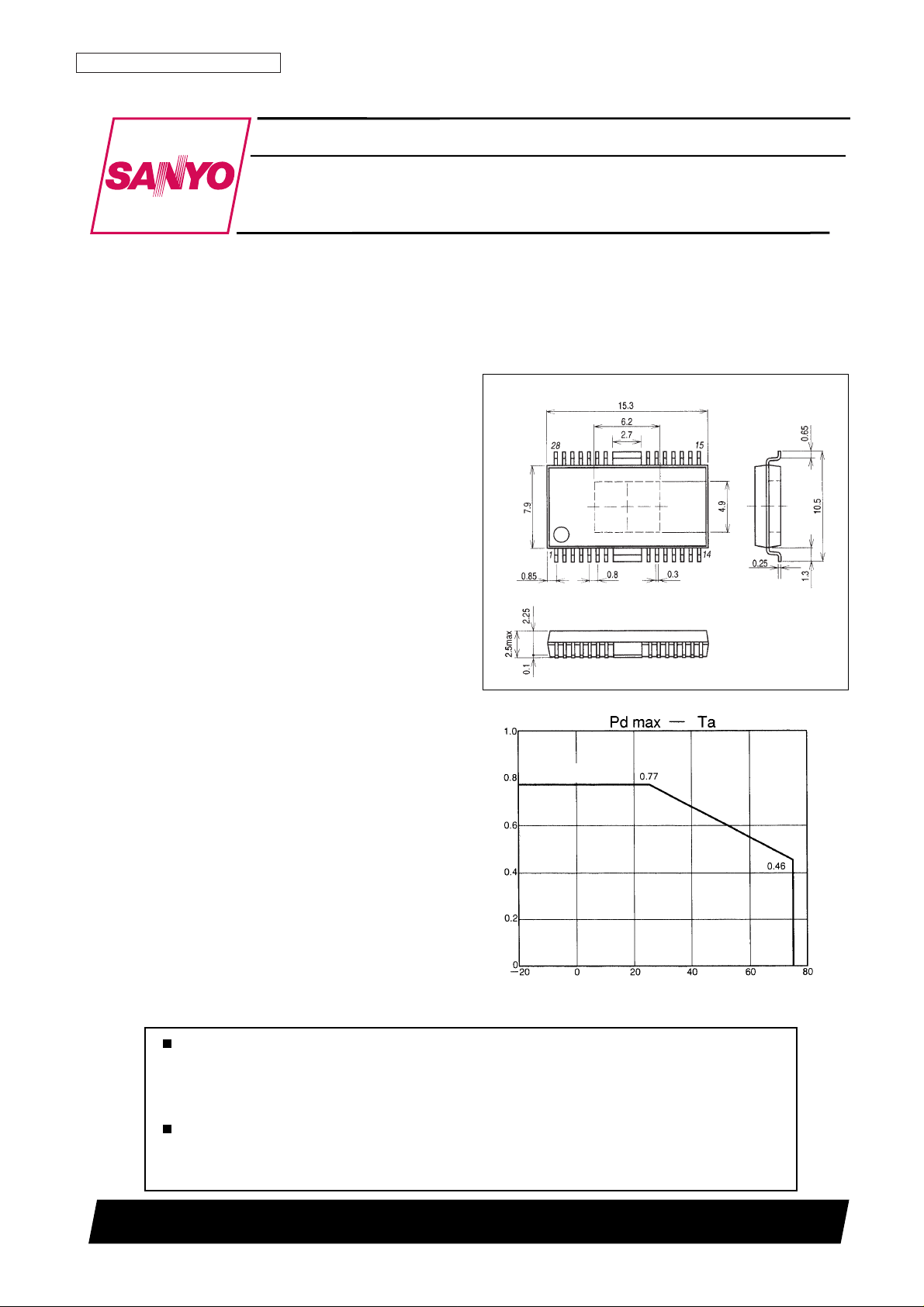
Package Dimensions
unit: mm
3233-HSOP28H
SANYO: HSOP28H
[LB1980H]
LB1980H
SANYO Electric Co.,Ltd. Semiconductor Bussiness Headquarters
TOKYO OFFICE Tokyo Bldg., 1-10, 1 Chome, Ueno, Taito-ku, TOKYO, 110-8534 JAPAN
Three-Phase Brushless Motor Driver
for VCR Capstan Motors
Monolithic Digital IC
Any and all SANYO products described or contained herein do not have specifications that can handle
applications that require extremely high levels of reliability, such as life-support systems, aircraft’s
control systems, or other applications whose failure can be reasonably expected to result in serious
physical and/or material damage. Consult with your SANYO representative nearest you before using
any SANYO products described or contained herein in such applications.
SANYO assumes no responsibility for equipment failures that result from using products at values that
exceed, even momentarily, rated values (such as maximum ratings, operating condition ranges, or other
parameters) listed in products specifications of any and all SANYO products described or contained
herein.
Allowable power dissipation, Pdmax — W
Ambient temperature, Ta — °C
Independent IC
Page 2
Specifications
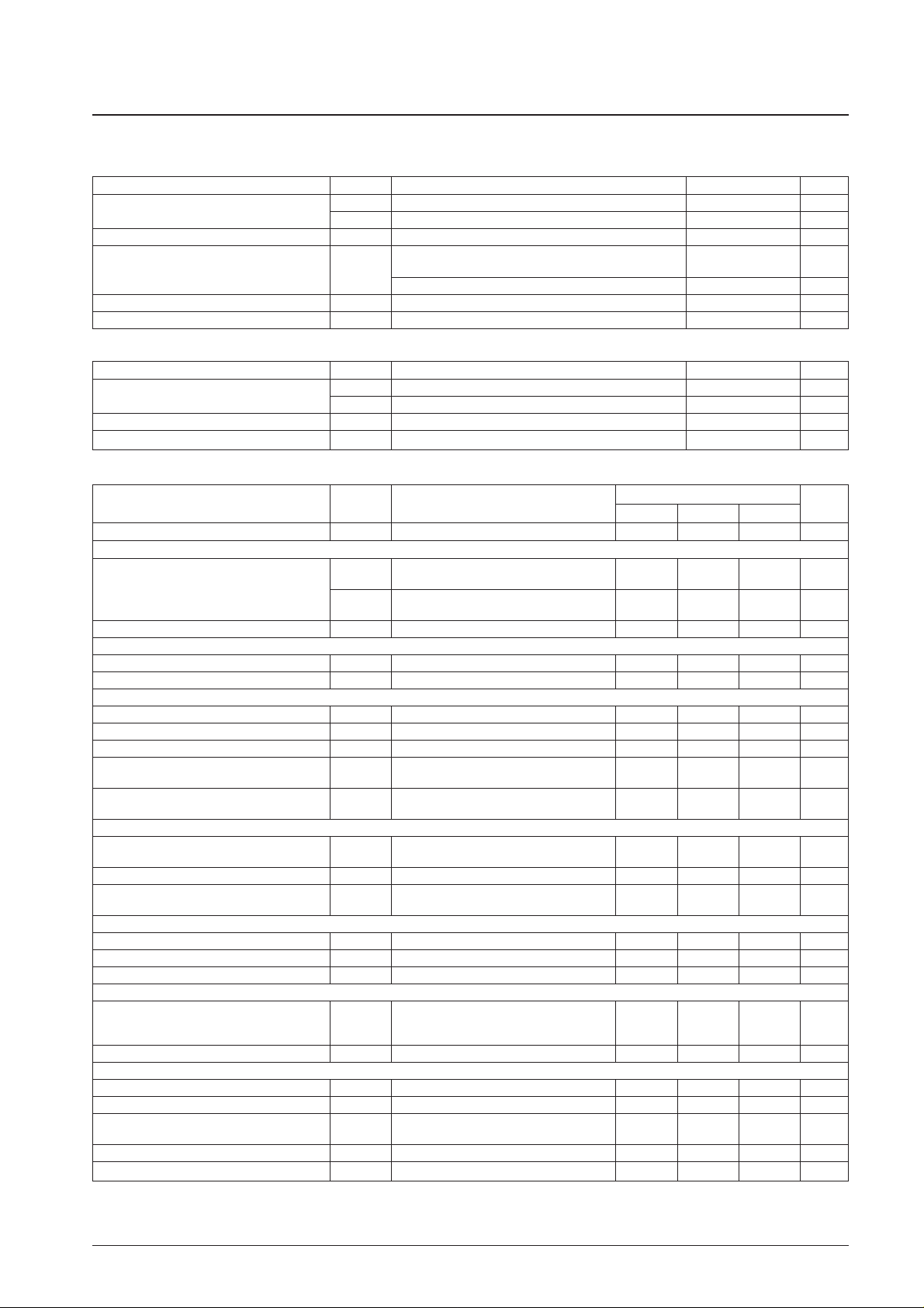
Absolute Maximum Ratings at Ta = 25°C
Allowable Operating Ranges at Ta = 25°C
Electrical Characteristics at Ta = 25°C, VCC= 5 V, VS= 15 V
Notes : 1.The torque ripple correction ratio is determined as follows from the Rf voltage waveform. Continued on next page.
2.Parameters that are indicated as design target values in the conditions column are not tested.
No. 5974-2/8
LB1980H
Parameter Symbol Conditions Ratings Unit
Maximum supply voltage
V
CC
max 7 V
V
S
max 24 V
Maximum output current I
O
max 1.3 A
Mounted on a 71.6
× 114.3 × 1.6 mm glass Epoxy printed
1.81 W
Allowable power dissipation Pd max
circuit board
Independent device 0.77 W
Operating temperature Topr –20 to + 75 °C
Storage temperature Tstg –55 to + 150 °C
Parameter Symbol Conditions Ratings Unit
Supply voltage
V
S
5 to 22 V
V
CC
4.5 to 5.5 V
Hall input amplitude V
HALL
Between the Hall inputs ±30 to ±80 mVo-p
GSENSE pin input range V
GSENSE
With respect to the control system ground –0.20 to + 0.20 V
Parameter Symbol Conditions
Ratings
Unit
min typ max
V
CC
supply current I
CC
RL = ∞, V
CTL
= 0 V, V
LIM
= 0 V (Quiescent) 12 18 mA
[Outputs]
V
O
sat1
I
O
= 500 mA, Rf = 0.5 Ω, Sink + Source
2.1 2.6 V
Output saturation voltage
V
CTL
= V
LIM
= 5 V
(With saturation prevention)
VOsat2
I
O
= 1.0 A, Rf = 0.5 Ω, Sink + Source
2.6 3.5 V
V
CTL
= V
LIM
= 5 V
(With saturation prevention)
Output leakage current IOleak 1.0 mA
[FR]
FR pin input threshold voltage V
FSR
2.25 2.50 2.75 V
FR pin input bias current I
B
(FSR) –5.0 µA
[Control]
CTLREF pin voltage V
CREF
2.05 2.15 2.25 V
CTLREF pin input range V
CREFIN
1.50 3.50 V
CTL pin input bias current I
B
(CTL) With V
CTL
= 5 V and the CTLREF pin open 4.0 µA
CTL pin control start voltage
V
CTL
(ST)
With Rf = 0.5 Ω, V
LIM
= 5 V, IO≥ 10 mA,
2.00 2.15 2.30 V
Hall input logic fixed (U, V, W = H, H, L)
CTL pin control Gm
Gm (CTL)
With Rf = 0.5 Ω, ∆I
O
= 200 mA,
0.46 0.58 0.70 A/V
Hall input logic fixed (U, V, W = H, H, L)
[Current Limiter]
LIM current limit offset voltage Voff (LIM)
With Rf = 0.5 Ω, V
CTL
= 5 V, IO≥ 10 mA,
140 200 260 mV
Hall input logic fixed (U, V, W = H, H, L)
LIM pin input bias current I
B
(LIM) With V
CTL
= 5 V and the V
CREF
pin open –2.5 µA
LIM pin current control level I
LIM
With Rf = 0.5 Ω, V
CTL
= 5 V, V
LIM
= 2.06 V,
830 900 970 mA
Hall input logic fixed (U, V, W = H, H, L)
[Hall Amplifier]
Hall amplifier input offset voltage
Voff (HALL) –6 +6 mV
Hall amplifier input bias current IB(HALL) 1.0 3.0 µA
Hall amplifier common-mode input voltage range
VCM(HALL) 1.3 3.3 V
[TRC]
For the high and low peaks in the
Torque ripple correction ratio TRC Rf waveform when I
O
= 200 mA. 9 %
(Rf = 0.5 Ω, with the ADJ pin open)
*1
ADJ pin voltage V
ADJ
2.37 2.50 2.63 V
[FG Amplifier]
FG amplifier input offset voltage Voff (FG) –8 +8 mV
FG amplifier input bias current I
B
(FG) –100 nA
FG amplifier output saturation voltage V
O
sat (FG)
Sink side, for the load provided by the
0.5 V
internal pull-up resistor
FG amplifier voltage gain V
G
(FG) For the open loop state with f = 10 kHz 41.5 44.5 47.5 dB
FG amplifier common-mode input voltage V
GM
(FG) 0.5 4.0 V
Page 3
Continued from preceding page.
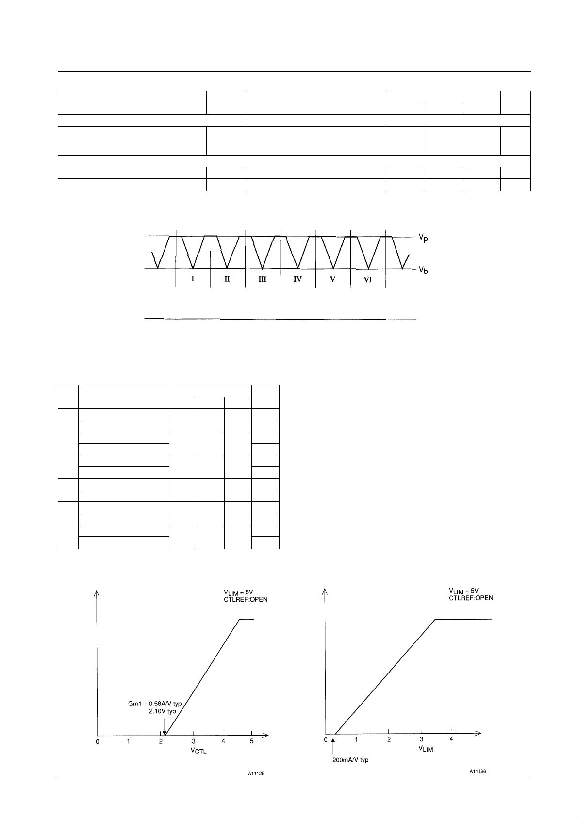
Notes : 1.The torque ripple correction ratio is determined as follows from the Rf voltage waveform.
2.Parameters that are indicated as design target values in the conditions column are not tested.
Truth Table and Control Functions
No. 5974-3/8
LB1980H
Parameter Symbol Conditions
Ratings
Unit
min typ max
[Saturation]
Saturation prevention circuit lower
The voltages between each OUT and
side voltage setting
VOsat (DET)
Rf pair when IO= 10 mA, Rf = 0.5 Ω, and 0.175 0.25 0.325 V
V
CTL
= V
LIM
= 5 V
[TSD]
TSD operating temperature TSD Design target value
*2
180 °C
Hysteresis width ∆TSD Design target value
*2
20 °C
Correction ratio =
2 × (Vp– Vb)
100 × (%)
Vp– V
b
For each Hall logic setting
Ground level
Source → Sink
Hall input
FR
U V W
1
Phase V → Phase W
H H L
H
Phase W → Phase V L
2
Phase U → Phase W
H L L
H
Phase W → Phase U L
3
Phase U → Phase V
H L H
H
Phase V → Phase U L
4
Phase W → Phase V
L L H
H
Phase V → Phase W L
5
Phase W → Phase U
L H H
H
Phase U → Phase W L
6
Phase V → Phase U
L H L
H
Phase U → Phase V L
Note: In the FR column, “H” refers to a voltage of 2.75 V or higher, and “L” refers
to 2.25 V or lower (when V
CC
= 5 V.)
Note: In the Hall input column, “H” refers to the state in the corresponding phase
where the + input is at a potential at least 0.01 V higher than the – input,
and “L” refers to the state where the – input is at a potential at least 0.01 V
higher than the + input.
Note: Since the drive technique adopted is a 180° technique, phases
other than the sink and source phase do not turn off.
Control Function and Current Limiter Function
Control Characteristics Control Limiter Characteristics
Slope: 0.50 A/V (typical)
I
OUT
I
OUT
Page 4
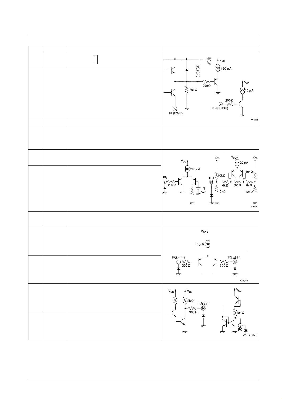
Pin Descriptions
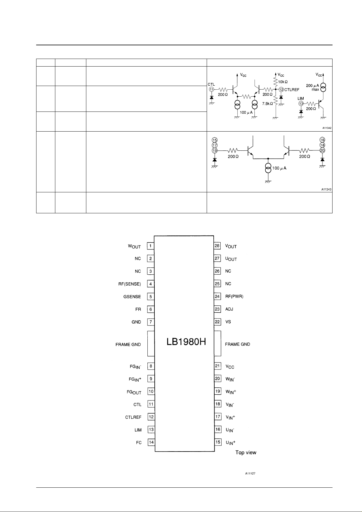
Pin No. Pin Function Equivalent circuit
Used for external adjustment of the torque ripple correction
ratio. Apply a voltage externally with a low-impedance circuit
to the ADJ pin to adjust the correction ratio. The correction
ratio falls as the applied voltage is increased, and increases
as the applied voltage decreases. The torque ripple
correction ratio can be modified by factors in the range 0 to 2
times the ratio that applies when his pin is left open.
(The pin voltage is set to about V
CC
/2 internally, and the
input impedance is about 5 kΩ.)
23 ADJ
Output block power supply
Output current detection. The control block current limiter
operates using the resistor Rf connected between these pins
and ground. Also, the lower side saturation prevention circuit
and the torque ripple correction circuit operate based on the
voltages across this resistor. It is especially important to note
that, since the saturation prevention level is set using this
voltage, the lower side saturation prevention circuit will
become less effective in the high current region if the value of
Rf is lowered excessively. Also, the PWR and SENSE pins
must be connected together.
U phase output
V phase output (Spark killer diodes are built-in.)
W phase output
No. 5974-4/8
LB1980H
27
28
1
U
OUT
V
OUT
W
OUT
4
24
Rf (SENSE)
Rf (PWR)
22
V
S
Ground sensing. The influence of the common ground
impedance on Rf can be excluded by connecting this pin to
nearest ground for the Rf resistor side of the motor ground
wiring that includes Rf. (This pin must not be left open.)
5 GSENSE
Forward/reverse selection. The voltage applied to this pin
selects the motor direction (forward or reverse).
(Vth = 2.5 V at V
CC
= 5 V (typical))
6 FR
Ground for all circuits other than the output transistors. The
lowest potential of the output transistors is that of the Rf pin.
7 GND
Input used when the FG amplifier is used as an inverting
input. A feedback resistor must be connected between
FG
OUT
and this pin.
8
FG
IN
+
Noninverting input used when the FG amplifier is used as a
differential input amplifier. No bias is applied internally.
9
FG
IN
–
FG amplifier output. There is an internal resistive load.10
FG
OUT
Speed control loop frequency characteristics correction.14 FC
Continued on next page.
OUT
Lower side saturation
prevention circuit input block
Page 5
Continued from preceeding page.
Pin Assignment
Pin No. Pin Function Equivalent circuit
Control reference voltage. While this pin is set to about
0.43 × V
CC
internally, this voltage can be modified by
applying a voltage from a low-impedance circuit.
(The input impedance is about 4.3 kΩ).
CTLREF12
CTL
Speed control input. The control implemented is fixed current
drive controlled by current feedback from Rf.
Gm = 0.58/V (typical) when Rf = 0.5 Ω
11
LIM
Current limiter function control. The output current can be
varied linearly by applying a voltage to this pin.
The slope is 0.5 A/V (typical) when Rf = 0.5 Ω.
13
V
CC
Power supply for all internal blocks other than the output
block. This voltage must be stabilized so that noise and ripple
do not enter the IC.
21
U
IN
+
U
IN
–
V
IN
+
V
IN
–
W
IN
+
W
IN
–
U phase Hall element inputs.
Logic high is defined as states where IN+> IN
–
.
V phase Hall element inputs.
Logic high is defined as states where IN+> IN
–
.
W phase Hall element inputs.
Logic high is defined as states where IN+> IN
–
.
15
16
17
18
19
20
No. 5974-5/8
LB1980H
Page 6
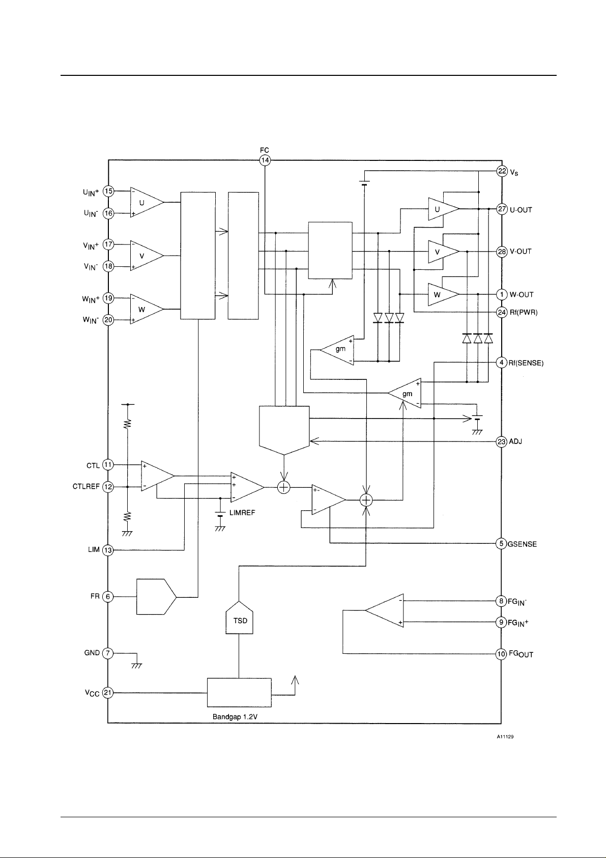
Block Diagram
No. 5974-6/8
LB1980H
Control
amplifier
Reference
voltage
About
0.43 × V
CC
Forward/
reverse
selection
Differential
distribution and
torque ripple
correction
block
Drive distribution circuit
and lower side saturation
prevention circuit
Feedback
amplifier
FG amplifier
Antilogarithm
conversion
and
differential
distribution
Upper side
saturation
prevention
control
Output stage
Hall input synthesis block
(linear matrix)
Synthesized output logarithmic
compression block
Page 7
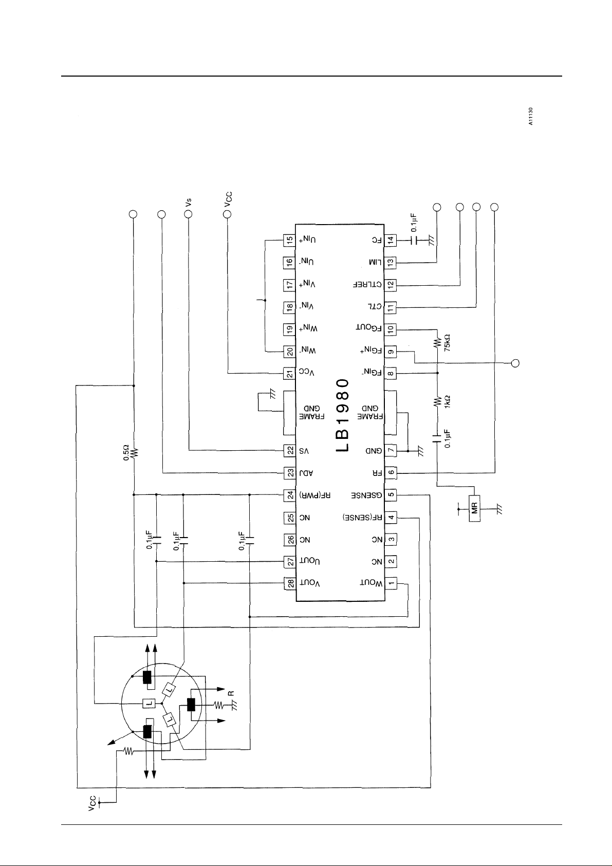
Sample Application Circuit
No. 5974-7/8
LB1980H
GaAs Hall devices
are recommended.
Hall output
Hall output
Hall output
Hall
output
V
CC
/2 bias
Power system ground
Voltage applied to the
ADJ pin
Current limiter setting
voltage pin
CTLREF voltage pin
Torque command
voltage pin
Forward/reverse
command voltage pin
Page 8
PS No. 5974-8/8
LB1980H
This catalog provides information as of October, 1998. Specifications and information herein are subject
to change without notice.
Specifications of any and all SANYO products described or contained herein stipulate the performance,
characteristics, and functions of the described products in the independent state, and are not guarantees
of the performance, characteristics, and functions of the described products as mounted in the customer’s
products or equipment. To verify symptoms and states that cannot be evaluated in an independent device,
the customer should always evaluate and test devices mounted in the customer’s products or equipment.
SANYO Electric Co., Ltd. strives to supply high-quality high-reliability products. However, any and all
semiconductor products fail with some probability. It is possible that these probabilistic failures could
give rise to accidents or events that could endanger human lives, that could give rise to smoke or fire,
or that could cause damage to other property. When designing equipment, adopt safety measures so
that these kinds of accidents or events cannot occur. Such measures include but are not limited to protective
circuits and error prevention circuits for safe design, redundant design, and structural design.
In the event that any or all SANYO products (including technical data, services) described or contained
herein are controlled under any of applicable local export control laws and regulations, such products must
not be exported without obtaining the export license from the authorities concerned in accordance with the
above law.
No part of this publication may be reproduced or transmitted in any form or by any means, electronic or
mechanical, including photocopying and recording, or any information storage or retrieval system,
or otherwise, without the prior written permission of SANYO Electric Co., Ltd.
Any and all information described or contained herein are subject to change without notice due to
product/technology improvement, etc. When designing equipment, refer to the “Delivery Specification”
for the SANYO product that you intend to use.
Information (including circuit diagrams and circuit parameters) herein is for example only; it is not
guaranteed for volume production. SANYO believes information herein is accurate and reliable, but
no guarantees are made or implied regarding its use or any infringements of intellectual property rights
or other rights of third parties.
 Loading...