

Page 1
Ordering number: EN4392A
Monolithic Digital IC
LB1674V
Brushless, Sensorless Motor Driver
Overview
The LB1674V is a small motor driver ideal for mini-cassettes,
headphone stereos and micro-cassettes.
Functions and Features
c 3-phase unipolar, brushless, sensorless motor driver
c Reverse function
c Built-in speed control function (V servo)
c Built-in reference voltage (0.5 V)
c Soft switching driver
Specifications
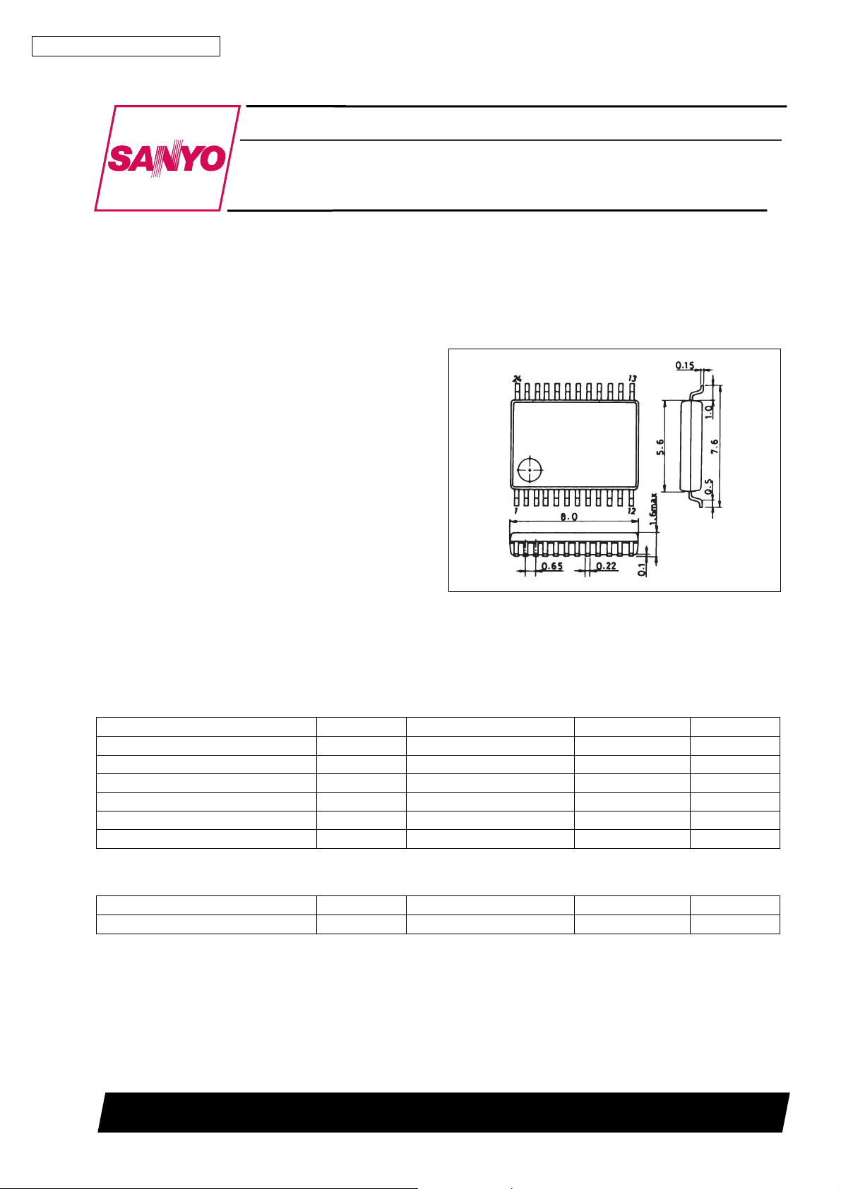
Package Dimensions
unit : mm
3175A-SSOP24
[LB1674V]
SANYO : SSOP24
Absolute Maximum Ratings at Ta = 25°C
Parameter Symbol Conditions Ratings Unit
Maximum supply voltage V
Output transistor withstand voltage Vsus 10 V
Maximum output current Im max 0.6 A
Allowable power dissipation Pd max Tj = 125°C 0.4 W
Operating temperature Topr 0 to + 80 °C
Storage temperature Tstg –40 to + 125 °C
max 5 V
CC
Allowable Operating Range at Ta = 25°C
Parameter Symbol Conditions Ratings Unit
Supply voltage V
CC
1.0 to 3.5 V
SANYO Electric Co.,Ltd. Semiconductor Bussiness Headquarters
TOKYO OFFICE Tokyo Bldg., 1-10, 1 Chome, Ueno, Taito-ku, TOKYO, 110 JAPAN
83096HA(II)/90793TS No.4392-1/6
Page 2
LB1674V
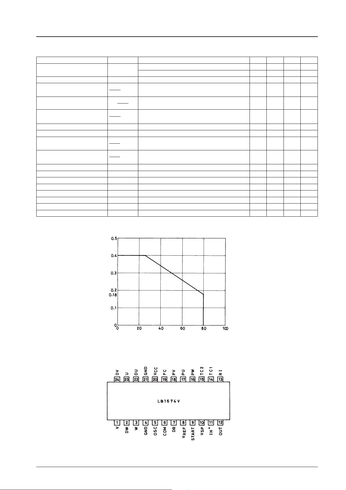
Electrical Characteristics at Ta = 25°C, VCC= 1.5 V, unless otherwise noted
Parameter Symbol Conditions min typ max Unit
Supply current I
Reference voltage Vref 0.47 0.50 0.53 V
Reference-voltage characteristic
Reference-voltage load
characteristics
Reference-voltage temperature
characteristics
Speed signal detection accuracy Vsp V
Speed signal interphase error –5 +5 %
Speed-signal voltage
characteristics
Speed-signal temperature
characteristics
Current detection accuracy V
Current detection ratio K
Starting pulse period T
COM* lead-in current I
Output saturation voltage Vsat V
Logic input high-level voltage V
Logic input low-level voltage V
TC pin lead-in current I
∆Vref
Vref
∆Vref
Vref
∆Vsp
Vsp
∆Vsp
Vsp
CC
/ ∆V
∆Vref
∆Iref
/ ∆Ta
/ ∆V
/ ∆Ta
RI
COM
TC
START pin: high 6.5 10 mA
START pin: low 0 10 µA
CCVCC
CCVCC
I
S
* 25 35 45 µA
H
L
= 1.0 to 3.5 V 1 1.5 %/V
Iref=0to–50µA –0.2 –0.06 mV/µA
Ta=0to80°C 0.01 %/°C
= 750 mV 140 155 170 mV
IN
= 1.0 to 3.5 V 2 3 %/V
= 0.75 V, Ta=0to80°C 0.05 %/°C
V
IN
VIN1 = 0.3 V, VIN2 = 1.0 V, RI = 330 Ω 70 85 100 mV
VIN1 = 0.3 V, VIN2=1to1.3V 0.17 0.22 0.27
CS= 0.1 µF 32 ms
= 1.0 V, Im = 0.3 A 0.15 0.25 V
CC
0.9 V
0.3 V
35 50 65 µA
Pin Assignment
Pd max – Ta
Allowable power dissipation, Pd max – W
Ambient temperature, Ta – °C
Top view
No.4392-2/6
Page 3
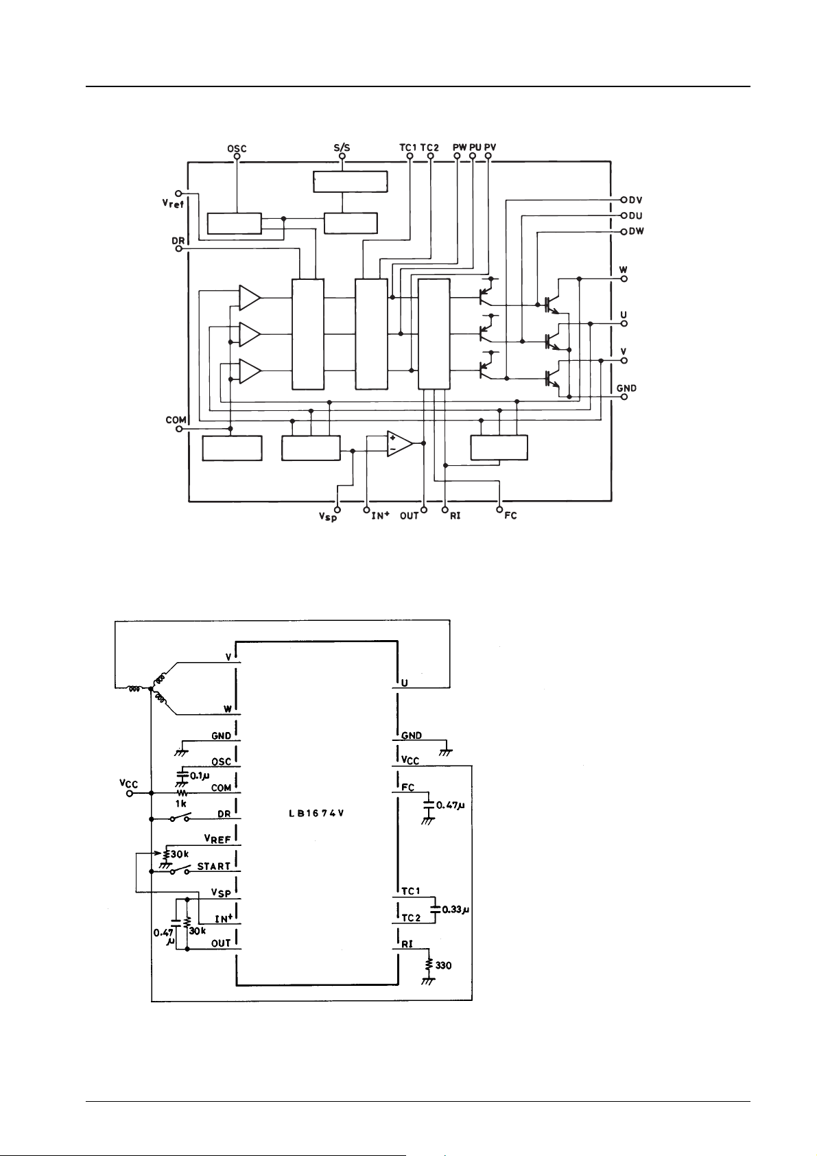
Equivalent Circuit Block Diagram
LB1674V
Supply bias
Oscillator
circuit
Commutation and
Start
detector
Speed
detector
Sample Application Circuits at V
Reference
voltage
starting logic
= 1.5 V
CC
Soft switch
Error
amplifier
Pre-driver
Current
detector
Note:
PU, PV and PW are internal
operation measurement pins.
Unit (resistance: Ω, capacitance: F)
No.4392-3/6
Page 4
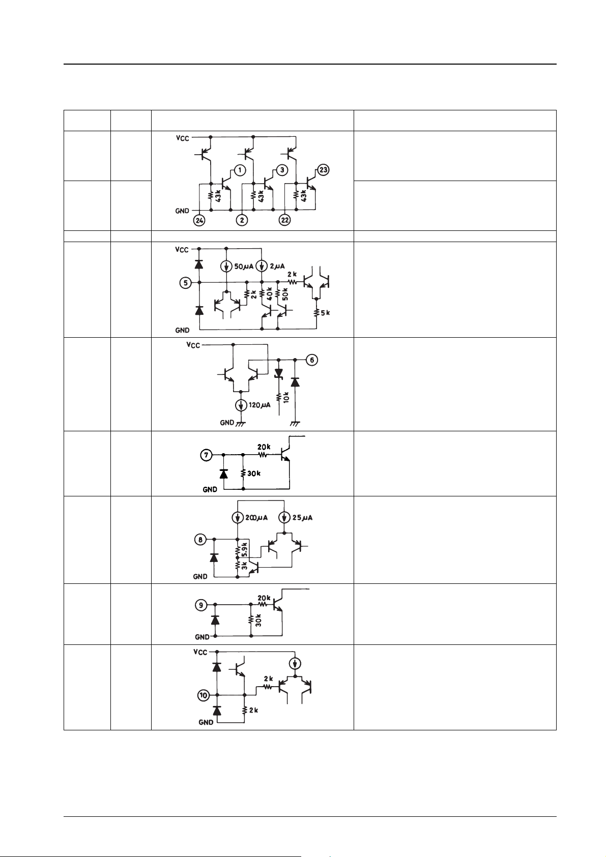
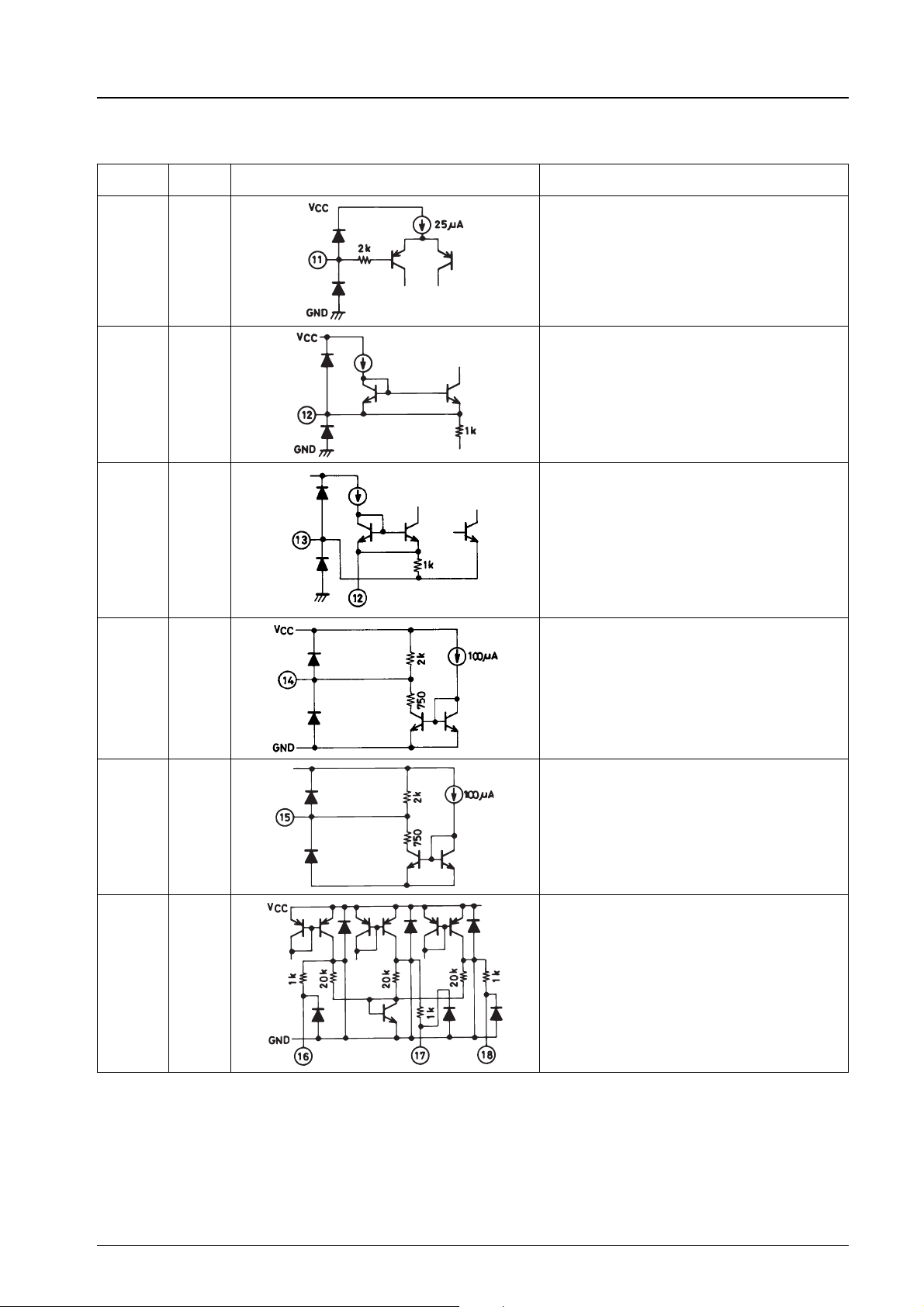
Pin Description
LB1674V
Unit (resistance: Ω)
Pin
Number
1
3
23
2
22
24
4 GND c Power and signal ground
5 OSC
6 COM*
Pin
Name
V
W
U
DW
DU
DV
Equivalent Circuit Description
c Motor coil connection pins
c Power transistor base pins
c Starting pulse period set pin
c Start-up waveform detection circuit offset set pin
7DR
8 Vref
9START
10 Vsp
cDrive direction switch pin (normally low)
c Reference voltage pin (0.5 V)
cStart/stop control pin.
Active-high
c Speed signal (motor induction voltage) detector
Continued on next page.
No.4392-4/6
Page 5
Continued from preceding page.
LB1674V
Unit (resistance: Ω)
Pin
Number
11 IN
12 OUT
13 RI
Pin
Name
+
Equivalent circuit Description
c Speed signal error amplifier reference input pin
c Speed signal error amplifier output for motor current
feedback
c Motor current detection pin
14 TC1
15 TC2
16
17
18
PW
PU
PV
c Motor current rising/falling time constant set pins
c Motor current rising/falling time constant set pins
c Current waveform generator.
Internal operation measurement pins. Must be left
open.
Continued on next page.
No.4392-5/6
Page 6

Continued from preceding page.
LB1674V
Unit (resistance: Ω)
Pin
Number
19 FC
20 V
21 GND c Power and signal ground
Pin
Name
CC
Equivalent circuit Description
c Abnormal oscillation stop pin
c Power supply
No products described or contained herein areintendedforuse in surgical implants, life-support systems, aerospace equipment,
nuclear power control systems, vehicles, disaster/crime-prevention equipment and the like, the failure of which may directly or
indirectly cause injury, death or property loss.
Anyone purchasing any products described or contained herein for an above-mentioned use shall:
1 Accept full responsibility and indemnify and defend SANYO ELECTRIC CO., LTD., its affiliates, subsidiaries and distributors
and all their officers and employees, jointly and severally, against any and all claims and litigation and all damages, cost and
expenses associated with such use:
2 Not impose any responsibility for any fault or negligence which may be cited in any such claim or litigation on SANYO
ELECTRIC CO., LTD., its affiliates, subsidiaries and distributors or any of their officers and employees jointly or severally.
Information (including circuit diagrams and circuit parameters) herein is for example only; it is not guaranteed for volume
production. SANYO believes information herein is accurate and reliable, but no guarantees are made or implied regarding its use
or any infringements of intellectual property rights or other rights of third parties.
This catalog provides information as ofAugust, 1996. Specifications and information herein are subject to change without notice.
No.4392-6/6
 Loading...