

Page 1
Ordering number: EN3513A
Monolithic Digital IC
LB1669, 1669M
2-Phase Unipolar Brushless Motor Driver
Overview
The LB1669, 1669M are 2-phase uniploar brushless motor
drivers. They make it possible to configure motor lock
protection and automatic recovery circuits with few extenal
components.
Features and Functions
.
Hall element direct connection possible
.
Output transistor with 1.5 A output current built in
.
Rotation detect function (Drive mode: ‘‘L’’, Stop mode:
‘‘H’’) built in
.
Motor lock protection and automatic recovery functions built
in
.
Thermal shutdown circuit built in
.
DIP-10S and MFP-10S packages mean small mounting
surfaces.
.
Pin compatible with LB1663, so can replace 12 V types.
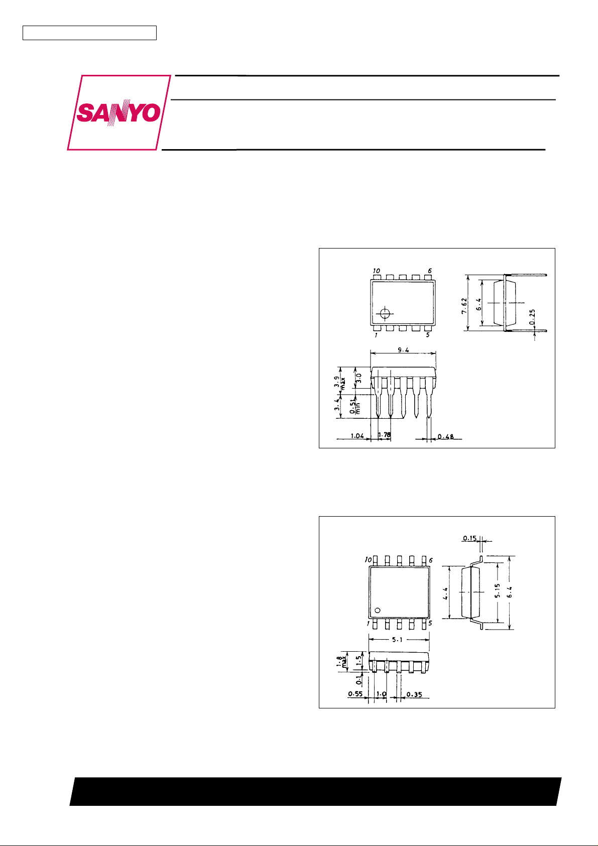
Package Dimensions
unit : mm
3098A-DIP10S
[LB1669]
SANYO : DIP10S
unit : mm
3086A-MFP10S
[LB1669M]
SANYO : MFP10S
SANYO Electric Co.,Ltd. Semiconductor Bussiness Headquarters
TOKYO OFFICE Tokyo Bldg., 1-10, 1 Chome, Ueno, Taito-ku, TOKYO, 110 JAPAN
D3096HA(II)/7120TA(GTPS) No.3513-1/5
Page 2
LB1669, 1669M
Specifications
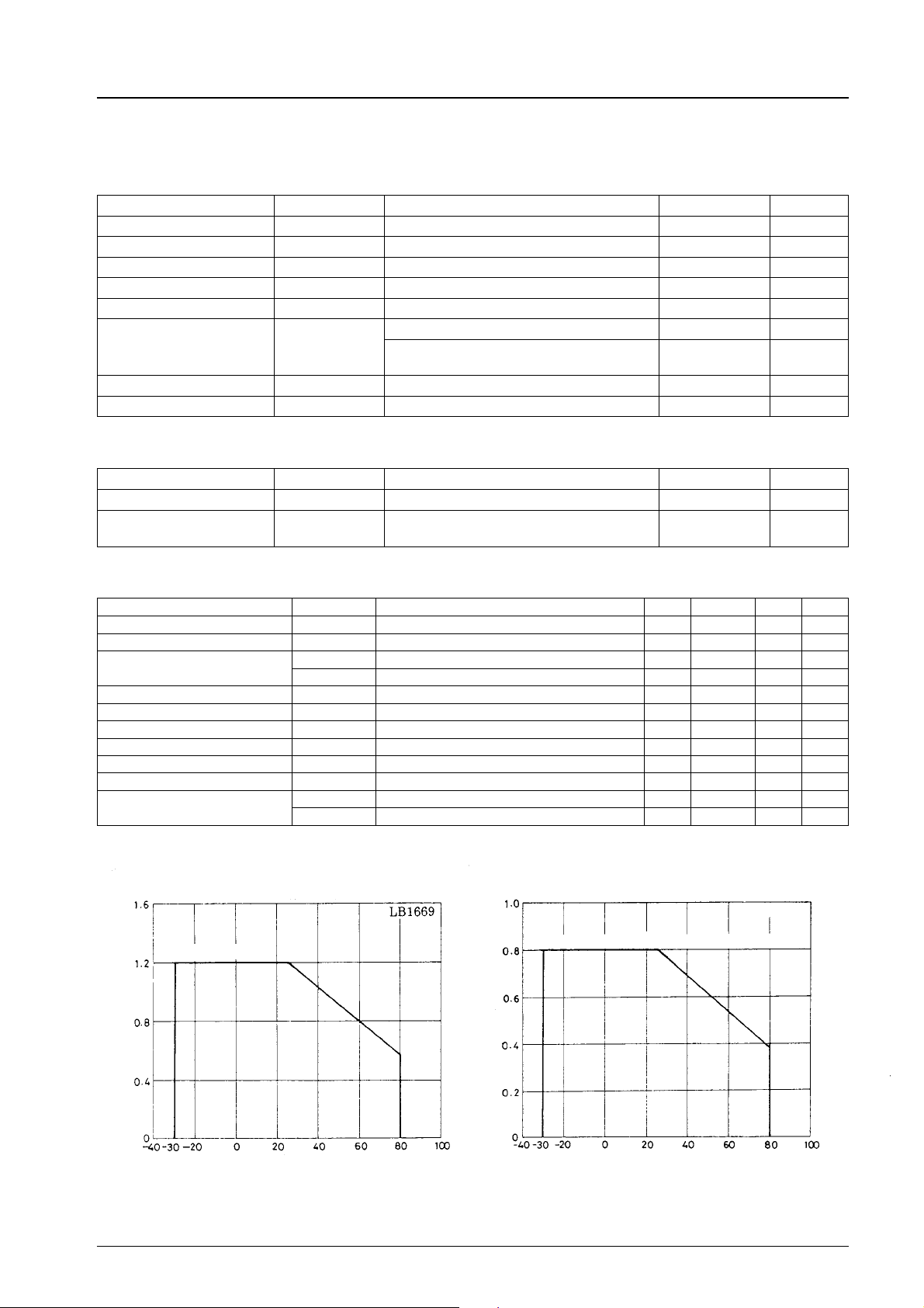
Absolute Maximum Ratings atTa=25°C
Parameter Symbol Conditions Ratings Unit
Maximum input current I
Output applied voltage V
Output current I
RD flow-in current I
RD applied voltage V
Allowable power dissipation Pd max
Operating temperature Topr –30 to +80
Storage temperature Tstg –55 to +125
Allowable Operating Conditions atTa=25°C
Parameter Symbol Conditions Ratings Unit
Input current range I
Common-mode input voltage
range
max t % 20 ms 200 mA
CC
–0.3 to +60 V
6.0 to 50 mA
0toVIN–1.5 V
OUT
V
OUT
RD
RD
CC
ICM
LB1669: Independent IC 1.2 W
LB 1669M: Mounted on 20 × 15 × 1.5 mm
glass epoxy board
3
1.5 A
10 mA
30 V
800 mW
°
°
C
C
Electrical Characteristics atTa=25°C, ICC=10mA
Parameter Symbol Conditions min typ max Unit
Output withstand voltage 1 V
Output withstand voltage 2 V
Output saturation voltage
V
voltage V
IN
Amp input offset voltage V
Amp input bias current I
RD output saturation voltage V
C flow-out current I
C discharge current I
Comparator input threshold
voltage
Pdmax–Ta Pdmax–Ta
Independent IC
OR
(sus) IO= 0.1 A 40 V
O
V
sat1 IO= 0.5 A 0.95 1.2 V
O
V
sat2 IO= 1.0 A 1.15 1.5 V
O
IN
OFF
BA
(sat) IRD= 5 mA 0.1 0.2 V
RD
C
C
V
TH
V
TH
ICC= 7.0 mA 6.4 6.7 7.0 V
1 2.1 3 3.9 µA
2 0.31 0.44 0.59 µA
1 0.77 0.8V
2 0.42 0.45V
60 V
–7 0 7.0 mV
–250 nA
0.83 V
IN
0.48 V
IN
LB1669M
Mounted on 20 × 15 × 1.5 mm3Glass epoxy board
Allowable power dissipation, Pd max – W
Ambient temperature, Ta – °C Ambient temperature, Ta – °C
Allowable power dissipation, Pd max – W
No.3513-2/5
Page 3
LB1669, 1669M
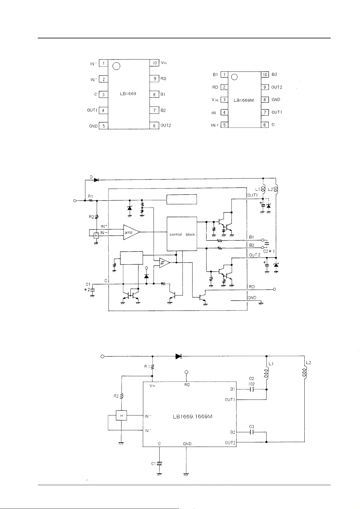
Pin Assignments
Top view Top view
Equivalent Circuit Block Diagram and Sample Application Circuit 1
V
IN
0.47 to 10 µ
Note * 1: If radio noise is a problem, 0.01 to 0.1µF
* 2: Use a low-leak capacitor.
Sample Application Circuit 2
Fixed
current
circuit
Thermal
shutdown
1to10µ
Unit (capacitance: F)
*
* C2 and C3 are ceramic
capacitors
If the output oscillates,
insert resistance in series
with the capacitor.
No.3513-3/5
Page 4
LB1669, 1669M
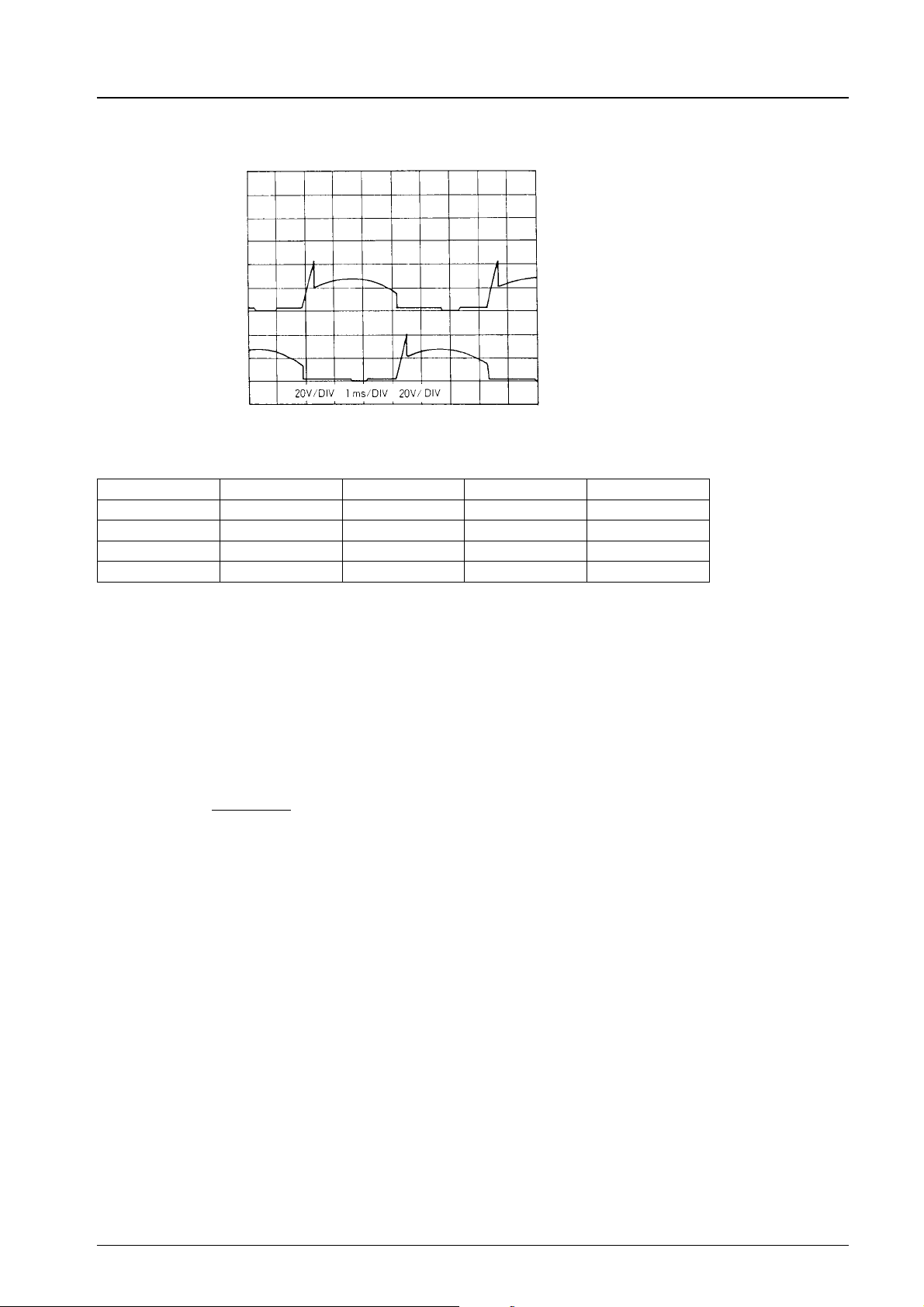
Sample Application Circuit 2 Output Waveform Diagram
Truth Table
IN+ IN– C OUT1 OUT2
HLLHL
LHLLH
HLHHH
LHHHH
Design Notes (See Sample Application Circuits.)
(1) Supply Voltage (VINpin)
The LB1669 series have the internal parallel regulator which supplies power to the Hall amplifier circuit and the control
block. Therefore, the driver ICs are not affected by power source fluctuations and kickbacks from the motor. They maintain
the stable operations even if noise signals such as surge are generated.
Set the resistance R1 between V
supply voltage range of a fan motor.
VINis 6.7 V typ at ICC= 7 mA.
The current flowing into V
V
=
CC–VIN
I
CC
.
Consideration given to surge voltage
IN
R1
The maximum allowable current at V
Vsurge = V
+R1×200mA......(2)
IN
(2) Hall input pin voltage (IN– and IN+ pins)
IN– and IN+ are input pins for the Hall element output. Set the Hall element output voltage to within the range of 0 V to V
– 1.5 V.
The gain between the Hall input pin and the output pin is 100 dB or greater. The offset voltage of the Hall input amplifier is
±7 mV therefore, the Hall element output must be set with the offset voltage (±7 mV) considered.
(3) Output transistors (OUT1 and OUT2 pins)
Output current I
= 1.5 A max.
O
Output saturation voltage V
The LB1669 requires one of the three types of output protection.
1 When external capacitors are connected between OUT and GND, the capacitance should not exceed 10 µF. Use
capacitance that will hold kickback voltage and back voltage to 60 V or less.
2 When external Zener diodes are connected, use one that will have a cutoff voltage of 40 V or less. If radio noise is a
problem, insert a capacitor of 0.01 to 0.1µF between B1 and B2.
3 When external capacitors are connected between OUT and B, use one that will hold kickback voltage to 40 V or less.
If it oscillates, insert resistance in series with the capacitor.
and VINso that the ICCcurrent of 6 mA to 50 mA can flow into the VINpin within the
CC
is calculated using the equation shown below.
.......(1)
pin is 200 mA, so the withstand voltage level is designed as follows.
IN
sat = 1.15 V/1.0 A (typ.)
O
IN
No.3513-4/5
Page 5
LB1669, 1669M
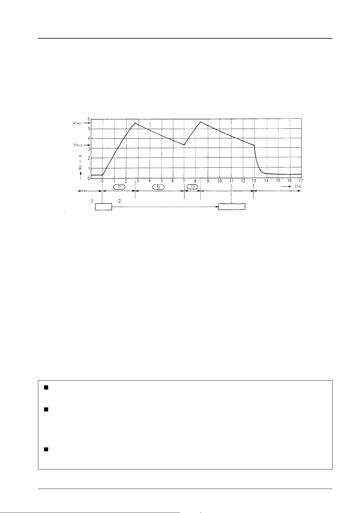
(4) Output protection function (C pin)
Capacitor pin used in forming an automatic recovery circuit. If rotation is stopped due to overload, the pin voltage level
increases and then forces the output to become inactive. In this case, after proper load adjustment, the output returns to the
‘drive’ mode from the ‘stop’ mode automatically. By changing the capacitor value, the lock detect time period can be set.
For 1 µF lock detection time about 2 seconds
lock protection time (output ON) about 1 second
(output OFF) about 6 seconds
Rotation
Output on Output off
Lock
Output on
Output off Rotation
Lock released
Automatic Recovery Circuit C Pin Voltage
1 When a fan is rotating, the capacitor is charged at 3 µA (typ) and discharged through the C with pulses according to the
rotational speed.
2 When a fan is locked, no discharge occurs through the C and the C voltage rises, turning OFF the output at 0.8 × V
3 When the output is turned OFF, discharge occurs through the C at 0.44 µA (typ). If the lock is not released when the C
voltage drops to V
These operations 2 and 3 are repeated at a cycle of approximately t
4 If the lock is released when the C voltage drops to V
2, the capacitor is charged to VTH1 again. (At this moment, the output is turned ON.)
TH
2, the output is turned ON, starting rotation.
TH
=1:6toprotect the motor.
on:toff
(5) Rotation detect signal (RD pin)
Open collector output (Drive mode: ‘‘L’’, Stop mode: ‘‘H’’)
(6) Radio noise reducing (pins B1 and B2)
These are the base pins for Darlington connected output transistors.
If radio noise is a problem, add a capacitor of 0.01 to 0.1µF or less.
(7) Thermal shutdown function
Shutdown the driver output in case of coil short-circuiting and abnormal IC heating.
.
IN
No products described or contained herein are intended for use in surgical implants, life-support systems, aerospace equipment,
nuclear power control systems, vehicles, disaster/crime-prevention equipment and the like, the failure of which may directly or
indirectly cause injury, death or property loss.
Anyone purchasing any products described or contained herein for an above-mentioned use shall:
1 Accept full responsibility and indemnify and defend SANYO ELECTRIC CO., LTD., its affiliates, subsidiaries and distributors
and all their officers and employees, jointly and severally, against any and all claims and litigation and all damages, cost and
expenses associated with such use:
2 Not impose any responsibility for any fault or negligence which may be cited in any such claim or litigation on SANYO
ELECTRIC CO., LTD., its affiliates, subsidiaries and distributors or any of their officers and employees jointly or severally.
Information (including circuit diagrams and circuit parameters) herein is for example only; it is not guaranteed for volume
production. SANYO believes information herein is accurate and reliable, but no guarantees are made or implied regarding its use
or any infringements of intellectual property rights or other rights of third parties.
This catalog provides information as of December, 1996. Specifications and information herein are subject to change without notice.
No.3513-5/5
 Loading...