

Page 1
LB1620
Ordering number : EN1210E
3-Phase DD Motor Driver
Monolithic Digital IC
SANYO Electric Co.,Ltd. Semiconductor Bussiness Headquarters
TOKYO OFFICE Tokyo Bldg., 1-10, 1 Chome, Ueno, Taito-ku, TOKYO, 110 JAPAN
O2097HA (KT)/8037KI/6115KI/7153KI/0252KI No.1210-1/6
Overview
The LB1620 is a 3-phase DD motor driver IC especially
suited for use in VCR capstan motor drive, drum motor
drive, and floppy disk motor drive applications.
Functions and Features
• 3-phase motor driver.
• Capable of controlling drive current.
• On-chip 3-phase control signal generator.
• Phase/speed control pin.
• Forward/reverse rotation control pin.
• Applicable to β/VHS, NTSC/PAL/SECAM.
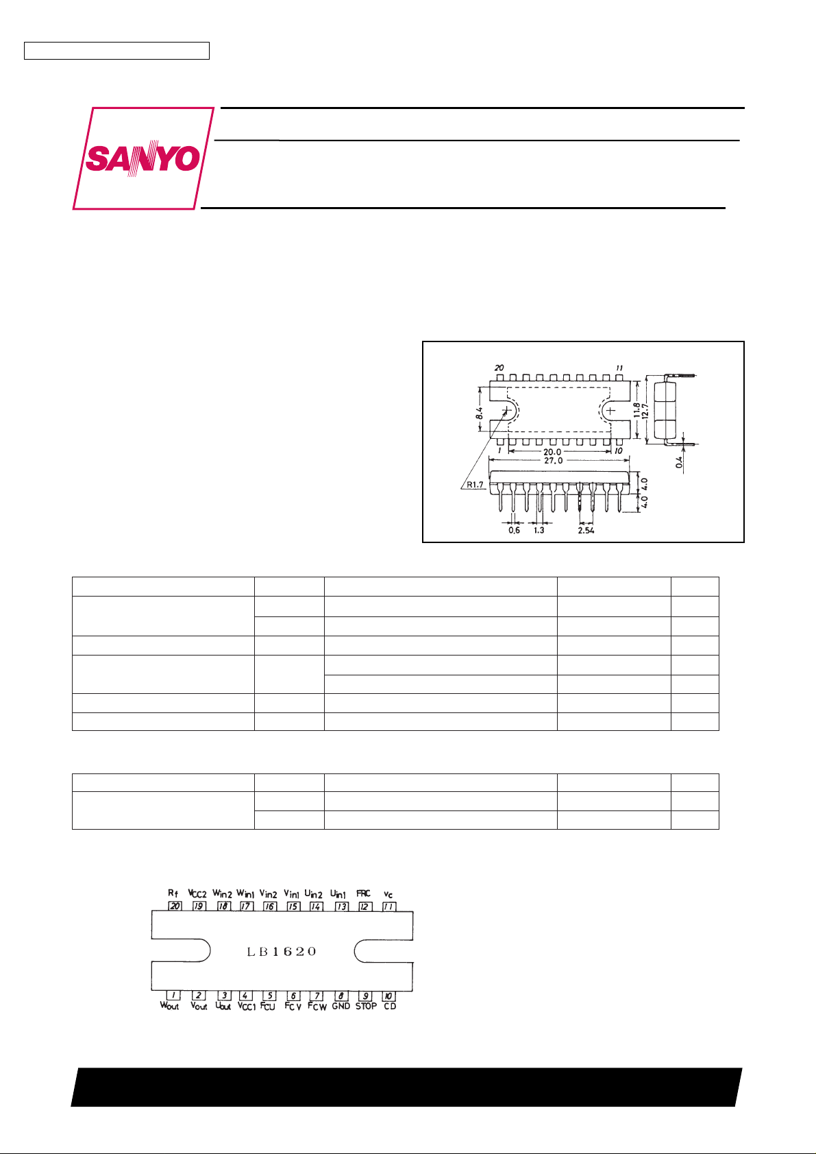
Package Dimensions
unit: mm
3037A-DIP20H
[LB1620]
SANYO : DIP20H
Specifications
Maximum Ratings
at Ta=25°C
Parameter Symbol Conditions Ratings Unit
Maximum supply voltage V
CC
128V
V
CC
214V
Maximum load current I
L
1.5 A
Allowable power dissipation Pd max Ideal heat dissipation 15 W
Without heat sink 3 W
Operating temperature Topr –20 to +75 °C
Storage temperature Tstg –55 to +150 °C
Allowable Operating Condition at Ta=25°C
Parameter Symbol Conditions Ratings Unit
Supply voltage V
CC
1 8.5 to 26.4 V
V
CC
2 8.5 to 14.0 V
Pin Assignment
Top view
Page 2
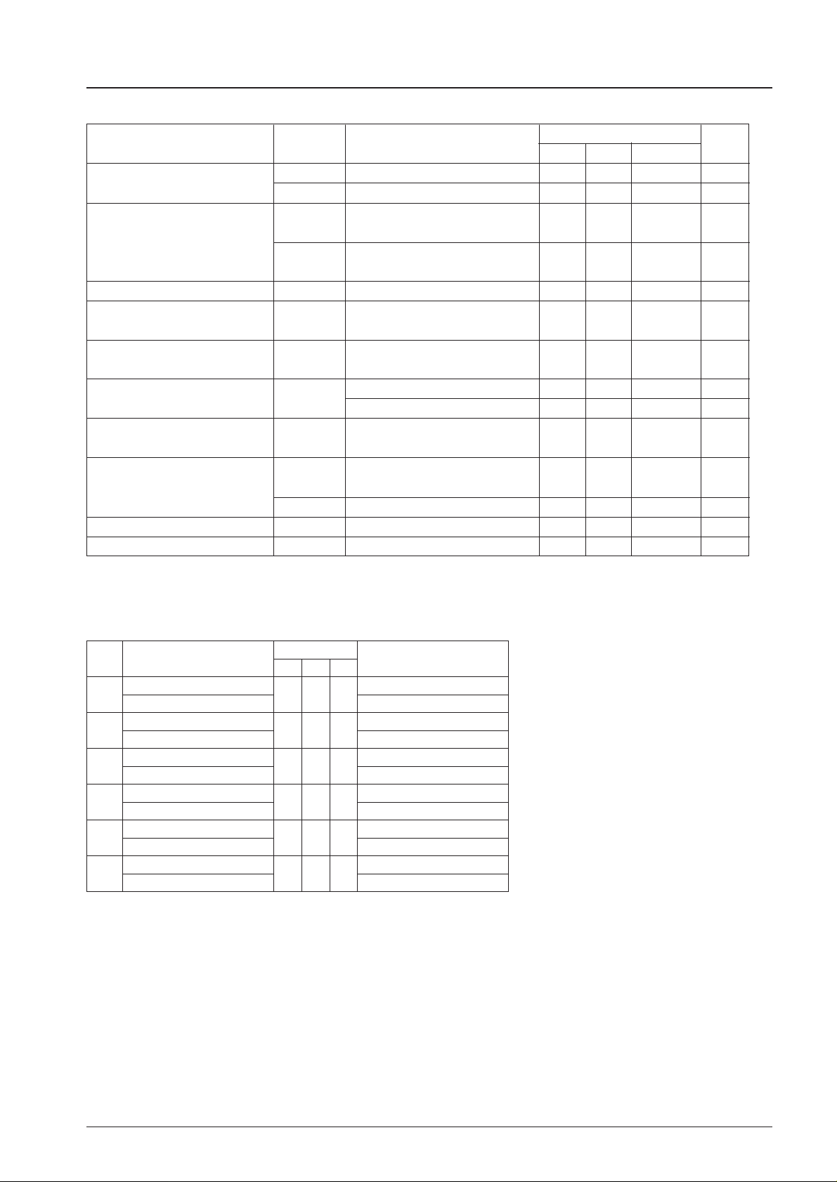
Electrical Characteristics at Ta=25°C, V
CC
1=12V, VCC2=9V
Parameter Symbol Conditions
Ratings
min typ max
Unit
Current drain I
CC
off Vc=0V, Vstop=2V, ICC1+ICC2 12 18 mA
I
CC
dri Vc=7V, Vstop=2V, ICC1+ICC2 22 40 mA
Saturation voltage V
O
(sat)1 IO=0.58A, VCC1=9.6V, 2.1 V
V
O
sink+VOsource
V
O
(sat)2 IO=1A, VCC1=18V, 5.0 V
V
O
sink+VOsource
In-phase voltage range 2.0 V
CC
2–2.5 V
Motor forward rotation 2.0 V
CC
2 V
input voltage range
Motor reverse rotation 0 0.3 V
input voltage range
Interphase current variation Driver stage –25 0 +25 %
Output stage –25 0 +25 %
Speed control voltage (off) Vc1 R
f
=0Ω, Rs=0Ω, 4.0 V
FC pin
→GND current=5µA
Speed control voltage (on) Vc2 R
f
=0Ω, Rs=0Ω, 4.5 V
FC pin
→GND current=0.5mA
Vc3 R
f
=1Ω, Rs=100Ω, VRf=100mV 4.6 V
Closed loop voltage gain R
f
=1Ω, Rs=100Ω, IL=100mA 0.44 A/V
Input sensitivity 20 mV
LB1620 Truth Table
LB1620
No.1210-2/6
W phase → V phase
V phase → W phase
L
H
1
Source
Sink
Forward/Reverse
Control (FRC)
Input
U
H H L
W phase → U phase
U phase → W phase
L
H
2 H L L
V phase → W phase
W phase → V phase
L
H
3 L L H
U phase → V phase
V phase → U phase
L
H
4 L H L
V phase → U phase
U phase → V phase
L
H
5 H L H
U phase → W phase
W phase → U phase
L
H
6 L H H
V W
Input : "H" : Each phase input (1) is more than 0.2V higher than each phase input (2).
"L" : Each phase input (1) is more than 0.2V lower than each phase input (2).
Forward/reverse control : "H" : 2.0 to VCC2
: "L" : 0 to 0.3V
Page 3
LB1620
No.1210-3/6
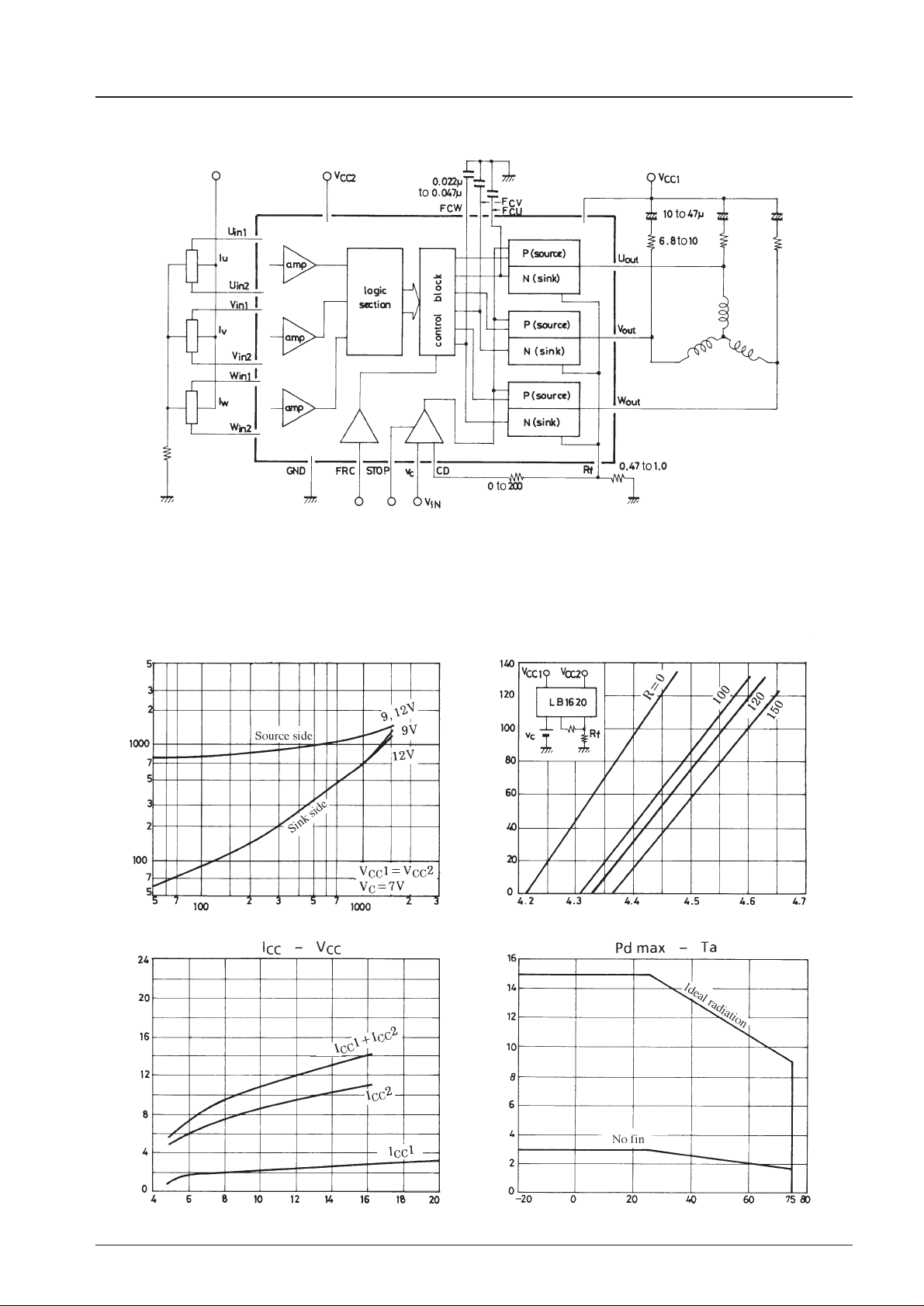
Equivalent Circuit Block Diagram and Peripheral Circuit
Forward/reverse control
Output collector current, ICO– mA
Saturation voltage – mV
Supply voltage, VCC– V
Quiescent current, I
CC
– mA
Ambient temperature, Ta – °C
Allowable power dissipation, Pd max – W
Saturation Voltage – I
CO
Control voltage, VC– V
R
f
pin voltage – mV
RfPin Voltage – V
C
Feedback resistor
Unit (resistance : Ω, capacitance : F)
Page 4
LB1620
No.1210-4/6
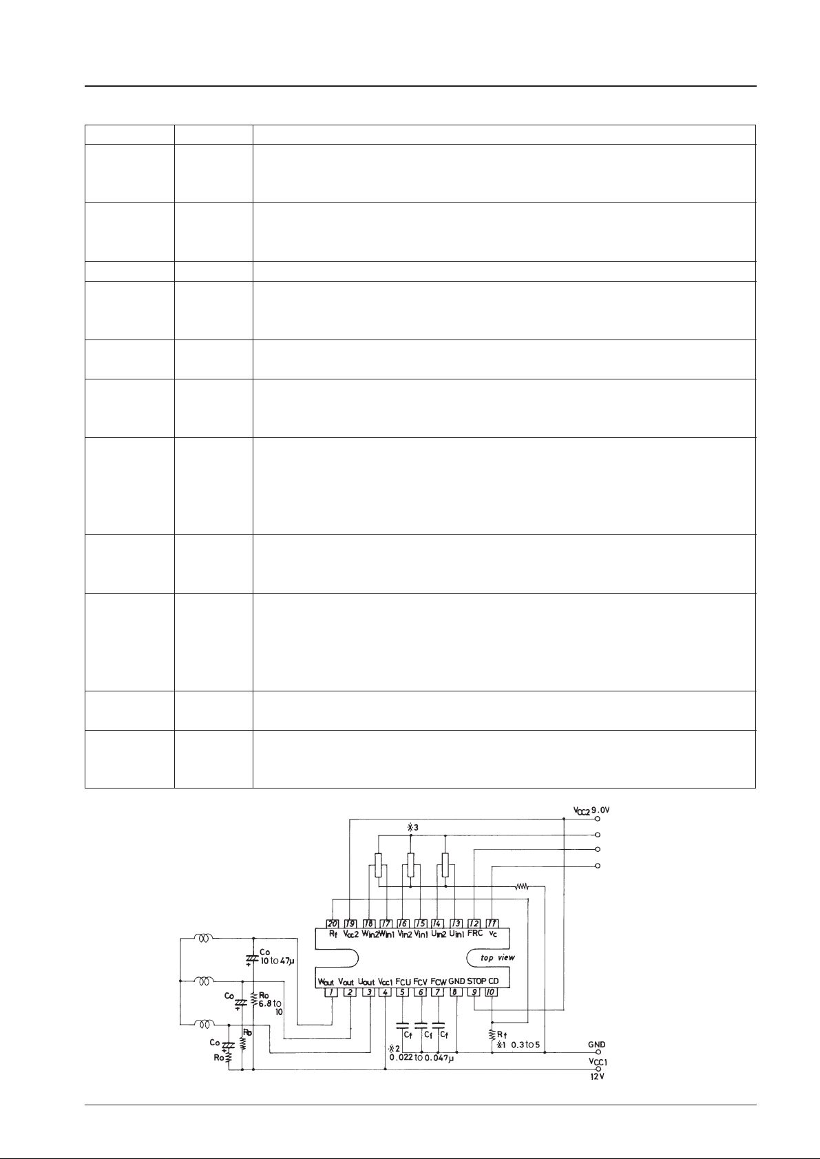
Pin Description
Pin name Pin No. Function
UIN1, UIN2
VIN1, VIN2
WIN1, WIN2
13, 14
15, 16
17, 18
U phase Hall element input pin, "H" of logic : VIN1>VIN2
V phase Hall element input pin, "H" of logic : VIN1>VIN2
W phase Hall element input pin, "H" of logic : VIN1>VIN2
U
OUT
V
OUT
W
OUT
3
2
1
U phase output pin
V phase output pin
W phase output pin
VCC1
4 Power supply pin for applying output
VCC2
19
Power supply pin for applying voltage to each section other than output section.
The control point of control voltage is at approximately 1/2 of this voltage.
This voltage must be stabilized to be free from ripple, noise, etc.
R
f
20
Output current detect pin. By connecting Rfacross this pin and GND pin, output
current is detected as voltage.
C
D
10
Pin for fetching current (voltage) detected with Rf.
By connecting a resistor across CDpin and Rf, speed control start voltage can be
fine-adjusted.
STOP 9
Overcurrent protection pin.
Voltage being lower than that on CDpin is taken to be identical to overcurrent
flow, causing output to be cut off. Off-state is held.
For example, if STOP pin is set to 1.5V for Rf=1Ω, approximately 1.5A or more
flows at output, causing output to be cut off.
F
CU
F
CV
F
CW
5
6
7
Frequency characteristic compensation pin.
Closed loop oscillation in current-controlled system (including motor, F/V
converter) is stopped.
V
C
11
Speed/phase control pin.
Control starts at approximately 1/2 of VCC2.
Control is of current-controlled type that controls output current.
For Rf=1Ω, LB1620 closed loop has gm of 0.44A/V typ, which can be adjusted by
varying Rf.
GND 8
GND for other than output.
Minimun potential of output transistor is at Rfpin.
F/RC 12
Forward/reverse rotation control pin.
By setting this pin to "H" (more than 2V) / "L" (less than 0.3V), truth value is
changed to perform forward/reverse rotation.
Sample Application Circuit
Unit (resistance : Ω, capacitance : F)
(Stabilization)
Power supply for Hall element
Forward/reverse select
Control signal input 2
Page 5
LB1620
No.1210-5/6
Notes on Sample Application Circuit
*1. Rfis determined by starting torque required for coil impedance F/V conversion voltage (control input). Rfshould be
0.3Ω to 5Ω.
*2. Cfis for stopping oscillation and is determined by motor characteristic and F/V converter-included closed loop
characteristic. Cfshould be 0.022µF to 0.047µF.
*3. For how to connect Hall element, either parallel connection or series connection is available as long as input voltage
is within the range specified.
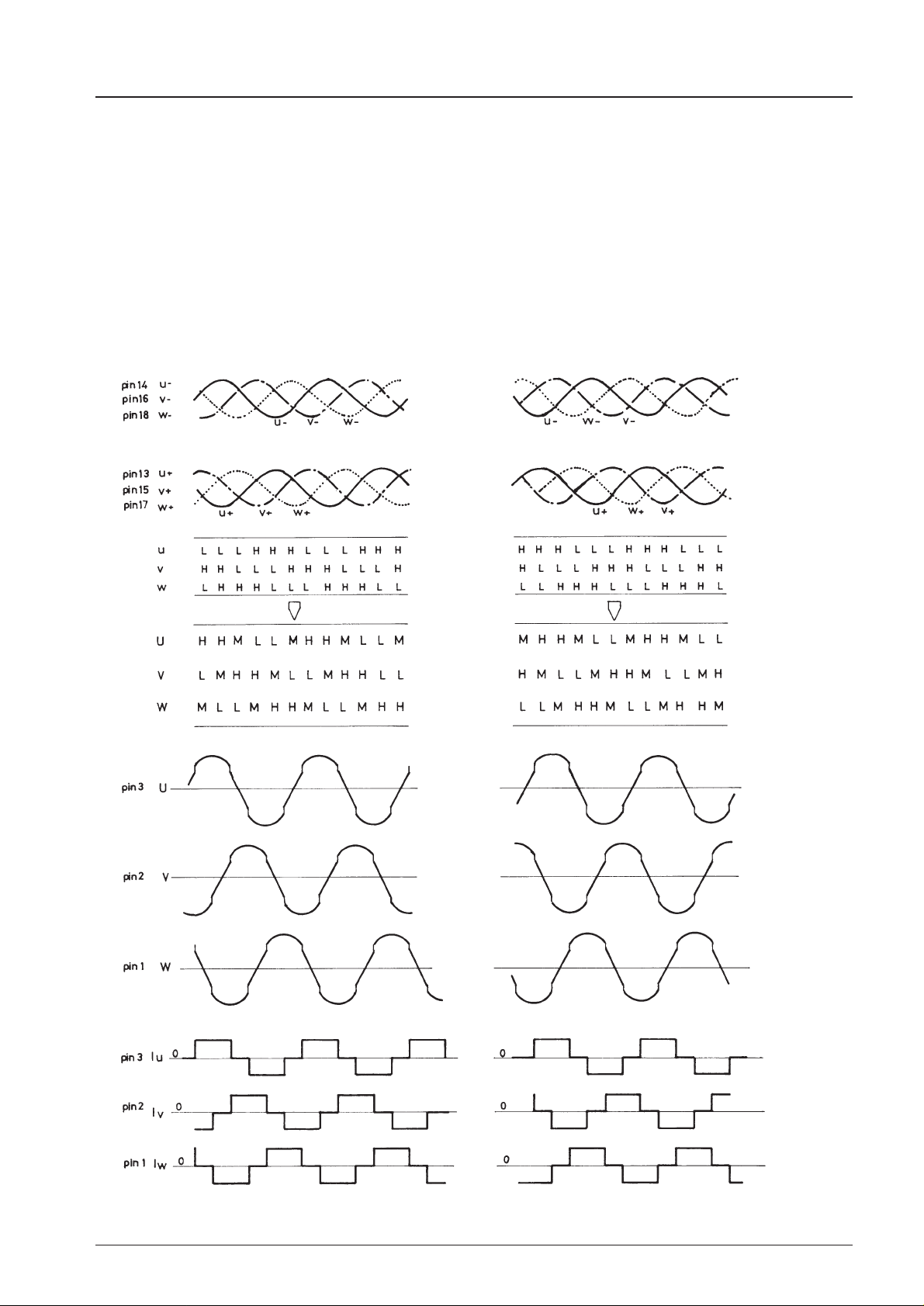
Timing Chart
Forward/reverse control "L" pin 12 Forward/reverse control "H" pin 12
From truth table From truth table
Page 6
LB1620
No.1210-6/6
No products described or contained herein are intended for use in surgical implants, life-support systems,
aerospace equipment, nuclear power control systems, vehicles, disaster/crime-prevention equipment and
the like, the failure of which may directly or indirectly cause injury, death or property lose.
Anyone purchasing any products described or contained herein for an above-mentioned use shall:
Accept full responsibility and indemnify and defend SANYO ELECTRIC CO., LTD., its affiliates,
subsidiaries and distributors and all their officers and employees, jointly and severally, against any
and all claims and litigation and all damages, cost and expenses associated with such use:
Not impose any responsibilty for any fault or negligence which may be cited in any such claim or
litigation on SANYO ELECTRIC CO., LTD., its affiliates, subsidiaries and distributors or any of
their officers and employees jointly or severally.
Information (including circuit diagrams and circuit parameters) herein is for example only; it is not guaranteed for volume production. SANYO believes information herein is accurate and reliable, but no guarantees
are made or implied regarding its use or any infringements of intellectual property rights or other rights of
third parties.
This catalog provides information as of October, 1997. Specifications and information herein are subject
to change without notice.
 Loading...