

Page 1
Ordering number: EN1218C
Monolithic Digital IC
LB1412
Level Meter Driver for 12 LEDs
Functions and Features
.
Bar-shaped display of input level by means of 12 LEDs
.
High-order 5 dots with peak hold
.
Built-in oscillator for peak hold reset. Requires 1 pce. each
of external C, R. Uses either oscillator at the time of stereo
operation. Capable of also resetting manually.
.
Capable of constant-current driving low-order 7 dots (green
LED). Constant-current value variable with an external
resistor
.
Lower current drain available by connecting green LEDs in
series
.
Built-in input amplifier
.
Requires no other light-up level adjustment than adjustment
for 0 dB. D1 error: within ±3dBof20dB
.
Supply voltage range : 10 to 16 V
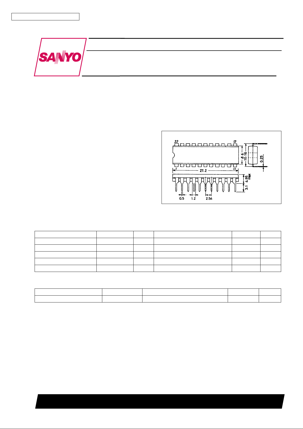
Package Dimensions
unit : mm
3010A-DIP22
[LB1412]
SANYO : DIP22
Specifications
Absolute Maximum Ratings at Ta = 25°C
Parameter Symbol Pin No. Conditions Ratings Unit
Maximum supply voltage V
Output current I
Allowable power dissipation Pd max Ta = 60°C 650 mW
Operating temperature Topr −30 to +75 °C
Storage temperature Tstg −40 to +125 °C
max 15 −0.3 to+18 V
CC
OL
1 to 5 D8 to D12, output on 30 mA
Allowable Operating Range at Ta = 25°C
Parameter Symbol Conditions Ratings Unit
Supply voltage V
CC
10 to 16 V
SANYO Electric Co.,Ltd. Semiconductor Bussiness Headquarters
TOKYO OFFICE Tokyo Bldg., 1-10, 1 Chome, Ueno, Taito-ku, TOKYO, 110 JAPAN
53096HA(II)/9097KI/8075MW/113KI(KOT) No.1218-1/5
Page 2

LB1412
Electrical Characteristics at Ta = 25°C, VCC=12V
Parameter Symbols Pin No. Conditions min typ max Unit
Input bias current Amp (1) I
Output saturation
voltage
Amp (1) V
Amp (1) V
Voltage gain Amp (1) V
Input resistance Amp (2) R
Load resistance Amp (2) R
Output current Amp (2) I
Voltage gain Amp (2) V
Output current I
Output saturation voltage
Output leak current
D8 V
D1 G
D2 G
D3 G
D4 G
Comparator level
D5 G
D6 G
D7 G
D9 G
D10 G
D11 G
D12 G
Reference voltage V
R pin flow-out current I
R pin voltage V
Oscillation frequency f
Current drain I
BIN1
OH01
OL01
GA1
IN2
02
OL02
GA2
OL
V
sat
V
sat
l
off
l
off
THD8
D1
D2
D3
D4
D5
D6
D7
D9
D10
D11
D12
Z
OLR
R
OSC
CC
7 −3 −0.2 0 µA
8 Pins 8, 9 short 10.5 11.2 11.6 V
8 Pins 8, 9 short 1.0 1.5 2.0 V
9 8 12 16 kΩ
10 35 50 65 kΩ
10 3 6 12 mA
19,22 D1,D5:3kΩacross VZand I
17, 18,
19, 21,
D2 to D4, D6 to D7 : Output
Transistor on across V
22
1 to 5 D8 to D12 : I
19, 22 D1, D5 : output transistor off 0 30 µA
1 to 15 D8 to D12 : output transistor off 0 30 µA
D8 : Voltage to turn on D8 by
1
applying DC voltage across VZand
I
NZ
16 D8 light-up level:0dB −23 −20 −17 dB
17 D8 light-up level:0dB −17 −15 −13 dB
18 D8 light-up level:0dB −12 −10 −8 dB
19 D8 light-up level:0dB −8 −7 −6 dB
20 D8 light-up level:0dB −6 −5 −4 dB
21 D8 light-up level:0dB −4 −3 −2 dB
22 D8 light-up level:0dB −1.5 −1 −0.5 dB
2 D8 light-up level:0dB 0.5 1 1.5 dB
3 D8 light-up level:0dB 2 3 4 dB
4 D8 light-up level:0dB 4 5 6 dB
5 D8 light-up level:0dB 7 8 9 dB
12 3 kΩ across VZand I
11 VR= 0 V, OSC pin: open −0.6 −0.3 −0.1 mA
11 OSC pin: open 0.4 0.7 0.9 V
13 1 MΩ, 2.2 µF across VCCand V
3kΩacross V
15
outputs off
OLD1 to D5
and I
Z
30 100 dB
1.8 2.0 2.2 times
13 17 20 mA
1.0 1.3 V
Z
and I
LED
LED
= 30 mA 1.5 2.0 V
−0.625 −0.55 −0.465 V
LED
LED
Z
, all D
5.6 6.3 6.8 V
1.5 2 2.5 s
915mA
Allowable power dissipation, Pd max – mW
Pd max – Ta
Ambient temperature, Ta – °C
No.1218-2/5
Page 3
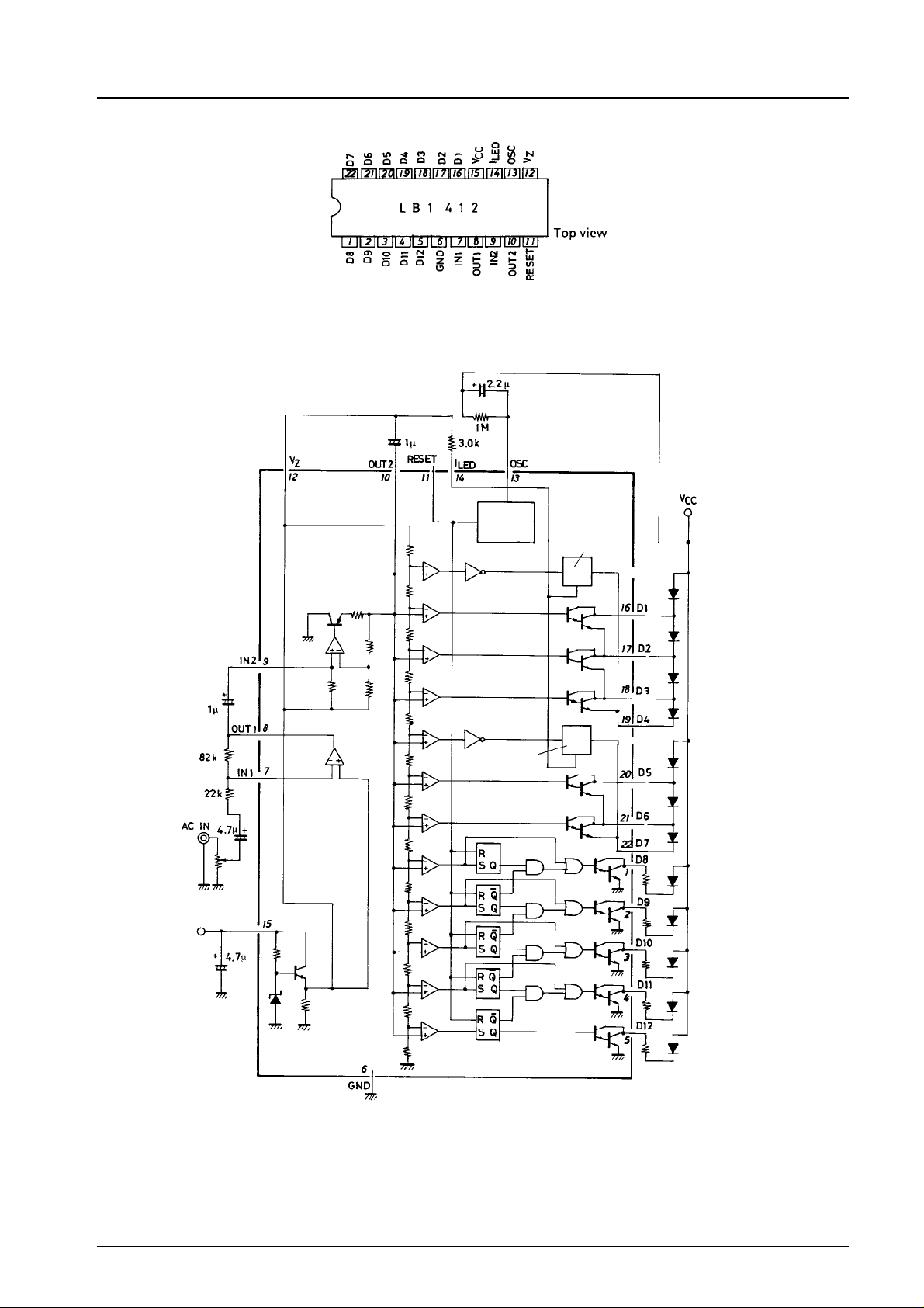
Pin Assignment
Equivalent Circuit Block Diagram
LB1412
V
CC
10 to 16 V
Oscillator
Constantcurrent driver
Constantcurrent driver
Unit (resistance: Ω, capacitance: F)
No.1218-3/5
Page 4
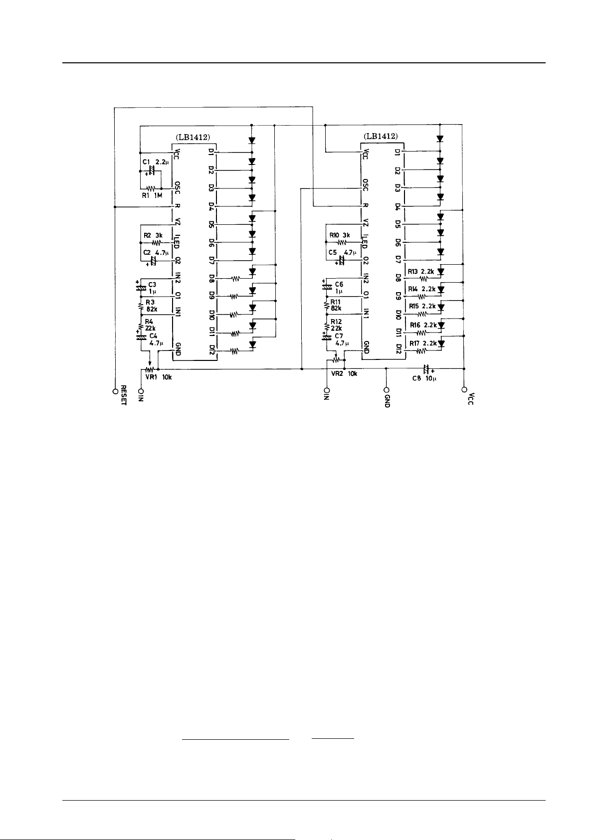
Sample Application Circuit
LB1412
R5 2.2 k
R6 2.2 k
R7 2.2 k
R8 2.2 k
R9 2.2 k
Note : Input signal of approximately 110 mVrms causes D8 (0 dB display) to light.
For sample application circuit:
1. The LB1412 consists of the following blocks.
.
Input amp 1 : Amplification of input signal, variable with external constants
.
Input amp 2 : Amplification of signal (fixed, double), detection of signal
.
Reference voltage : Reference voltage of comparator, constant-current drive of LED
.
Comparator : Comparison of input voltage
.
LED driver : LED drive, D1 to D7 : Constant-current drive
.
Peak hold circuit : Hold of highest-order point of high-order 5 points (D8 to D12)
.
Oscillator for peak hold reset : Peak hold circuit reset
2. Description of constants of each block
2-1 R3, R4 (R11, R12)
The gain of amp 1 depends on R3, R4. Gain of amp 1 = R3/R4 times. The gain of amp 1 must not exceed 4 times
(12 dB).
R3+R46100 kΩ (C4 = 4.7 µF)
2-2 C2, C3 (C5, C6)
C3 is for coupling amp 1 with amp 2 and its value is 1 µF. C2 is for controlling the time to turn off LED.
2-3 R2 (R10)
The current of LEDs connected to D1 to D7 depends on R2. The current is stabilized to be approximately 17 mA at R2
=3kΩand approximately 11 mA at R2 = 4.7 kΩ.
2-4 R5 to R9 (R13 to R17)
The current of LEDs connected to D8 to D12 depends on these resistors. D8 to D12 pins are collectors of Darlington
transistors.
I
D8 to D12
=
VCC–V
sat D8 to D12–VFLED
R5 to 9
V
– 3.5 V
CC
6
R5 to 9
10 to 16 V
Unit (resistance: Ω, capacitance: F)
I
D8 to D12
is approximately 4 mA at R5 to 9 = 2.2 kΩ
No.1218-4/5
Page 5
LB1412
2-5 Reset pin (Pin 11)
When the reset pin is open, peak hold of D8 to D12 occurs. When the reset pin is connected to GND, reset occurs.
Connecting the reset pin to GND causes no peak hold.
2-6 C1, R1
The oscillation cycle of oscillator depends on the product of C1 and R1. The oscillation cycle at C1 = 2.2 µF, R1 =
1MΩis approximately 2 seconds. However, if an electrolytic capacitor is used for C1, the actual capacitance differs
from the marked value.
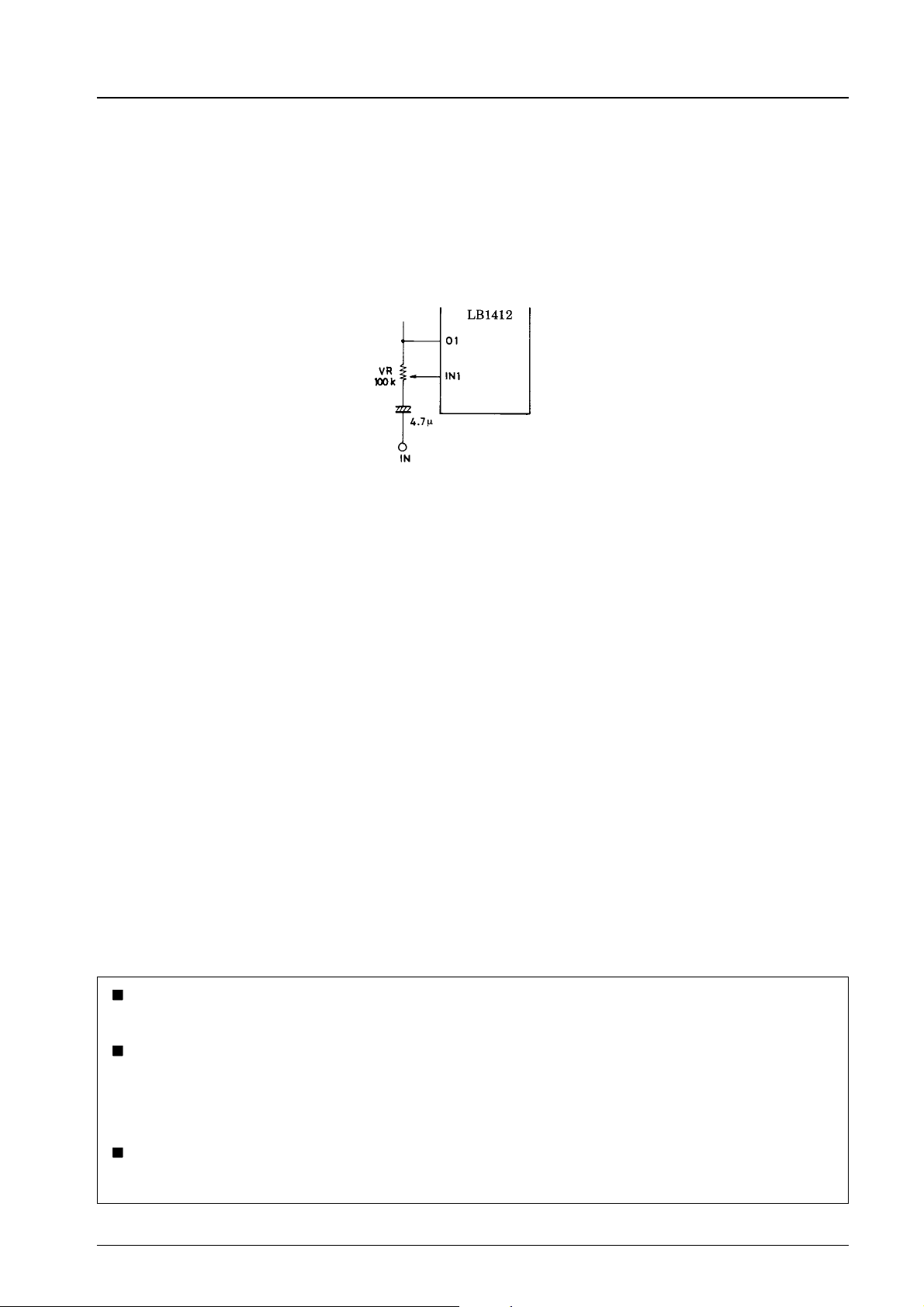
2-7 Reduction in number of parts
R3, R4, VR1 are substituted by one VR.
Unit (resistance: Ω, capacitance: F)
No products described or contained herein are intended for use in surgical implants, life-support systems, aerospace equipment,
nuclear power control systems, vehicles, disaster/crime-prevention equipment and the like, the failure of which may directly or
indirectly cause injury, death or property loss.
Anyone purchasing any products described or contained herein for an above-mentioned use shall:
1 Accept full responsibility and indemnify and defend SANYO ELECTRIC CO., LTD., its affiliates, subsidiaries and distributors
and all their officers and employees, jointly and severally, against any and all claims and litigation and all damages, cost and
expenses associated with such use:
2 Not impose any responsibility for any fault or negligence which may be cited in any such claim or litigation on SANYO
ELECTRIC CO., LTD., its affiliates, subsidiaries and distributors or any of their officers and employees jointly or severally.
Information (including circuit diagrams and circuit parameters) herein is for example only; it is not guaranteed for volume
production. SANYO believes information herein is accurate andreliable, but no guarantees are made or impliedregarding its use
or any infringements of intellectual property rights or other rights of third parties.
This catalog provides information as of May, 1996. Specifications and information herein are subject to change without notice.
No.1218-5/5
 Loading...