

Page 1
Ordering number : ENN6216A
LB11990W
Three-Phase Brushless Motor Driver
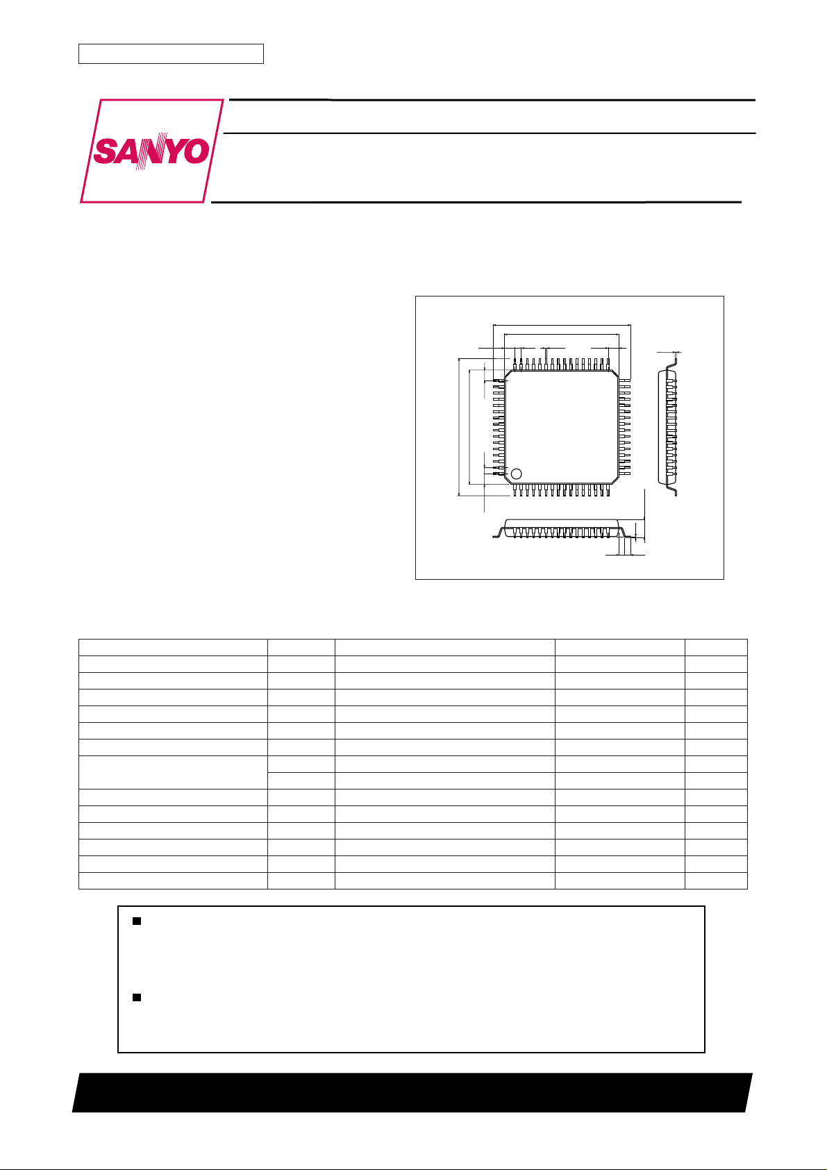
Package Dimensions
unit: mm
3190-SQFP64
1.25 0.5 1.250.18
48
49
1.25
10.0
12.0
[LB11990W]
12.0
10.0
Monolithic Digital IC
LB11990W
0.15
33
32
0.5
17
16
1.7max
0.1
0.5
0.5
SANYO : SQFP64
1.25
64
1
Specifications
Absolute Maximum Ratings at Ta = 25°C
Parameter Symbol Conditions Ratings Unit
Maximum supply voltage 1 VCC1 max 7 V
Maximum supply voltage 2 VCC2 max 8.5 V
Maximum supply voltage 3 VS_C max Capstan motor driver 7.0 V
Maximum supply voltage 4 VS_D max Drum motor driver 7.0 V
Maximum supply voltage 5 VS_L max Loading motor driver 7.0 V
Applied output voltage Vo max 8.0 V
Applied input voltage VI1 max Control circuits –0.3 to VCC1 + 0.3 V
VI2 max U, V, W, COM 8.0 V
Capstan motor output current IOC max 1.0 A
Drum motor output current IOD max 1.0 A
Loading motor output current IOL max 0.6 A
Allowable power dissipation Pd max IC only 0.6 W
Operating temperature Topr –20 to +75 °C
Storage temperature Tstg –55 to +150 °C
Any and all SANYO products described or contained herein do not have specifications that can handle
applications that require extremely high levels of reliability, such as life-support systems, aircraft's
control systems, or other applications whose failure can be reasonably expected to result in serious
physical and/or material damage. Consult with your SANYO representative nearest you before using
any SANYO products described or contained herein in such applications.
SANYO assumes no responsibility for equipment failures that result from using products at values that
exceed, even momentarily, rated values (such as maximum ratings, operating condition ranges, or other
parameters) listed in products specifications of any and all SANYO products described or contained
herein.
SANYO Electric Co.,Ltd. Semiconductor Company
TOKYO OFFICE Tokyo Bldg., 1-10, 1 Chome, Ueno, Taito-ku, TOKYO, 110-8534 JAPAN
N0199RM(KI)
No. 6216-1/14
Page 2
LB11990W
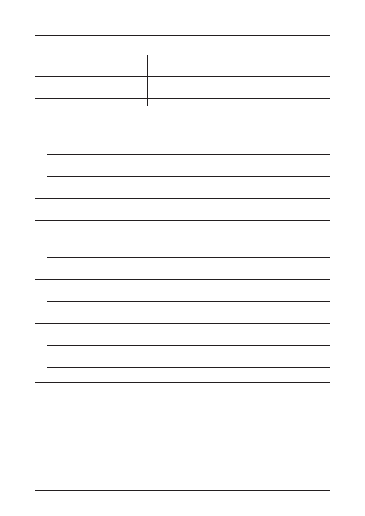
Allowable Operating Ranges at Ta = 25°C
Parameter Symbol Conditions Ratings Unit
Power supply voltage 1 VCC1VCC1 ≤ VCC2 2.7 to 6.0 V
Power supply voltage 2 VCC2 3.5 to 8.5 V
Power supply voltage 3 VS_C VS_C ≤ VCC2 to 7.0 V
Power supply voltage 4 VS_D VS_D ≤ VCC2 to 7.0 V
Power supply voltage 5 VS_L VS_L ≤ VCC2 2.2 to 7.0 V
Hall input amplitude VHALL Capstan motor ±20 to ±80 mVp–p
Electrical Characteristics/Capstan Motor Driver Block at Ta = 25˚C, VCC1 = 3V, VCC2 = 4.75V, VS = 1.5V
Parameter Symbol Conditions
Vcc1 power supply current Icc1 Iout = 100 mA VSTBY_C = 3V 4 8 mA
Vcc2 power supply current Icc2 Iout = 100 mA VSTBY_C = 3V 6 12 mA
Vcc1 idle current Icc1Q VSTBY_C = 0V 2.1 4 mA
Vcc2 idle current Icc2Q VSTBY_C = 0V 100 µA
Vs idle current IsQ VSTBY_C = 0V 75 100 µA
Power supply current
Upper side residual voltage VXH1 Iout = 0.2A 0.15 0.22 0.29 V
VX1VX2
Lower side residual voltage VXL1 Iout = 0.2A 0.15 0.20 0.25 V
Upper side residual voltage VXH2 Iout = 0.5A 0.25 0.40 V
Lower side residual voltage VXL2 Iout = 0.5A 0.25 0.40 V
Output saturation voltage Vosat Iout = 0.8A, Sink + Source 1.40 V
Overlap amount O.L RL = 39Ω × 3, Rangle = 20 kΩ Note 2 73 80 87 %
Input offset voltage VHOFF Note 1 Design target value –5 +5 mV
Common mode input range VHCM Rangle = 20 kΩ 0.95 2.1 V
Input/output voltage gain VGVH Rangle = 20 kΩ 24.5 27.5 30.5 dB
Hall amplifier
High level voltage VSTH 2.5 VCC1V
Low level voltage VSTL –0.2 +0.7 V
Input current ISTIN VSTBY_C = 3V 50 µA
Leakage current ISTLK VSTBY_C = 0V –30 µA
Standby pinFRC pinVH
High level voltage VFRCH 2.5 VCC1V
Low level voltage VFRCL –0.2 +0.4 V
Input current IFRCIN VFRC_C = 3V 20 30 µA
Leakage current IFRCLK VFRC_C = 0V –30 µA
Hall power supply voltage VHALL IH = 5 mA, VH(+) – VH(–) 0.75 0.85 0.95 V
(–) pin voltage VH(–) IH = 5 mA 0.81 0.88 0.95 V
Input offset voltage VFGOFF –3 +3 mV
Input bias current IbFG VFGIN+ = VFGIN– = 1.5V 500 nA
Input bias current offset ∆IbFG VFGIN+ = VFGIN– = 1.5V –100 +100 nA
Common mode input range VFGCM 1.2 2.5 V
High level output voltage VFGOH With internal pull-up 2.8 V
Low level output voltage VFGOL With internal pull-up 0.2 V
FG comparator
Voltage gain VGFG Note 1 Design target value 100 dB
Output current (Sink) IFGOs At output pin “L” 5 mA
Note 1: Design target value, not measured
Note 2: The overlap amount specification is taken as the measurement specification.
Ratings
min typ max
Unit
No. 6216-2/14
Page 3
LB11990W
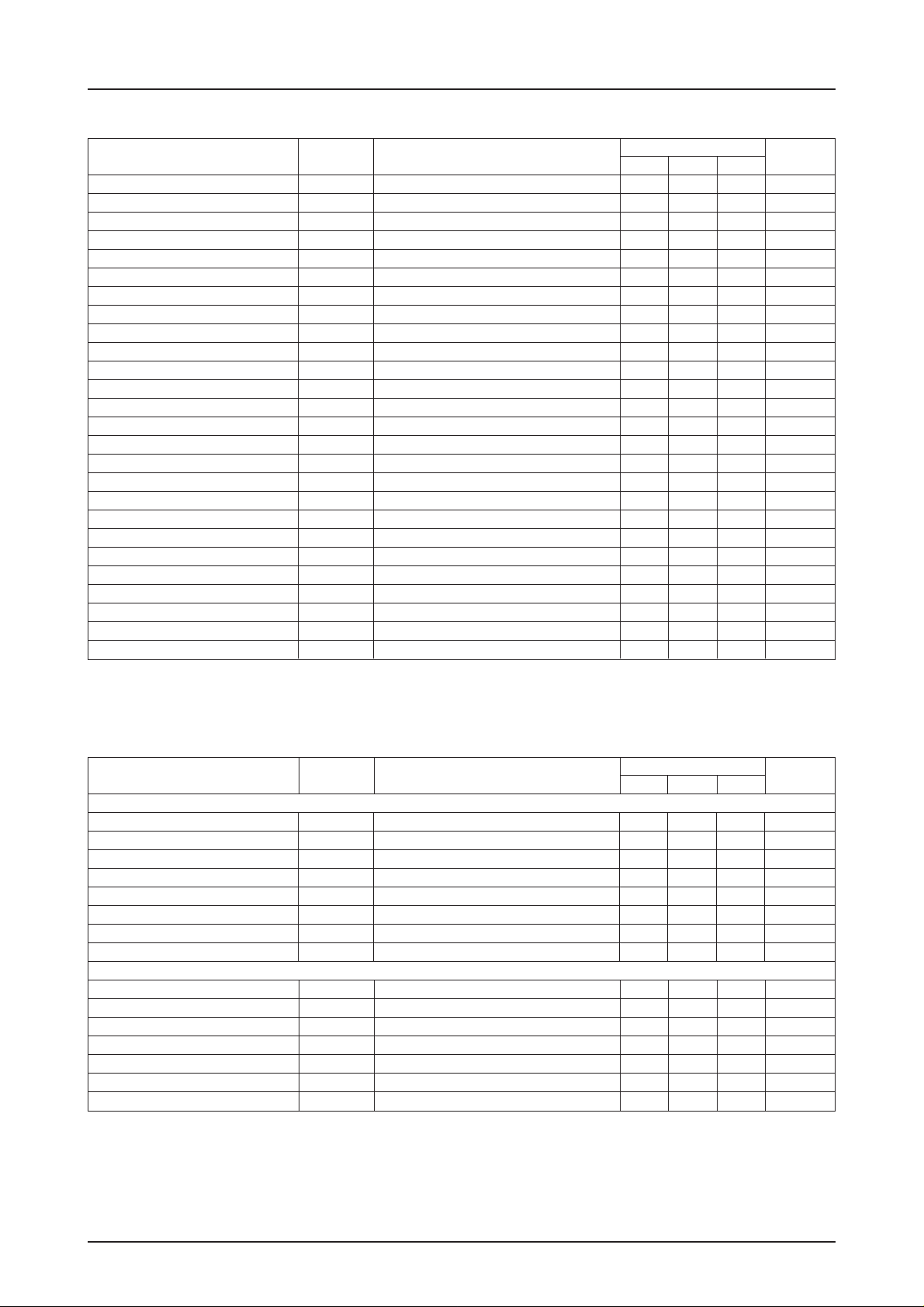
Cylinder Motor Driver Block at Ta = 25°C, VCC1 = 3V, VCC2 = 4.75V, VS = 3V
Parameter Symbol Conditions
Power supply current 4 ICC2 IO = 76 mA VSTBY_D = 3V VSTBY_C = 0V 0.75 2.5 mA
Output idle current 4 ICC2Q VSTBY D = VSTBY_C = 0V 100 µA
Output idle current 5 IS(D)Q VSTBY D = VSTBY_C = 0V 100 300 µA
Output saturation voltage, upper side 1
Output saturation voltage, lower side 1
Output saturation voltage, upper side 2
Output saturation voltage, lower side 2
COM pin common mode input voltage range
Standby pin High level voltage VSTBYH 2 VCC1V
Standby pin Low level voltage VSTBYL –0.2 +0.7 V
Standby pin input current ISTBYH VSTBY_D = 3V 50 µA
Standby pin leakage current ISTBYL VSTBY_D = 0V –10 µA
FRC pin High level voltage VFRCH 2 VCC1V
FRC pin Low level voltage VFRCL –0.2 +0.7 V
FRC pin input current IFRCI VFRC_D = 3V 50 µA
FRC pin leakage current IFRCL VFRC_D = 0V –10 µA
Slope pin source current ratio RSOURCE ICSLP1SOURCE/ICSLP2SOURCE –15 +15 %
Slope pin sink current ratio RSINK ICSLP1SINK/ICSLP2SINK –15 +15 %
CSLP1 source/sink current ratio RCSLP1 ICSLP1SOURCE/ICSLP1SINK –35 +15 %
CSLP2 source/sink current ratio RCSLP2 ICSLP2SOURCE/ICSLP2SINK –35 +15 %
Startup frequency Freq Cosc = 0.1 µF, OSC frequency (Target) 11.5 Hz
Phase delay-width Dwidth (Target) 30 deg
SELCSLP pin High level voltage VSELH 2 VCC1V
SELCSLP pin Low level voltage VSELL –0.2 +0.7 V
SELCSLP pin input current ISELH VSELCSLP = 3V 50 µA
SELCSLP pin leakage current ISELL VSELCSLP = 0V –10 µA
Note) Items shown to be “Target” are not measured.
VOU1 IO = 0.1A RF = 0.25Ω 0.3 0.5 V
VOD1 IO = 0.1A RF = 0.25Ω 0.3 0.5 V
VOU2 IO = 0.4A, VS = 3V RF = 0.25Ω 0.5 0.8 V
VOD2 IO = 0.4A, VS = 3V RF = 0.25Ω 0.5 0.8 V
VIC 0.3
Ratings
min typ max
VCC2–0.9
Unit
V
FG/PG Amplifier Block at Ta = 25°C, VCC1 = 3V, VCC2 = 4.75V, VS = 3V
Parameter Symbol Conditions
[FG amplifier]
Input offset voltage VIO (Target) ±1 ±5mA
Input bias current IBIN– (Target) 250 nA
Common mode input voltage range VICOM (Target) 1 2 V
Open loop gain GVFG f = 1 kHz (Target) 55 dB
Output ON voltage VOL At IO = 10 µA 0.4 V
Output OFF voltage VOH At IO = 10 µA
Schmitt amplifier hysteresis width VSHIS (Target) 50 mV
Reference voltage VREF 1.15 1.30 1.45 V
[PG amplifier]
Input offset voltage VIO (Target) ±1 ±5mV
Input bias current IBIN– (Target) 250 nA
Common mode input voltage range VICOM (Target) 1 2 V
Open loop gain GVPG f = 1 kHz (Target) 55 dB
Output ON voltage VOL At IO = 10 µA 0.4 V
Output OFF voltage VOH At IO = 10 µA
Schmitt amplifier hysteresis width VSHIS (Target) 50 mV
Note) Items shown to be “Target” are not measured.
Ratings
min typ max
VCC1–0.5
VCC1–0.5
Unit
V
V
No. 6216-3/14
Page 4
LB11990W
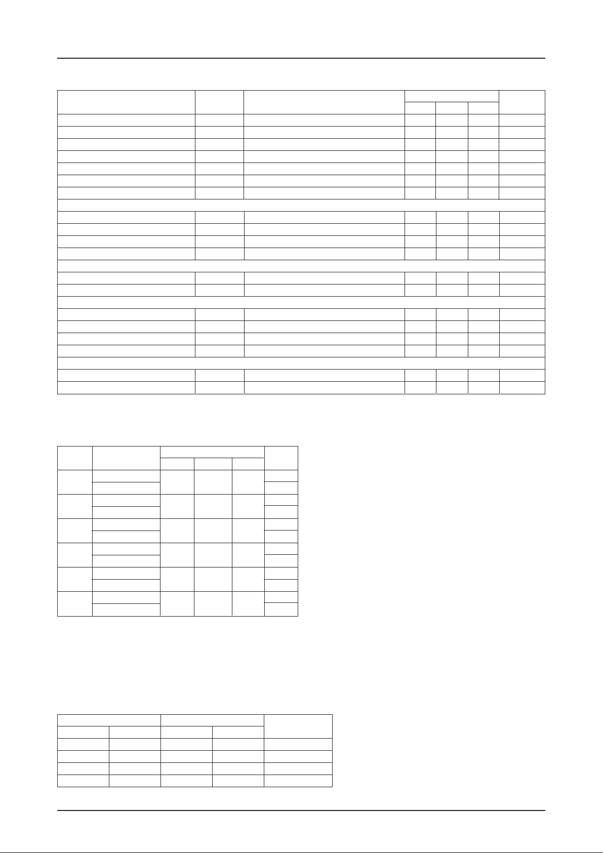
Loading Motor Driver Block at Ta = 25°C, VCC1 = 3V, VCC2 = 4.75V, VS = 3V
Parameter Symbol Conditions
VCC1 power supply current 1 ICC11 VSTBY_C = VSTBY_D = 0V (standby) 2.1 4 mA
VCC1 power supply current 2 ICC12
VCC1 power supply current 3 ICC13 VSTBY_C = VSTBY_D = 0V (at braking) 10 14 mA
VCC2 power supply current 1 ICC21
VCC2 power supply current 2 ICC22 VSTBY_C, D = 0V (standby (VCC1 = 3.0V)) 100 µA
VCC2 power supply current 3 ICC23 VSTBY_C, D = 0V (forward/reverse) 15.0 25 mA
VS L power supply current I VS L VSTBY_C, D = 0V (standby) 20 µA
[Logic input (DEC1 pin, DEC2 pin)]
High level input voltage VINH VCC1 = 2.7 to 4.0V 2.0 VCC1V
High level flowing current IINH VIN = 3.0V 41 65 µA
Low level input voltage VINL VCC1 = 2.7 to 4.0V –0.2 0.6 V
Low level flowing current IINL VIN = 0.6V 5 10 µA
[Loading motor driver]
Output saturation voltage 1 VOH IO = 200 mA (upper/lower composition) 0.2 0.3 V
Output saturation voltage 2 VSHIS IO = 400 mA (upper/lower composition) 0.4 0.6 V
[Reel FG amplifier]
Input offset voltage VIO ±1 ±5mV
Input bias current IB 1 µA
Common mode input voltage range VICM 1 2 V
Open loop gain GV1 55 dB
[Thermal shutdown circuit]
TSD operating temperature T-TSD (Target) 180 °C
TSD temperature hysteresis width ∆TSD (Target) 15 °C
Note) Items shown to be “Target” are not measured.
VSTBY_C = VSTBY_D = 0V (forward/reverse)
VSTBY_C, D = 0V (standby (VCC1 = OPEN))
Ratings
min typ max
14 19 mA
Unit
100 µA
Truth Table
Capstan Motor Truth Table
Hall input
Source –> Sink U V W FRC
1
2
3
4
5
6
Note: “H” for FR means a voltage of 2.50V or above. “L” for FR means a voltage of 0.4V or below.
Note: At the Hall input, “H” means that the potential of the (+) terminal for each phase input is at least 0.02V higher than the (–) terminal.
V –> W
W –> V L
U –> W
W –> U L
U –> V
V –> U L
W –> V
V –> W L
W –> U
U –> W L
V –> U
U –> V L
(Vcc1 = 3V)
“L” means that the potential of the (+) terminal for each phase input is at least 0.02V lower than the (–) terminal.
HHL
HLL
HLH
LLH
LHH
LHL
Loading Motor Truth Table
Input Output Mode
DEC1 DEC2 OUT1 OUT2
L L Off Off Standby
H L H L Forward
L H L H Reverse
H H L L Brake
H
H
H
H
H
H
No. 6216-4/14
Page 5
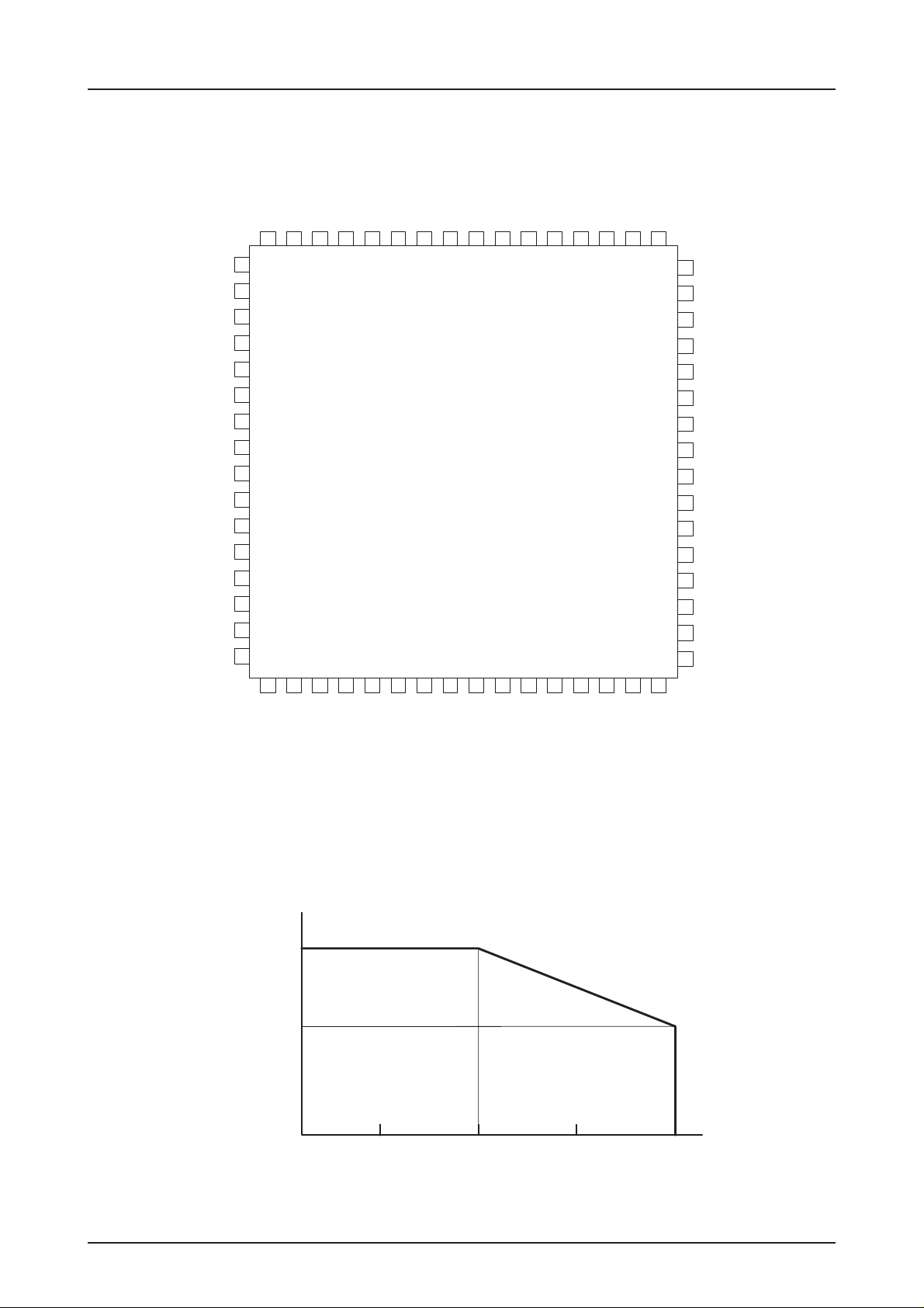
Pin Assignment
UIN2
UIN1
WOUT_C
RF_C
VOUT_C
NC
UOUT_C
WOUT_D
RF_D
VOUT_D
UOUT_D
VS_D
OUT2
RF_L
OUT1
RS_L
585960616264 63 4950515253545557 56
VIN1
48
1
VIN2
47
2
WIN1
46
3
WIN2
45
4
LB11990W
VS_C
VH+
VH–
42
43
44
LB11990W
7
6
5
VCC2
41
8
FRC_C
39
40
9
ANGLE
FGIN+
38
11
10
FGIN–
37
12
FGOUT_C
FGOUT_D
35
36
14
13
FGIN1_D
FGIN2_D
33
34
16
15
FGIN_D
VREF
PGIN
PGC
PGOUT_D
GND
WIN
VIN
UIN
COM
232221201917 18 3231302928272624 25
VCC1
FC2
FILTER
FC1
OSC
FRC_D
NC
0.6
0.36
Power dissipation, Pd max [W]
0
DEC2
RLM1
VS_L
Ambient temperature, Ta [°C]
DEC1
STBY_C
RLP1
RLO1
RLO2
Pd max – Ta
RLP2
RLM2
CSLP1
SELCSLP
BFGO
CSLP2
STBY_D
Top view
75–20 25 500
No. 6216-5/14
Page 6
LB11990W
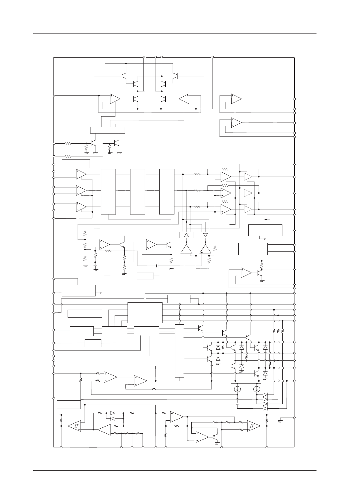
Block Diagram
RS_L
DEC1
DEC2
NC
Forward/reverse
switching
1.2V reference
voltage bias start
circuit
Reference
voltage
VCC1
30k
FRC_C
UIN1
UIN2
VIN1
VIN2
WIN1
WIN2
ANGLE
VCC1
STBY_D
BFGO
FC2
OSC
FRC_D
CSLP1
CSLP2
SELCSLP
FC1
FILTER
2×R1
R1
R1
TSD circuit
Startup
control circuit
Forward/
reverse
30k
VCC2
DECORDER
R2
VX
200
200
40k
Hall input synthesis
(matrix)
VCC2
R2
R4
R3
Cylinder bias circuits
Timing control
circuit
10k
200
9k 1k200
OUT1 OUT2 VS_L RF_L
R5
R5
Matrix signal level shift
VX+α
+Vf
Rotor
position
detector
Soft switching
drive circuit
200
500
Drive signal current
generator
1.5×R5
Mid point
control
100k
500
R5
VX+Vf
Output drive circuit
R5
R5
R5
TSD
Upper/lower
amplitude limiter
SBDSBD
VS–VX–Vf+2α
R6
(VS/2)+α
R6
B
B
B
1.2V reference
voltage bias start
circuit
Hall power
supply voltage
output circuit
20075k1.5k
200
VCC1
Capstan bias
circuits
VCC1
VCC1
VCC1
30k
RLO1
RLM1
RLP1
RLO2
RLM2
RLP2
VS_C
UOUT_C
VOUT_C
WOUT_C
RF_C
STBY_C
VH+
VH–
FGOUT_C
FGIN–
FGIN+
VCC2
COM
WIN
VIN
UIN
VS_D
UOUT_D
VOUT_D
WOUT_D
RF_D
GND
FGIN2_D
FGIN1_D
FGIN_D VREFFGOUT_D
PGIN
PGOUT_DPGC
Unit (resistance: Ω)
No. 6216-6/14
Page 7
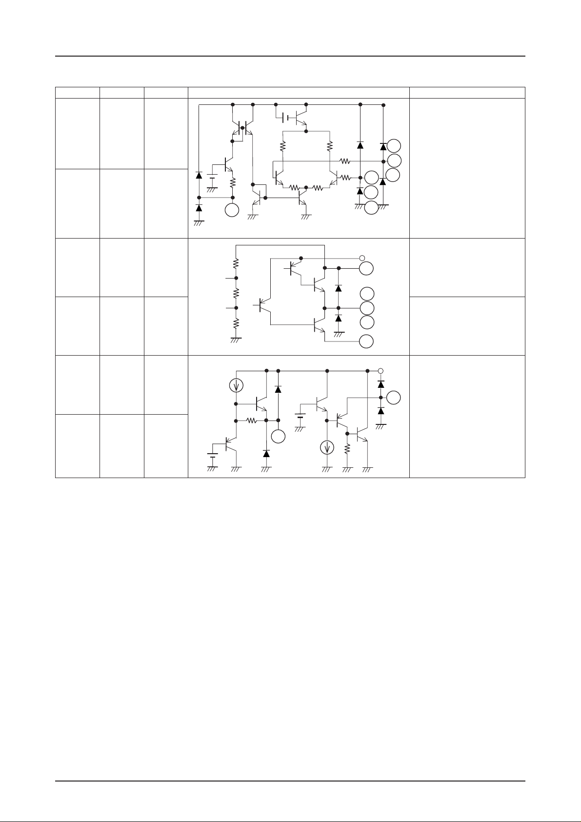
Pin Description
Pin number
50
49
48
47
46
45
39
Pin name
Uin1
Uin2
Vin1
Vin2
Win1
Win2
ANGLE
Pin voltage
0 to VCC1
TYP
1.2V
39
LB11990W
Equivalent circuit
0.3V
4kΩ
Ω
200
400Ω
400Ω
Pin function
Capstan motor driver U, V, W
phase Hall element input/output
pins. Logic High means IN1 > IN2.
4kΩ
200Ω
46
48
50
45
200Ω
47
49
44
55
53
51
52
43
42
VS_C
U-OUT_C
V-OUT_C
W-OUT_C
RF_C
VH+
VH–
0 to VCC2
1/4*Vs
1/4*Vs
approx.
1.9V
10kΩ
5kΩ
5kΩ
20kΩ
43
0.9V
Capstan motor output amplitude
VCC2
44
control power supply pins.
Voltage must be lower than
VCC2.
51
53
Capstan motor driver U, V, W
phase output pins.
55
52
Hall element bias voltage supply
VCC1
pins. A voltage of 0.85V (typ.) is
generated between VH+ and
VH– (at IH = 5 mA).
42
20kΩ
Continued on next page
No. 6216-7/14
Page 8
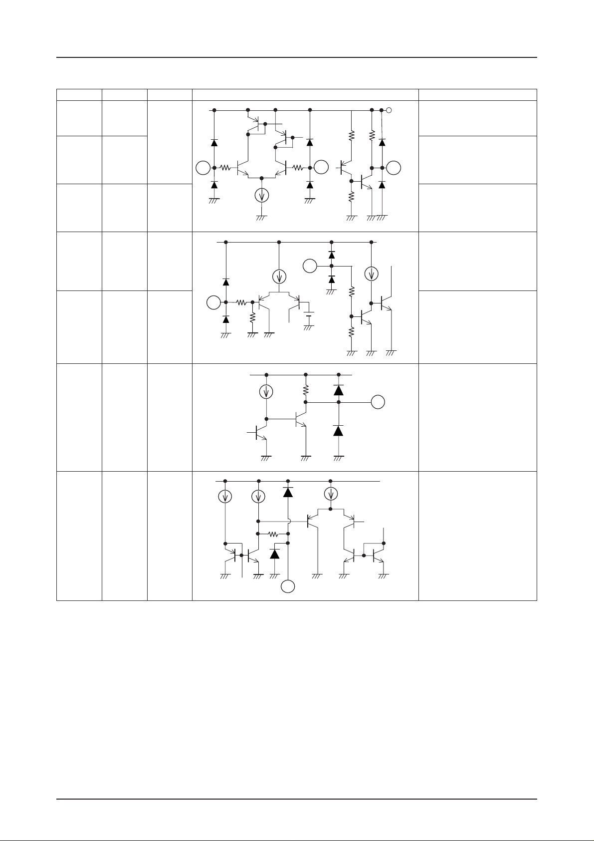
Continued from preceding page
Pin number
37
Pin name
FGIN–
Pin voltage
0 to VCC1
LB11990W
Equivalent circuit Pin function
FG comparator inverted input pin.
VCC1
No internal bias is applied.
38
36
40
35
2
FGIN+
FGOUT_C
FRC_C
STBY_C
FGOUT_D
0 to VCC1
37
40
200Ω
VCC1
20kΩ
15kΩ
200Ω
38
50kΩ
36
VCC1
2
100kΩ
100kΩ
30µA
30kΩ
35
FG comparator non-inverted
input pin. No internal bias is
applied.
FG comparator output pin.
Internal load impedance is 20 kΩ.
Capstan motor forward/reverse
select pin. The voltage at this pin
(with hysteresis) selects forward
or reverse rotation.
This pin selects bias supply to
capstan circuits other than FG
comparator. Setting the pin to
Low cuts off the bias supply.
Capstan motor standby pin.
FG amplifier output pin.
18
OSC
V
CC
5µA
2.5µA
1kΩ
10µA
Pin for connecting triangular
1
wave oscillator capacitor. Serves
for forced startup waveform
generation.
18
Continued on next page
No. 6216-8/14
Page 9
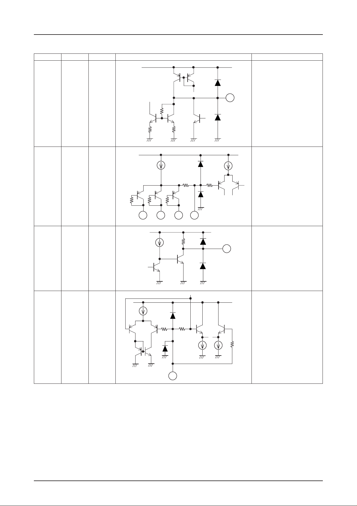
Continued from preceding page
Pin number
19
Pin name
FC1
Pin voltage
VCC1
LB11990W
Equivalent circuit Pin function
Frequency characteristics pin.
Connecting a capacitor between
this pin and ground serves to
prevent closed-loop oscillation in
the current control circuitry.
19
2kΩ
20
28
29
FILTER
PGOUT D
PGC
VCC1
1kΩ
VCC1
5kΩ
1kΩ
10kΩ
Connecting a capacitor between
this pin and ground activates the
25µA
30kΩ
1kΩ
1kΩ
coil output saturation prevention
function. In this condition, the VS
pin is controlled for motor voltage
control.
By adjusting the external capacitor,
torque ripple compensation can be
varied.
20595856
PG amplifier output pin.
30µA
30kΩ
28
VCC1
PG amplifier peak hold capacitor
connection pin.
6µA
1.5kΩ
29
75kΩ
10µA
10µA
200Ω
Continued on next page
No. 6216-9/14
Page 10
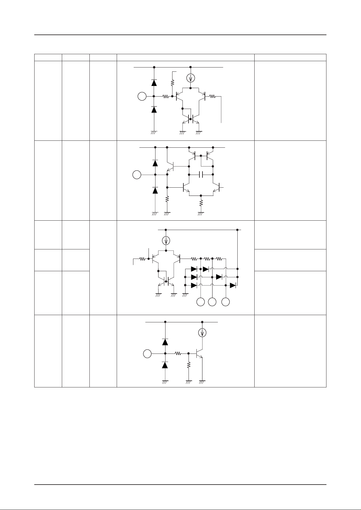
Continued from preceding page
Pin number
30
Pin name
PGIN
Pin voltage
max2.0V
min1.0V
(At VCC =
3V)
30
LB11990W
Equivalent circuit Pin function
PG amplifier input pin.
Connect PG coil between this pin
and VREF.
500Ω
VCC1
6µA
100kΩ
500Ω
1.3V
31
32
33
34
16
VREF
FGIN_D
FGIN1_D
FGIN2_D
STBY_D
max2.0V
min1.0V
(At VCC1 =
3V)
0 to VCC1
31
500Ω
1.3V
V
16
CC
VCC1
1.3V
35kΩ
1
6µA
100kΩ
34
70kΩ
33 32
VCC1
Internal 1.3V reference voltage.
Used as reference voltage for FG
and PG amplifiers.
FG amplifier input pin.
Connect FG coil between this pin
and VREF.
FG amplifier input signal noise
filter capacitor connection.
FG amplifier input signal noise
filter capacitor connection.
When this pin is at 0.7V or lower
or when it is open, only the FG/
PG amplifier operates.
In the motor drive state, the pin
should be at 2V or higher.
Drum motor standby pin.
100kΩ
Continued on next page
No. 6216-10/14
Page 11
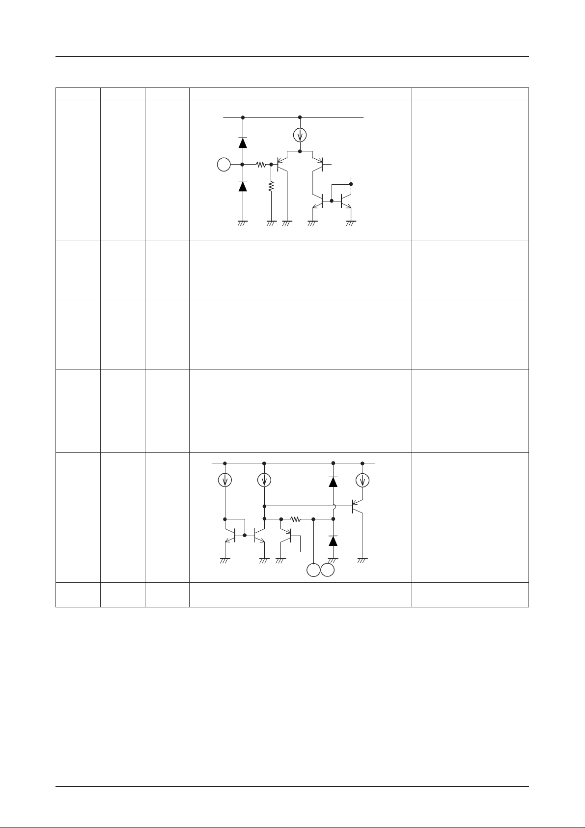
Continued from preceding page
Pin number
17
Pin name
FRC_D
Pin voltage
0 to VCC1
17
LB11990W
Equivalent circuit Pin function
Drum motor forward/reverse
VCC1
20µA
50kΩ
50kΩ
rotation select pin.
Low: forward
(–0.2V to 0.7V or open)
High: reverse
(2V to VCC1)
60
41
22
13
14
VS_D
VCC2
VCC1
CSLP1
CSLP2
0V to VCC2
3.5V to 8.5V
2.7V to 6V
Power supply pin for determining
output amplitude by supplying
drum motor voltage.
Must be lower than VCC2 voltage.
Power supply pin for supplying
source side predriver voltage and
coil waveform detect comparator
voltage. Common for loading,
capstan, and drum motors.
Power supply pin for circuits
except motor voltage, source
side predriver voltage, and coil
waveform detect comparator
voltage.
Common for loading, capstan,
and drum motors.
Pins for connecting triangular
VCC1
10µA
5µA
1kΩ
5µA
wave oscillator capacitor. This
triangular wave coil output
performs waveform soft switching.
27
GND
13
14
Ground pin for all circuits except
output.
Continued on next page
No. 6216-11/14
Page 12
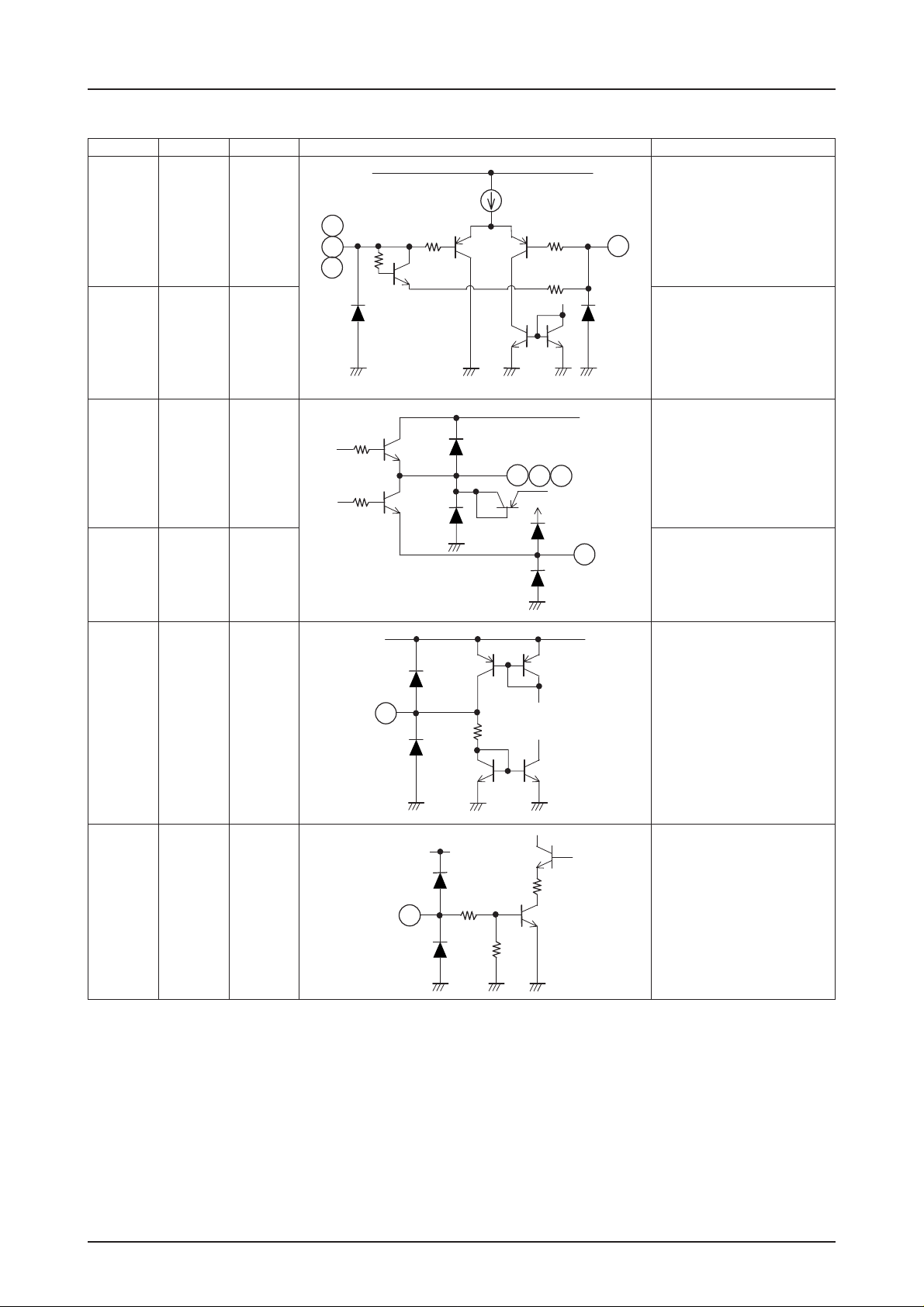
Continued from preceding page
Pin number
26
24
25
23
Pin name
WIN
UIN
VIN
COM
Pin voltage
26
25
24
VCC1
LB11990W
2kΩ
Equivalent circuit Pin function
Coil waveform detect comparator
input pins.
10µA
200Ω
200Ω
200Ω
23
Motor coil midpoint input pin.
Using this voltage as a reference,
the coil voltage waveform is
detected.
56
59
58
57
21
12
WOUT_D
UOUT_D
VOUT_D
RF_D
FC2
SELCSLP
0 to VCC1
3.9Ω
3.9Ω
VCC1
21
VCC1
12
100kΩ
VS_D
56
58 59
VCC1
57
10kΩ
10kΩ
U, V, W phase coil output pins.
Drum motor driver output
transistor ground. Constant
current drive is performed by
detecting the voltage at this pin.
Output midpoint control.
Oscillation prevention capacitor
connection pin.
When High, this pin sets CSLP
slant to 15 times the slant at Low.
When VCC1 = 3.0V
2.0V or higher: High
0.7V or lower: Low
100kΩ
Continued on next page
No. 6216-12/14
Page 13
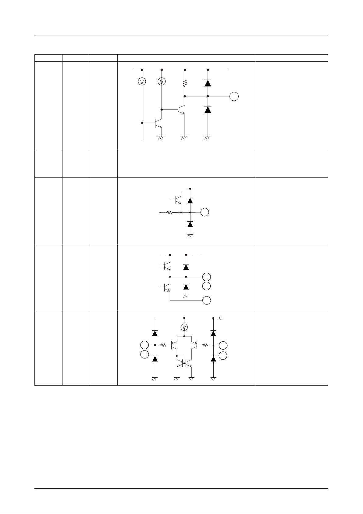
Continued from preceding page
Pin number
15
Pin name
BFGO
Pin voltage
LB11990W
Equivalent circuit Pin function
VCC1
5µA
50µA
30kΩ
15
Motor counter EMF voltage FG
pulse pin.
Outputs a pulse using W phase
counter EMF voltage as FG.
Connect to ground if not used.
62
63
61
11
10
5
VS_L
RF_L
OUT1
OUT2
2.2 to VCC2
1kΩ
VS_L
62
VS_L
Loading motor power supply pin.
Stabilize against noise in the
same way as for VCC2.
Output transistor P–GND
Output current can be detected
for motor current control by
inserting a resistor between Rf
pin and ground.
Loading motor driver output pins.
Connect to loading motor.
61
63
62
6
7
RLM1
RLP1
RLM2
RLP2
0 to VCC1
10kΩ 10kΩ
6
11
VCC1
7
10
L–FG amplifier input pins.
RLM1 and RLM2 are negative
input.
RLP1 and RLP2 are positive
input.
Continued on next page
No. 6216-13/14
Page 14
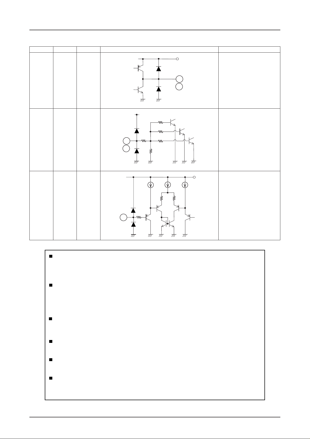
Continued from preceding page
Pin number
8
9
Pin name
RLO1
RLO2
Pin voltage
LB11990W
Equivalent circuit Pin function
VCC1
8
9
R–FG amplifier output pins.
3
4
DEC1
DEC2
0 to VCC1
V
CC
50kΩ
1
10kΩ
10kΩ
10kΩ
Loading motor input pins.
When VCC1 = 3.0V
2.0V or higher: High
0.6V or lower: Low
3
64
RS_L
4
0 to VCC1
–1.5V
1kΩ
75Ω
Current limiter setting pin.
VCC1
Set voltage between RF pin and
ground, for limiting current.
64
Specifications of any and all SANYO products described or contained herein stipulate the performance,
characteristics, and functions of the described products in the independent state, and are not guarantees
of the performance, characteristics, and functions of the described products as mounted in the customer's
products or equipment. To verify symptoms and states that cannot be evaluated in an independent device,
the customer should always evaluate and test devices mounted in the customer's products or equipment.
SANYO Electric Co., Ltd. strives to supply high-quality high-reliability products. However, any and all
semiconductor products fail with some probability. It is possible that these probabilistic failures could
give rise to accidents or events that could endanger human lives, that could give rise to smoke or fire,
or that could cause damage to other property. When designing equipment, adopt safety measures so
that these kinds of accidents or events cannot occur. Such measures include but are not limited to protective
circuits and error prevention circuits for safe design, redundant design, and structural design.
In the event that any or all SANYO products(including technical data,services) described or
contained herein are controlled under any of applicable local export control laws and regulations,
such products must not be exported without obtaining the export license from the authorities
concerned in accordance with the above law.
No part of this publication may be reproduced or transmitted in any form or by any means, electronic or
mechanical, including photocopying and recording, or any information storage or retrieval system,
or otherwise, without the prior written permission of SANYO Electric Co. , Ltd.
Any and all information described or contained herein are subject to change without notice due to
product/technology improvement, etc. When designing equipment, refer to the "Delivery Specification"
for the SANYO product that you intend to use.
Information (including circuit diagrams and circuit parameters) herein is for example only ; it is not
guaranteed for volume production. SANYO believes information herein is accurate and reliable, but
no guarantees are made or implied regarding its use or any infringements of intellectual property rights
or other rights of third parties.
This catalog provides information as of November, 1999. Specifications and information herein are subject to change
without notice.
No. 6216-14/14
PS
 Loading...