

Page 1
Monolithic Linear IC
61202RM (OT) No. 7104-1/17
SANYO Electric Co.,Ltd. Semiconductor Company
TOKYO OFFICE Tokyo Bldg., 1-10, 1 Chome, Ueno, Taito-ku, TOKYO, 110-8534 JAPAN
Direct PWM Drive Brushless Pre-Driver for
Household Appliance Motors
LB11820M
Ordering number : ENN7104A
Parameter Symbol Conditions Ratings Unit
Maximum supply voltage 1 V
CC
1 max VCC1 14.5 V
Maximum supply voltage 2 V
CC
2 max VCC2 14.5 V
Maximum supply voltage 3 V
CC
3 max VCC320V
Specifications
Absolute Maximum Ratings at Ta = 25°C
Any and all SANYO products described or contained herein do not have specifications that can handle
applications that require extremely high levels of reliability, such as life-support systems, aircraft’s
control systems, or other applications whose failure can be reasonably expected to result in serious
physical and/or material damage. Consult with your SANYO representative nearest you before using
any SANYO products described or contained herein in such applications.
SANYO assumes no responsibility for equipment failures that result from using products at values that
exceed, even momentarily, rated values (such as maximum ratings, operating condition ranges, or other
parameters) listed in products specifications of any and all SANYO products described or contained
herein.
Overview
The LB11820M is a direct PWM drive pre-driver IC that
is appropriate for 3-phase power brushless motors. This IC
can implement motor driver circuits that provide the
desired output capabilities (voltage and current) by the use
of appropriate discrete transistors in the output circuit. The
LB11820M is optimal for driving the large motors used in
air conditioners and on-demand hot water heaters.
Functions and Features
• Three-phase bipolar drive
• Direct PWM drive
• Built-in braking function (Short braking)
• Forward/reverse switching function
• Reverse motion mode protection circuit
• Full complement of protection circuits, include current
limiter, low-voltage protection, and motor constraint
(rotor locking) protection circuits
• Supports control from either a command voltage or a
PWM duty input.
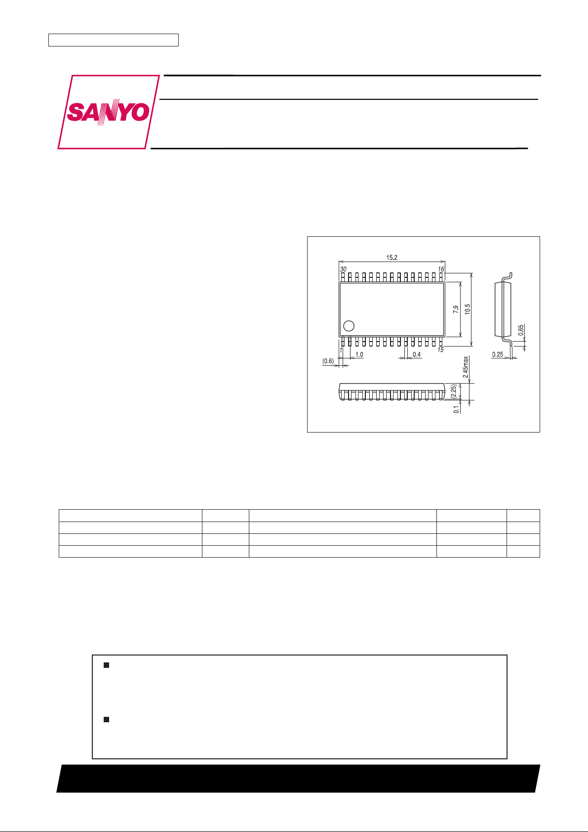
Package Dimensions
unit: mm
3073C-MFP30SD (375mil)
SANYO: MFP30SD(375mil)
[LB11820M]
Continued on next page.
Page 2
No. 7104-2/17
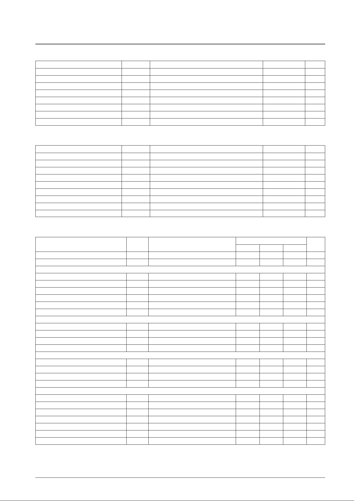
LB11820M
Parameter Symbol Conditions
Ratings
Unit
min typ max
Supply current 1 ICC1-1 15 20 mA
Supply current 2 I
CC
1-2 When stopped 2.5 4 mA
[Output Block]
Output voltage 1-1 V
OUT
1-1 Low level, IO= 400 µA 0.1 0.3 V
Output voltage 1-2 V
OUT
1-2 Low level, IO= 10 mA 0.8 1.1 V
Output voltage 2 V
OUT
2 High level, IO= –20 mA
VCC1 – 1.1 VCC1 – 0.9
V
Temperature coefficient 1-1 ∆V
OUT
1-1 Design target value*, low level, IO= 400 µA 0.2 mV / °C
Temperature coefficient 1-2 ∆V
OUT
1-2 Design target value*, low level, IO = 10 mA –1.5 mV / °C
Temperature coefficient 2 ∆V
OUT
2 Design target value*, high level, IO= –20 mA 1.5 mV / °C
[12 V Voltage Output (12REG pin)]
Output voltage V12REG V
CC
3 = 15 V, IO= –30 mA 11.7 12.1 12.6 V
Line regulation
∆V12REG1
VCC3 = 13.5 to 19 V, IO= –30 mA 150 300 mV
Load regulation
∆V12REG2
IO= –5 to –45 mA, VCC3 = 15 V 100 200 mV
Temperature coefficient
∆V12REG3
Design target value* 2 mV / °C
[5 V Voltage Output (VREG pin)]
Output voltage VREG 4.7 5.0 5.3 V
Line regulation
∆VREG1
VCC1 = 8 to 13.5 V 40 100 mV
Load regulation
∆VREG2
IO= –5 to –20 mA 5 30 mV
Temperature coefficient
∆VREG3
Design target value* 0 mV / °C
[Hall Amplifier Block]
Input bias current
IHB(HA)
–2 –0.5 µA
Common-mode input voltage range 1
VICM1
When Hall effect devices are used 0.5
VCC1 – 2.0
V
Common-mode input voltage range 2
VICM2
When single-sided input bias is used (Hall IC application)
0 VCC1 V
Hall input sensitivity 50 mVp-p
Hysteresis
∆VIN(HA)
20 30 50 mV
Input voltage low––>high
VSLH(HA)
5 15 25 mV
Input voltage high––>low
VSHL(HA)
–25 –15 –5 mV
Parameter Symbol Conditions Ratings Unit
Maximum output current I
O
max The UL, VL, WL, UH, VH, and WH pins 40 mA
Maximum RF pin applied voltage VRF max 4 V
Maximum LVS pin applied voltage VLVS max 20 V
Maximum TOC pin applied voltage VTOC max V
CC
2 V
Maximum VCTL pin applied voltage VCTL max 14.5 V
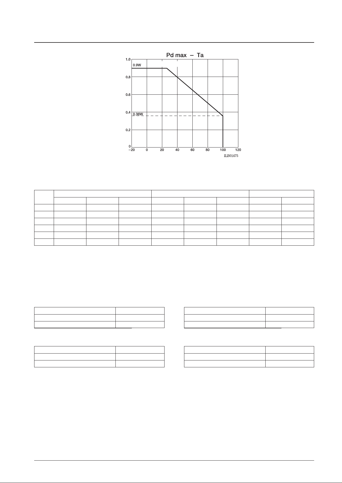
Allowable power dissipation Pd max Independent IC 0.9 W
Operating temperature Topr –20 to +100 °C
Storage temperature Tstg –55 to +150 °C
Parameter Symbol Conditions Ratings Unit
Supply voltage range 1-1 V
CC
1-1 VCC1 8 to 13.5 V
Supply voltage range 1-2 V
CC
1-2 VCC1, with VCC1 and VREG shorted together 4.5 to 5.5 V
Supply voltage range 2 V
CC
2 VCC2 4.5 to VCC1 V
Supply voltage range 3 V
CC
3 VCC3 13.5 to 19 V
Output current I
O
The UL, VL, WL, UH, VH, and WH pins 30 mA
12 V regulator voltage output current I12REG –50 mA
5 V regulator voltage output current IREG –20 mA
HP pin applied voltage VHP 0 to 13.5 V
HP pin output current IHP 0 to 10 mA
Allowable Operating Ranges at Ta = 25°C
Electrical Characteristics at Ta = 25°C, VCC1 = 12 V, VCC2 = V
REG
* : These are design target values and are not tested.
Continued on next page.
Continued from preceding page.
Continued on next page.
Page 3
No. 7104-3/17
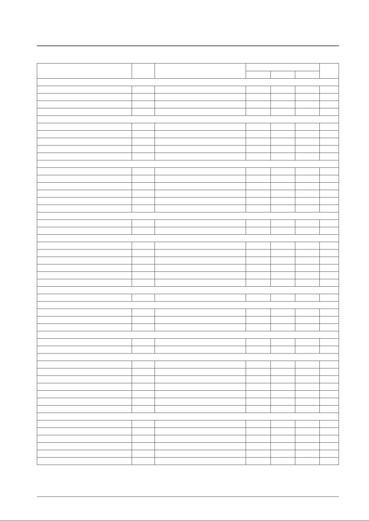
LB11820M
Parameter Symbol Conditions
Ratings
Unit
min typ max
[VCTL Pin]
Input voltage 1 VCTL1 Output duty : 0% 1.05 1.4 1.75 V
Input voltage 2 VCTL2 Output duty : 100% 3.0 3.5 4.1 V
Input bias current 1 IB1(CTL) VCTL = 0 V –80 –60 µA
Input bias current 2 IB2(CTL) VCTL = 5 V 60 80 µA
[PWM Oscillator (PWM pin)]
High-level output voltage
VOH(PWM)
2.75 3.0 3.25 V
Low-level output voltage
VOL(PWM)
1.0 1.2 1.3 V
External capacitor charge current ICHG VPWM = 2.1 V –60 –45 –30 µA
Oscillator frequency f(PWM) C = 1000pF 17.6 22 26.8 kHz
Amplitude V(PWM) 1.6 1.8 2.1 Vp-p
[TOC pin]
Input voltage 1 VTOC1 Output duty : 0% 2.72 3.0 3.30 V
Input voltage 2 VTOC2 Output duty : 100% 0.99 1.2 1.34 V
Input voltage 1L VTOC1L
Design target value*, when VCC2 = 4.7 V, 0%
2.72 2.80 2.90 V
Input voltage 2L VTOC2L
Design target value*, when VCC2 = 4.7 V, 100%
0.99 1.08 1.17 V
Input voltage 1H VTOC1H
Design target value*, when VCC2 = 5.3 V, 0%
3.08 3.20 3.30 V
Input voltage 2H VTOC2H
Design target value*, when VCC2 = 5.3 V, 100%
1.11 1.22 1.34 V
[HP pin]
Output saturated voltage VHPL I
O
= 7 mA 0.15 0.5 V
Output leakage current IHP leak V
O
= 13.5 V 10 µA
[CSD Oscillator (CSD pin)]
High-level output voltage
VOH(CSD)
3.2 3.6 4.0 V
Low-level output voltage
VOL(CSD)
0.9 1.1 1.3 V
External capacitor charge current ICHG1 –14 –10 –6 µA
External capacitor discharge current ICHG2 7 11 15 µA
Oscillator frequency f(CSD) C = 0.01 µF 200 Hz
Amplitude V(CSD) 2.2 2.5 2.75 Vp-p
[Current Limiter Circuit (RF pin)]
Limiter voltage VRF 0.45 0.5 0.55 V
[Low-Voltage Protection Circuit (LVS pin)]
Operating voltage VSDL 3.6 3.8 4.0 V
Release voltage VSDH 4.1 4.3 4.5 V
Hysteresis ∆VSD 0.35 0.5 0.65 V
[Thermal Shutdown Circuit (Thermal protection circuit)]
Thermal shutdown temperature TSD Design target value* (Junction temperature) 125 145 165 ˚C
Hysteresis ∆TSD Design target value* (Junction temperature) 20 25 30 ˚C
[PWMIN Pin]
Input frequency f(PI) 50 kHz
High-level input voltage V
IH
(PI) 2.0 VREG V
Low-level input voltage V
IL
(PI) 0 1.0 V
Input open voltage V
IO
(PI)
VREG – 0.5
VREG V
Hysteresis V
IS
(PI) 0.2 0.3 0.4 V
High-level input current I
IH
(PI) VPWMIN = VREG –10 0 10 µA
Low-level input current I
IL
(PI) VPWMIN = 0 V –130 –96 µA
[S/S Pin]
High-level input voltage V
IH
(SS) 2.0 VREG V
Low-level input voltage V
IL
(SS) 0 1.0 V
Input open voltage V
IO
(SS)
VREG – 0.5
VREG V
Hysteresis V
IS
(SS) 0.2 0.3 0.4 V
High-level input current I
IH
(SS) VS/S = VREG –10 0 10 µA
Low-level input current I
IL
(SS) VS/S = 0 V –130 –96 µA
* : These are design target values and are not tested.
Continued from preceding page.Continued from preceding page.
Continued on next page.
Page 4

No. 7104-4/17
LB11820M
Parameter Symbol Conditions
Ratings
Unit
min typ max
[F/R Pin]
High-level input voltage V
IH
(FR) 2.0 VREG V
Low-level input voltage V
IL
(FR) 0 1.0 V
Input open voltage V
IO
(FR)
VREG – 0.5
VREG V
Hysteresis V
IS
(FR) 0.2 0.3 0.4 V
High-level input current I
IH
(FR) VF/R = VREG –10 0 10 µA
Low-level input current I
IL
(FR) VF/R = 0 V –130 –96 µA
[BR Pin]
High-level input voltage V
IH
(BR) 2.0 VREG V
Low-level input voltage V
IL
(BR) 0 1.0 V
Input open voltage V
IO
(BR)
VREG – 0.5
VREG V
Hysteresis V
IS
(BR) 0.2 0.3 0.4 V
High-level input current I
IH
(BR) VBR = VREG –10 0 10 µA
Low-level input current I
IL
(BR) VBR = 0 V –130 –96 µA
[REVSEL Pin]
High-level input voltage
VIH(RSEL)
2.0 VREG V
Low-level input voltage
VIL(RSEL)
0 1.0 V
Input open voltage
VIO(RSEL)
VREG – 0.5
VREG V
High-level input current
IIH(RSEL)
VREVSEL = VREG –10 0 10 µA
Low-level input current
IIL(RSEL)
VREVSEL = 0 V –130 –96 µA
Continued from preceding page.
Page 5
No. 7104-5/17
LB11820M
Ambient temperature, Ta — °C
Allowable power dissipation, Pdmax — W
When the OFF mode is selected during reversing at the REVSEL pin, it is necessary to specify the Hall input condition.
With F/R = "L", the condition in which the Hall input is entered in the order from 1 to 6 in the above table is considered the forward rotation and that in the
reverse order is considered reversing.
With F/R = "H", the condition in which the Hall input is entered in the order from 6 to 1 in the above table is considered the forward rotation and that in the
reverse order is considered reversing.
When S/S and PWMIN pins are not used, set the input to the L level voltage.
When REVSEL and BR pins are not used, set the input to the H level voltage or the open condition.
F / R = (L) F / R = (H) Output
IN1 IN2 IN3 IN1 IN2 IN3 PWM –
1 H L H L H L VH UL
2 H L L L H H WH UL
3 H H L L L H WH VL
4 L H L H L H UH VL
5 L H H H L L UH WL
6 L L H H H L VH WL
Three-Phase Logic Truth Table (IN = "H" refers to the state where IN+> IN–.)
S/S Pin
Independent IC
Input state State
High or open Stop
Low Start
REVSEL Pin
Input state State
High or open –
Low Off in reverse
BR Pin
Input state State
High or open –
Low Brake
PWIM Pin
Input state State
High or open Output off
Low Output on
Page 6
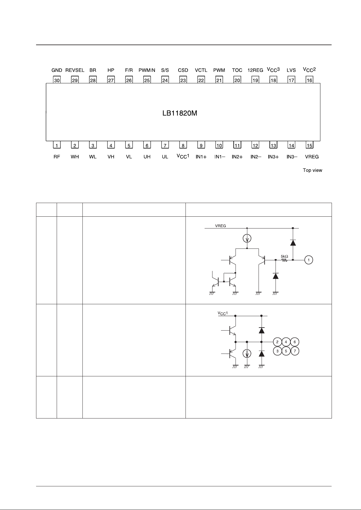
Pin Assignment
No. 7104-6/17
LB11820M
Pin No.
1
2
4
6
3
5
7
8
Pin
RF
WH
VH
UH
WL
VL
UL
V
CC
1
Equivalent circuitFunction
Output current detection
Connect a resistor (Rf) between this pin and ground.
Set with the maximum output current I
OUT
= 0.5/Rf.
Output pin (external TR drive output)
Duty control made on UH, VH, and WH sides.
Power supply (output and Hall input blocks).
Normally used with the 12 V power supply. Connect
to V
CC
2 and VREG for application with the 5 V single
power supply. Connect a capacitor between this pin
and GND for stabilization.
Continued on next page.
Page 7
No. 7104-7/17
LB11820M
Pin No.
9
10
11
12
13
14
15
16
17
18
19
20
Pin
IN1+
IN1–
IN2+
IN2–
IN3+
IN3–
VREG
V
CC
2
LVS
V
CC
3
12REG
TOC
Equivalent circuitFunction
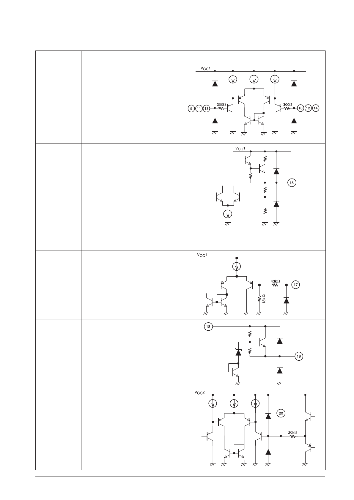
Hall amplifier input.
IN+ > IN– is the input high state, and the reverse is
the input low state.
Connect a capacitor between the sIN+ and IN–
inputs if there is noise in the Hall sensor signals.
Regulated-voltage output pin (5V output)
Connect a capacitor (about 0.1 µF) between this pin
and ground for stabilization.
Voltage detection pin for low-voltage protection.
To detect the supply voltage of 5 V or more, connect
the zenor diode in series to set the detection voltage.
Power pin (V
CC
3) for use during application with the
supply voltage of 12 V or more. 12 V is generated at
the 12 REG pin. To use the 12REG pin, connect this
pin to V
CC
1.
When not used, keep both V
CC
3 and 12 REG open
or connect them to GND.
PWM waveform comparator pin.
Normally used in the open condition.
By inputting the voltage directly into this pin, the
output duty can be controlled without using the
VCTL amp.
Power pin (PWM oscillation, PWM comparator,
VCTL amp). Normally connect to VREG.
Continued on next page.
Continued from preceding page.
Page 8
No. 7104-8/17
LB11820M
Pin No.
21
22
23
24
25
Pin
PWM
VCTL
CSD
S / S
PWM
IN
Equivalent circuitFunction
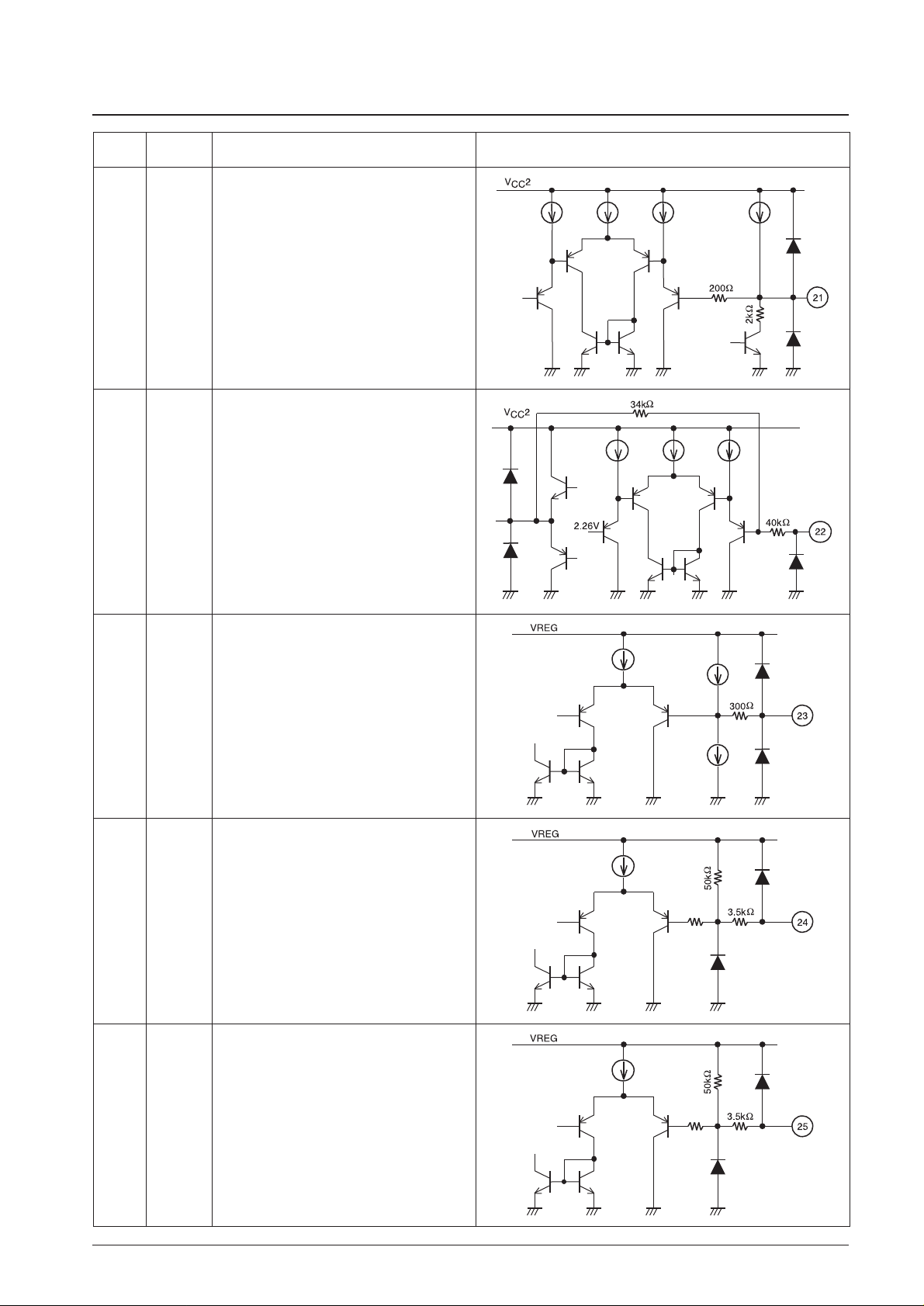
Pin to set the PWM oscillation frequency.
Connect a capacitor between this pin and GND.
Control voltage input pin. For control with this pin,
set the PWMIN pin to the L level.
Pin to set the operation time of motor lock protection
circuit and to set the initial reset pulse.
Connect a capacitor between this pin and GND.
When the protection circuit is not to be used,
connect a capacitor and resistor (150 kΩ, 4700 pF)
in parallel between this pin and GND.
Start/stop control pin.
Start with L and stop with H or in the open condition.
PWM pulse input pin.
Output drive with L and output OFF with H or in the
open condition. For control with this pin, apply the
voltage of VCTL2 voltage or more to the VCTL pin.
Continued from preceding page.
Continued on next page.
Page 9
No. 7104-9/17
LB11820M
Pin No.
26
27
28
29
30
Pin
F / R
HP
BR
REV
SEL
GND
Equivalent circuitFunction
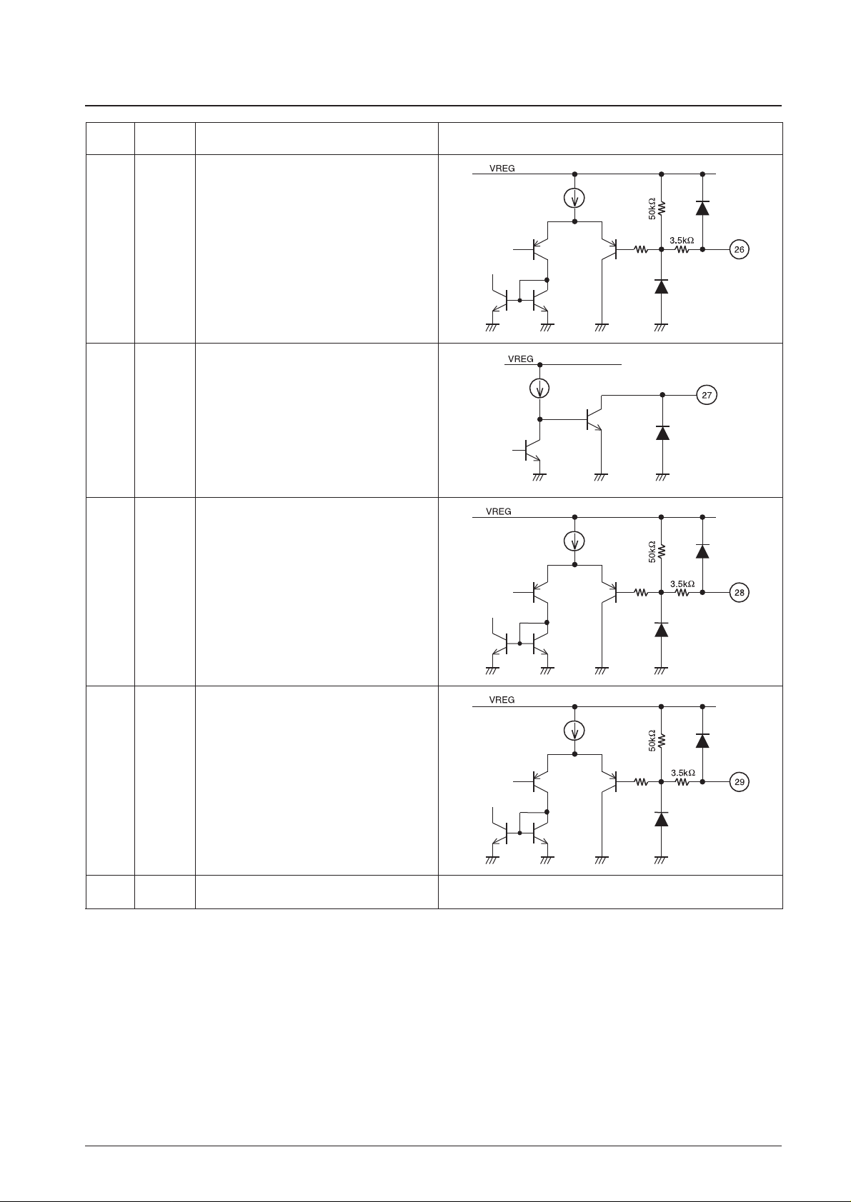
Forward/reverse input pin
Hall signal three-phase synthesis output signal
Brake input pin.
Brake with L and normal rotation with H or in the
open condition.
Reverse OFF selector pin.
Effective with L and ineffective with H or in the open
condition.
GND pin
Continued from preceding page.
Page 10
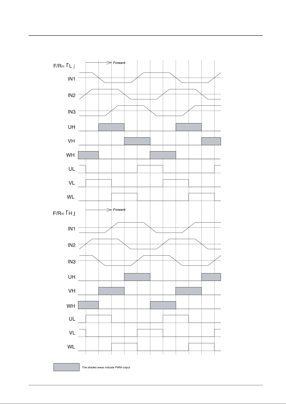
Hall Signal Input/Output Timing Charts
No. 7104-10/17
LB11820M
Page 11
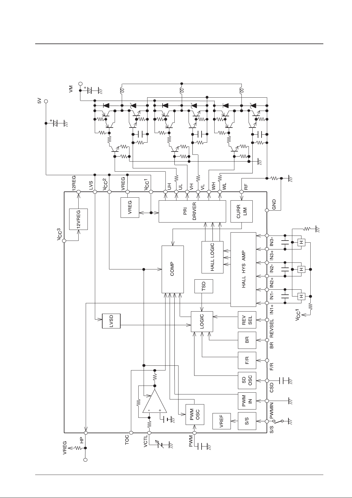
Sample Application Circuit
BIP Transistor Drive (upper side PWM) Using a 5 V Power Supply
No. 7104-11/17
LB11820M
Page 12
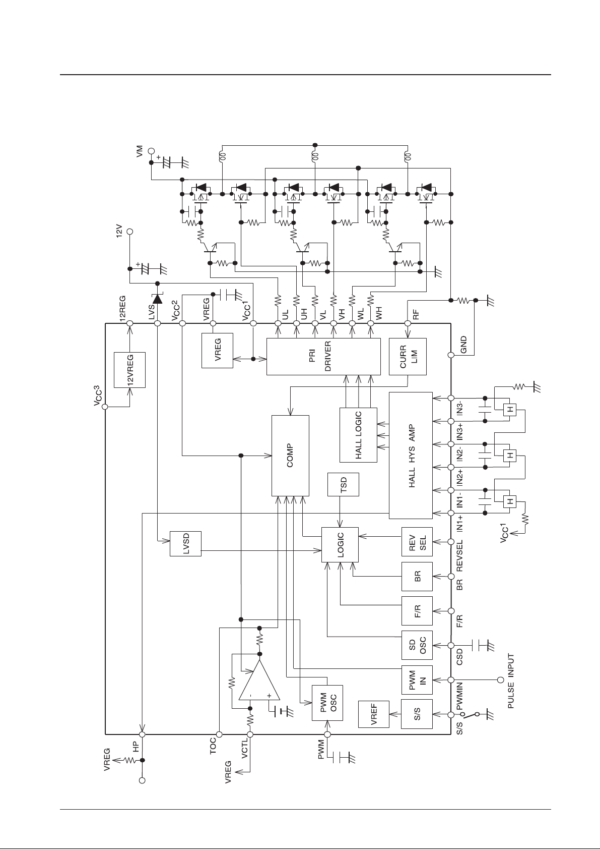
No. 7104-12/17
LB11820M
MOS Transistor Drive (lower side PWM) Using a 12 V Power Supply
Page 13
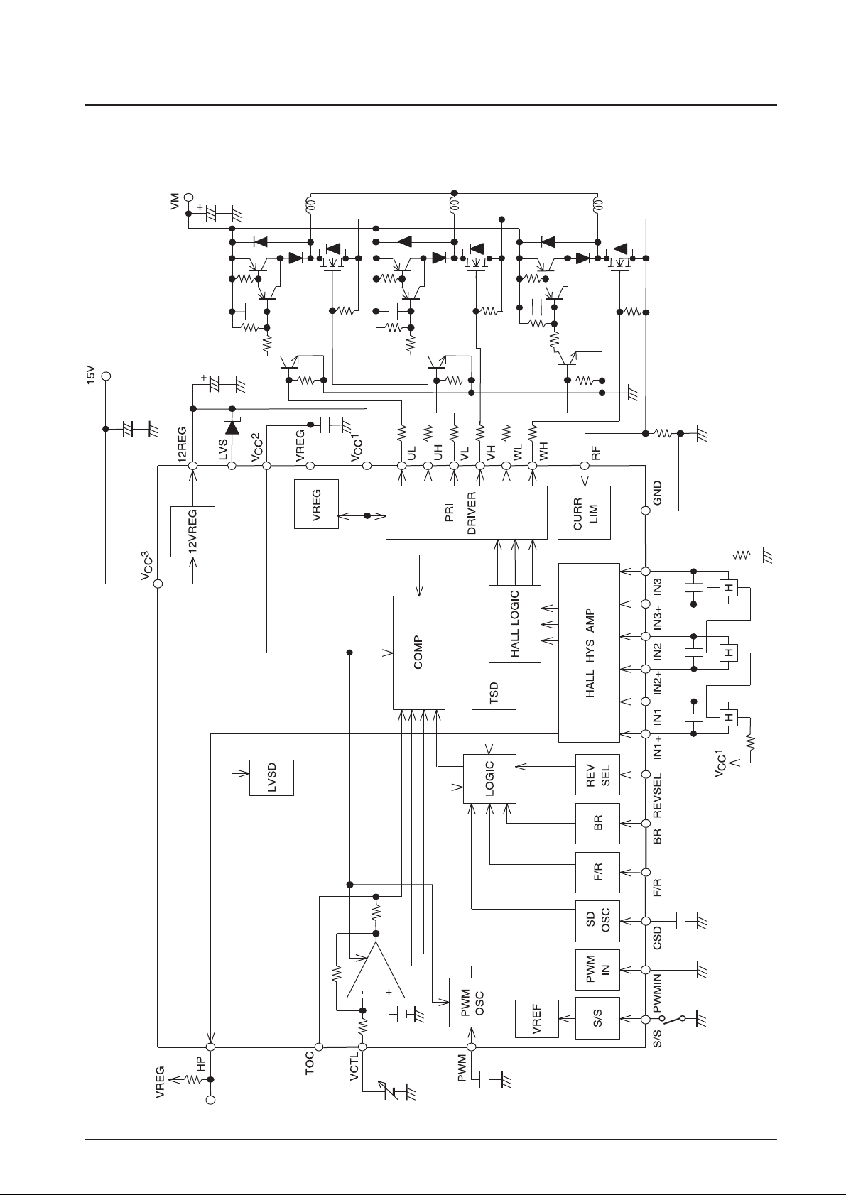
No. 7104-13/17
LB11820M
NMOS Transistor + PNP Transistor Drive (lower side PWM) Using a 15 V Power Supply
Page 14
No. 7104-14/17
LB11820M
Functional Description
1. Output Drive Circuit
This IC employs a direct PWM drive method to minimize the power loss at output. The output TR is normally
saturated in the ON condition, adjusting the motor drive power by changing the output on-duty. Output PWM
switching is made on UH, VH, and WH output sides. Since UL – WL and UH – WH outputs are of the same output
form, either lower PWM or upper PWM can be selected by changing the external output Tr connection method.
Selection of diode to be connected to the non-PWM side output requires attention because there is a problem of
reverse recovery time. (Unless a diode with the short reverse recovery time is selected, the through current flows in an
instant when the PWM side Tr is turned ON.)
UL – WL and UH – WH outputs enter the high impedance condition at a time of stop or when the supply voltage is
extremely low (below the allowable operation voltage). Accordingly, an appropriate measure (pull-down resistor, etc.)
is necessary in the external circuit to prevent an incorrect action due to the leak current.
2. Current Limiting Circuit
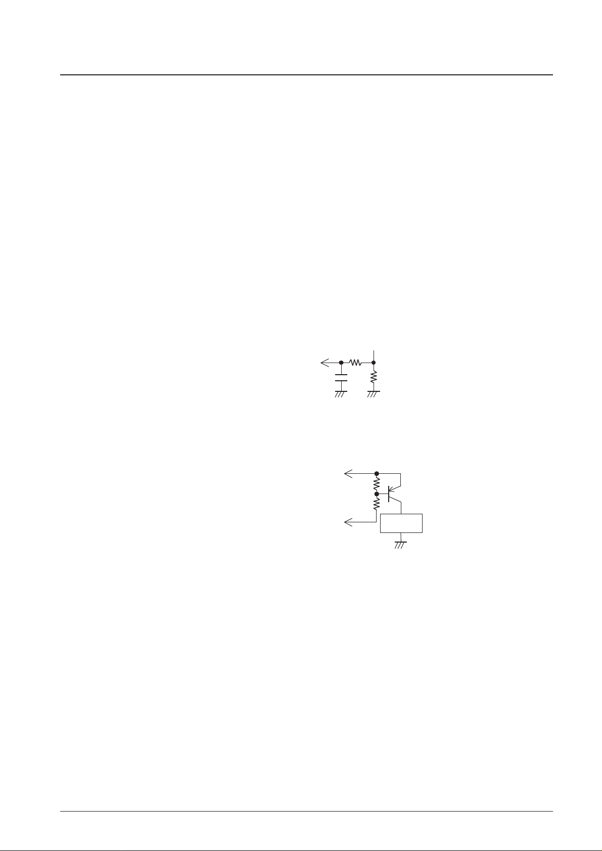
The current limiting circuit performs limiting with the current determined from I = VRF/Rf (VRF = 0.5 Vtyp,
Rf:current detector resistance) (that is, this circuit limits the peak current).
Limiting operation includes decrease in the output on-duty to suppress the current.
The current limiting circuit incorporates a filter circuit to prevent an incorrect action of current limiting operation due
to detection of the reverse recovery current of output diode during PWM operation. This internal filter circuit will be
enough to prevent trouble for normal application. In case of an incorrect action (diode reverse recovery current
flowing for 1 µs or more), add an external filter circuit (R, C low pass filter, etc.).
3. Power Save Circuit
This IC enters the power save condition to decrease the current dissipation in the stop mode. In this condition, the bias
current of most of circuits is cut off. Even in the power save condition, the 5 V regulator output (VREG) is given. If
the bias current of Hall device is to be cut, 5 V and Hall device may be connected via PNP Tr as a means to meet such
needs.
4. Compatibility with Various Power Supplies
To operate this IC with external 5 V power supply (4.5 – 5.5 V), short-circuit VCC1 and VREG pin for connection to
power supply.
To operate this IC with external 12 V power supply (8 – 13.5 V), connect power supply to VCC1 (5 V is generated at
the VREG pin to function as a power supply to the control circuit).
To operate this IC with external 15 V power supply (13.5 – 19 V), connect power supply to VCC3 and short-circuit
12REG and VCC1 pins (12 V is generated at the 12REG pin to function as a power supply to VCC1).
Connect the VCC2 pin basically to the VREG pin. In an application in which the motor rotation speed is to be
determined by the external fixed voltage (resistor division, etc.), set VCC2 to 12 V (by connecting to VCC1) to suppress
variation of the output duty. (Variation of IC is difficult to affect adversely because of increase in the PWM oscillation
amplitude and in the comparator dynamic range.)
5. PWM Frequency
PWM frequency is determined from the capacity C (F) of capacitor connected to the PWM pin.
fPWM ≈ 1 / (45000 × C)
Connection of a 1000 pF capacitor causes oscillation of about 22 kHz. Excessively low PWM frequency causes causes
a switching sound from the motor while excessively high PWM frequency causes increase in the power loss at the
output. About 15 – 50 kHz is recommended. Capacitor GND should be arranged near the IC GND pin as much as
possible to protect from the effect of output noise.
To pin RF
Current detection resistance
To pin VREG
To pin S/S
Hall device
Page 15
No. 7104-15/17
LB11820M
6. Drive Method
The output duty can be controlled according to any of following methods.
• Control with the VCTL pin voltage
For the control voltage, refer to the electric characteristics. For control with the VCTL pin, set the PWMIN pin voltage
to the L level.
• Control with the voltage applied to the TOC pin
The TOC pin voltage and PWM oscillation waveform are compared to determine the output duty. The output duty
becomes 0 % when the TOC pin voltage exceeds VOH(PWM) (3.0 V typ) and 100% when it becomes lower than the
VOL(PWM) (1.2 V typ). For control with the TOC pin, set the PWMIN pin voltage to the L level.
For control with the input level other than the internal CTL amp control input level, external connection of amp allows
setting to the arbitrary input level (with the external amp output connected to the TOC pin). For control from the TOC
pin, fix the VCTL pin voltage.
For an application in which the regulated voltage is applied to the TOC pin through resistor division, etc., it is
necessary to take into account the effect of resistor (about 20 kΩ) incorporated between the TOC pin and CTL amp
output. (Variation about ±20%, temperature characteristics about +0.3%/°C). If the noise is included in the voltage to
be applied to the TOC pin, chattering may occur in the output. In this case, stabilization with a capacitor is necessary.
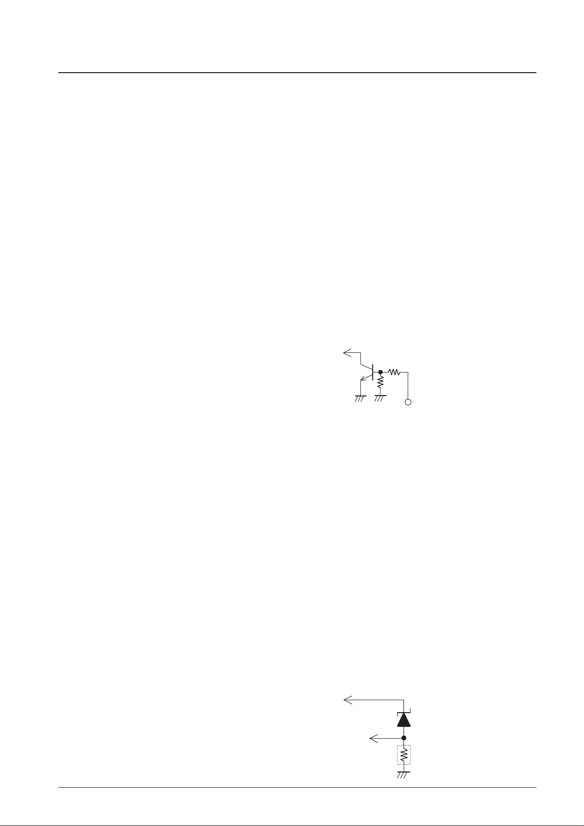
• Pulse control with the PWMIN pin
The output can be controlled on the basis of duty obtained by entering the pulse in the PWMIN pin. The output can be
turned ON when the L-level input voltage is applied to the PWM pin and OFF when the H-level input voltage is
applied. With the PWMIN pin open, the output becomes the H level and is turned OFF. If input with reversed logic is
necessary, addition of external Tr (NPN) may be enough.
For control with the PWMIN pin, set the VCTL pin voltage that is more than the VCTL2 voltage (output duty set to
100%) or connect the TOC pin to GND.
7. Hall Input Signal
The Hall input requires the signal input with an amplitude exceeding the hysteresis width (50 mV max). Considering
the effect of noise and phase displacement, the input with the amplitude of 120 mV or more is recommended.
When the noise causes disturbance in the output waveform (at a time of phase change) or HP output (Hall signal threephase synthesis output), insert a capacitor to the input to prevent such trouble. The Hall input is used as a signal to
determine the input to the restriction protection circuit and the protection circuit during reverse. Though noise is
ignored to a certain degree, due attention must be paid when using these protection circuits.
When all three phases of Hall input signal are entered, the output is turned OFF entirely (all of UL, VL, WL, UH, VH,
and WH OFF).
To enter the Hall IC output, fix one side of input (+ or –) to the voltage within the common-mode input range for Hall
device. This will allow input from 0 to VCC1 for another single-side input.
8. Circuit for Low-Voltage Protection
This circuit detects the voltage applied to the LVS pin. When this voltage drops below the operation voltage (see the
electric characteristics), the one-side output (UH, VH, and WH) is turned OFF. To prevent repetition of output ON/OFF
near the protection activation voltage, the hysteresis is provided. Accordingly, the output is not recovered unless the
voltage rises by about 0.5 V above the activation voltage.
The protection activation voltage is for the 5 V system detection level. The detection level can be raised by connecting
the zenor diode in series to the LVS pin and by shifting the detection level. The LVS pin inrush current at a time of
detection is about 65 µA. To stabilize rise of the zenor diode voltage, increase the diode current by inserting the
resistor between the LVS pin and GND.
When the protection circuit is not used, apply a voltage on a level where the protection is not activated, instead of
setting the LVS pin open (output OFF with the pin open).
To pin PWMIN
Pulse input
To detection power supply
To pin LVS
Page 16

No. 7104-16/17
LB11820M
9. Motor Lock Protection Circuit
A motor lock protection circuit is incorporated for protection of IC and motor when the motor is locked. When the
Hall input signal is not changed for a certain period with the motor driving, the one-side output (UH, VH, WH) is
turned OFF. The time is set by means of a capacity of a capacitor connected to the CSD pin.
Set time (s) ≈ 154 × C (µF)
Addition of a 0.01 µF capacitor causes a protection time of about 1.54 seconds. (Drive is turned OFF when one cycle
of Hall input signal is longer than this time period.) The time to be set must have a sufficient allowance so that the
protection is not activated at a normal motor startup. Select the capacitor of 4700 pF or more. The protection circuit is
not activated when braking. To cancel the restriction protection condition, one of following steps must be taken:
• Stop mode (10 µs or more)
• Maintaining the output duty 0% condition through input of VCTL or PWMIN for more than the period of tCSD × 2.
(tCSD(s) ≈ 0.5 × C (µF). When the 0.01 µF capacitor is added, maintaining for about 10 ms or more is necessary.)
• Re-application of power supply
The CSD pin acts also as an initial reset pulse generation pin and causes reset of the logic circuit when connected with
GND. Accordingly, the motor drive condition can not be obtained. When this pin is not to be used, a resistor of about
150 kΩ and a capacitor of about 4700 pF must be connected to GND in parallel. When the restriction protection circuit
is not used, following functions are also invalid:
• Protection circuit for the reverse mode
• Overheat protection circuit
10. Protection Circuit at Reverse
This circuit becomes effective when the REVSEL pin is set to the L level. When this protection is not necessary,
either connect it to the VREG pin or keep it open.
When this circuit is effective, all outputs are OFF (all of UL, VL, WL, UH, VH, and WH OFF) when the drive is
OFF (output duty 0%). If the condition is switched rapidly from the output drive condition to the drive OFF
condition, the current flowing through the motor is returned to the power supply (the coil current flows through
output upper and lower diodes to power supply). If this current causes a trouble, such as rise of the supply voltage,
etc., it is necessary to reduce the duty in steps, instead of shutting of the drive suddenly.
Reverse condition is detected according to the input sequence of Hall signals (IN1, IN2, and IN3). When using this
protection circuit, it is necessary to connect the Hall device with motor while considering the Hall input sequence.
(See the three-phase logic truth table.) Reversing is judged when the Hall input is reversed by more than 120 degrees
in the electrical angle. The drive is not shut OFF immediately after judgment of reverse, but the drive is continued for
a certain period (equal to the motor lock protection set time) after drive start. If the reversing condition continues for
a certain period (equal to the set time of motor lock protection), the drive is shut OFF (all OFF).
When the motor is reversing before it is driven, the drive is continued for a certain period (equal to the set time of
motor lock protection). If the motor does not return to forward rotation within this period, the drive is shut OFF (all
OFF).
To cancel the protection, one of following steps must be taken:
• Stop mode (10 µs or more)
• Maintaining the output duty 0% condition through input of VCTL or PWMIN for more than the period of tCSD ×
2. (tCSD(s) ≈ 0.5 × C (µF). When the 0.01 µF capacitor is added, maintaining for about 10 ms or more is necessary.)
• Re-application of power supply
11. Overheat Protection Circuit
One-side output (UH, VH, WH) is turned OFF when the junction temperature (Tj) exceeds a specified temperature
(TSD). Since the minimum variation of TSD is 125°C, thermal design must be made so that Tj = 125°C is not
exceeded except in the case of abnormality. Accordingly, Pdmax whenTj(max) = 125°C is 0.72 W (Ta = 25°C).
When the motor lock protection is not to be used by inserting in parallel the resistor of about 150 kΩ and capacitor of
about 4700 pF between the CSD pin and GND, this overheat protection circuit does not function.
In this case, Tj(max) = 150°C, so that Pdmax = 0.9 W (Ta = 25°C).
Page 17

PS No. 7104-17/17
LB11820M
This catalog provides information as of June, 2002. Specifications and information herein are subject to
change without notice.
Specifications of any and all SANYO products described or contained herein stipulate the performance,
characteristics, and functions of the described products in the independent state, and are not guarantees
of the performance, characteristics, and functions of the described products as mounted in the customer’s
products or equipment. To verify symptoms and states that cannot be evaluated in an independent device,
the customer should always evaluate and test devices mounted in the customer’s products or equipment.
SANYO Electric Co., Ltd. strives to supply high-quality high-reliability products. However, any and all
semiconductor products fail with some probability. It is possible that these probabilistic failures could
give rise to accidents or events that could endanger human lives, that could give rise to smoke or fire,
or that could cause damage to other property. When designing equipment, adopt safety measures so
that these kinds of accidents or events cannot occur. Such measures include but are not limited to protective
circuits and error prevention circuits for safe design, redundant design, and structural design.
In the event that any or all SANYO products (including technical data, services) described or contained
herein are controlled under any of applicable local export control laws and regulations, such products must
not be exported without obtaining the export license from the authorities concerned in accordance with the
above law.
No part of this publication may be reproduced or transmitted in any form or by any means, electronic or
mechanical, including photocopying and recording, or any information storage or retrieval system,
or otherwise, without the prior written permission of SANYO Electric Co., Ltd.
Any and all information described or contained herein are subject to change without notice due to
product/technology improvement, etc. When designing equipment, refer to the “Delivery Specification”
for the SANYO product that you intend to use.
Information (including circuit diagrams and circuit parameters) herein is for example only; it is not
guaranteed for volume production. SANYO believes information herein is accurate and reliable, but
no guarantees are made or implied regarding its use or any infringements of intellectual property rights
or other rights of third parties.
12. Forward/Reverse Rotation
To select forward or reverse in the rotation condition, a measure is taken to prevent flow of the through current
(through current due to the output Tr OFF delay time at selection) at the output. Selection during rotation causes the
current exceeding the current limit value to flow through the output Tr because of the motor coil resistance and motor
reverse electromotive voltage condition. It is therefore necessary to select the external output Tr that is not damaged
by this current or to select forward/reverse only when the motor rotation speed has decreased to a certain level.
13. Brake operation
Braking is made by setting the BR pin to the L level. Braking consists of a short-circuit brake condition in which all
of one-side outputs (UH, VH, or WH) are turned ON while other outputs (UL, VL, WL) are turned OFF. A measure
is taken to prevent flow of through current (through current due to output Tr OFF delay time at selection) when the
brake is operated or cancelled. While braking is made, current limiting and motor lock protection circuits are not
operative.
Short-circuit braking causes large current to flow through the output Tr because of motor coil resistance and the motor
reverse electromotive voltage condition during operation. It is therefore necessary to select the external output Tr that is
not damaged by this current or to activate braking only when the motor rotation speed has decreased to a certain level.
14. Power Supply Stabilization
This IC is of a switching drive type and the power line tends to be affected. It is therefore necessary to connect a
capacitor of sufficient capacity for stabilization between the VCC1 pin and GND.
To insert a diode in the power line to prevent breakdown through reverse connection of power supply, the power line
becomes more readily affected. It is necessary to select a larger capacity.
To turn ON/OFF the power supply with a switch, etc., large distance between the switch and capacitor causes
substantial deviation of the supply voltage due to the line inductance and inrush current into the capacitor. In certain
cases, the withstand voltage may be exceeded. In this case, do not use a ceramic capacitor whose series impedance is
low. Instead, use an electrolytic capacitor to suppress the inrush current and to prevent voltage rise.
15. VREG Stabilization
To stabilize the VREG voltage that is the power supply for the control circuit, connect a 0.1 µF or more capacitor between
VREG and GND. The capacitor GND must be wired near the GND pin of IC as much as possible.
 Loading...