

Page 1

LAN83C175
ADVANCE INFORMATION
LAN83C175 - EPIC/C
Ethernet CARDBUS Integrated Controller With
Modem Support
FEATURES
• IEEE 802.3 Compliant 10/100 Mb/s
Ethernet Controller
• Fully Compliant Glueless Integrated
CardBus Interface
• Secondary 8 Bit interface to Support Multifunction CardBus Adpaters Including LAN /
Rockwell or Lucent Modem Combinations
• Supports 3.3V or 5V Modem and Physical
Layer Interface
• 10Base-T Physical Layer Digital Support
- Smart Squelch Digital Noise Filter and
Receive and Collision Input to Reject
Both Analog and Digital Noise on
Twisted Pair Receive Inputs
- 10Mbps Manchester Encoding /
Decoding with Receive Clock
Recovery
- Automatic Polarity Detection
- Full Duplex Support
• Scatter/Gather DMA Capability
• Supports Chaining of Transmit Packets
• Optional Early Transmit and Early Receive
• Optional Receive Lookahead Buffering
Mode
• 4.5Kbyte On-Chip Receive Buffer and
1.5Kbyte On-Chip Transmit Buffer
Eliminate Bus Latency Issues
• Automatic Rejection of Runt Packets
• Automatic Retransmission of Collision
Frames from Internal Buffer
• Automatic Padding of Short Frames
• Big or Little Endian Byte Ordering
• Capable of Supporting 64Kbyte Expansion
Boot ROM
• IEEE Standard MII Interface to Physical
Layer
• Interface to LAN83C694 Shares MII Pins
• Serial MII Management Interface
• Interface to an 8 Bit Parallel EEPROM for
Storage and Retrieval of LAN Address and
Configuration Information
• On-Chip Clock Multiplier
• Low Power Sleep Mode and Extended
Power Management Features
• Internal and External Loopback Diagnostic
Functions
• Simple I/O Pin Mapping Scheme to
Facilitate In-Circuit Test
• Single 3.3V Supply
• 208 Pin TQFP Package
Page 2

2
TABLE OF CONTENTS
FEATURES........................................................................................................................................1
GENERAL DESCRIPTION .................................................................................................................3
PIN CONFIGURATION.......................................................................................................................5
DESCRIPTION OF PIN FUNCTIONS .................................................................................................6
FUNCTIONAL DESCRIPTION............................................................................................................9
DMA OPERATION............................................................................................................................11
TRANSMIT DMA ..............................................................................................................................11
RECEIVE DMA.................................................................................................................................17
TRANSMIT/RECEIVE ARBITRATION FOR CARDBUS BUS...............................................................25
BIG/LITTLE ENDIAN SUPPORT....................................................................................................... 25
MAC OPERATION................................................................................................................................ 28
MAC RECEIVER..................................................................................................................................28
MAC TRANSMITTER........................................................................................................................30
MII MANAGEMENT INTERFACE ......................................................................................................32
EEPROM INTERFACE..................................................................................................................... 32
POWER DOWN MODE....................................................................................................................34
JUMPER OPTIONS..........................................................................................................................34
SOFT RESET...................................................................................................................................34
CONFIGURATION ...........................................................................................................................35
MAPPING OF ROM AND CONTROL FUNCTIONS.........................................................................................35
REGISTER MAP/CONTROL REGISTER DECODE..........................................................................................37
REGISTER DESCRIPTIONS/CONTROL REGISTERS .....................................................................38
MODEM AND EXTERNAL FLASH RAM INTERFACE AND CONTROL...........................................64
MODEM REGISTERS MAP .............................................................................................................64
MODEM REGISTERS BITS DESCRIPTION...................................................................................................65
PHYSICAL CONNECTION........................................................................................................................68
MODEM AND RAM ACCESS TIMING.........................................................................................................68
OPERATIONAL DESCRIPTION....................................................................................................... 69
MAXIMUM GUARANTEED RATINGS........................................................................................................... 69
DC ELECTRICAL CHARACTERISTICS........................................................................................................ 69
TIMING DIAGRAMS ........................................................................................................................71
80 Arkay Drive
Hauppauge, NY. 11788
(516) 435-6000
FAX (516) 273-3123
Page 3

3
GENERAL DESCRIPTION
The LAN83C175 EPIC/C is a high-performance
Low CPU Utilization Ethernet network controller
designed to interface directly to the CardBus
Local Bus on one side and to the 802.3 standard
Media Independent Interface (MII) on the other
side. The network interface can also be
configured to communicate directly with the
LAN83C694 10BASE-T transceiver.
The LAN83C175 implements 802.3 Media
Access Control functions. It is capable of
running at Ethernet rates of both 100Mbps and
10Mbps. An MII compliant serial management
interface is provided to control external media
dependent transceivers. The LAN83C175 is a
two channel bus master (one for transmit, one
for receive) capable of transferring data at the
maximum CardBus transfer rate of 132Mbps.
The LAN83C175 has several features designed
to maximize throughput and minimize CPU
utilization, including the optional Receive
Lookahead Buffering Mode, which eliminates the
need to re-copy the data from one host memory
location to another.
The LAN83C175 also includes a secondary
general purpose 8-bit interface with appropriate
registers, address lines and control lines. This
secondary interface provides all of the signals
required to implement a secondary function on
a CardBus adpater. An example of such a
secondary function is a 33.6Kbps or higher
speed modem design based on a Rockewell or
Lucent modem chip set.
Page 4

4
Cardbus
Epic/C
Cardbus
Interface
RINGIN
RINGOUT
MPWRDWN
MRESET_N
MCS_N
MA(15:0)
MD(7:0)
MA(x:0)
RDYMRDYM
AUDIOAUDIOIN
RINGIN
RINGOUT
PWRDWN
HINTIREQM
~RESET
~HCS
HA(x:0)
HD(7:0)
WR_N
RD_N
RAMCS_N
Physical Layer
Interface
PHY
FIGURE 1 - LAN83C175 SYSTEM DIAGRAM
~HWT
~HRD
Modem
ADDR(15:0)
DATA(7:0)
RAMWE_N
RAMOE_N
RAMCS_N
RAM
Page 5

5
PIN CONFIGURATION
5354555657585960616263646566676869707172737475767778798081828384858687888990919293949596979899
100
101
102
103
104
VDD
3.3
GND
N/C
AUDIOOUT
VDD
3.3
CAD24
nCBE3
GND
CAD23
CAD22
CAD21
VDD
3.3
CAD20
CAD19
GND
CAD18
CAD17
GND
CAD16
nCBE2
VDD
3.3
nCFRAME
nCIRDY
GND
N/C
nCTRDY
nCDEVSEL
VDD
3.3
nCSTOP
nCBLOCK
GND
nCPERR
nCSERR
VDD
3.3
CPAR
nCBE1
GND
VDD
3.3
CAD15
CAD14
GND
CAD13
CAD12
VDD
3.3
CAD11
N/C
GND
CAD10
CAD9
CAD8
VDD
3.3
GND
208
207
206
205
204
203
202
201
200
199
198
197
196
195
194
193
192
191
190
189
188
187
186
185
184
183
182
181
180
179
178
177
176
175
174
173
172
171
170
169
168
167
166
165
164
163
162
161
160
159
158
157
VDD
PHY
GND
RX_CLK
VDD
3.3
RX_DV
RX_ER
MDATA
GND
MCLK
PHYRST
TX_EN
GND
TXD3
TXD2
GND
TXD1
TXD0
VDDPHY
GND
RXD3
RXD2
VDD
PHY
RXD1
RXD0
CRS
N/C
N/C
FETPWRM
POWERDWNM
nRESETM
RINGOUT
nROMCS
nCSM
N/C
VDD
3.3
nMEMRD
nMEMWR
VDD
MOD
RINGIN
AUDIOIN
IREQM
GND
RDYM
MD7
MD6
GND
MD5
MD4
MD3
MD2/JMP2
GND
VDD
MOD
PHY
VDD
TX_CLK
FETPWR_PHY
ZENER
CLK25IN
nPHY_PWRDWN
694nEN
VDD
694nLNK
CBCLK
nCCLKRUN
nCGNT
nCREQ
CAD31
CAD30
CAD29
CAD28
CAD27
CAD26
CAD25
STATCHG
GND
COL
GND
VDD
VDD
BIAS
GND
GND
TEST
GPIO1
GPIO2
VDD
GND
GND
nCINT
nRST
GND
VDD
GND
VDD
GND
VDD
GND
VDD
GND
VDD
GND
1
2
N/C
3
4
5
6
7
X20
8
3.3
9
3.3
10
11
12
13
14
15
16
17
PHY
18
19
20
21
22
N/C
23
3.3
24
25
26
27
28
29
30
3.3
31
32
33
34
35
3.3
36
N/C
37
38
39
40
3.3
41
42
43
44
45
3.3
46
47
48
49
50
3.3
51
52
LAN83C175
208 Pin TQFP
156
155
154
153
152
151
150
149
148
147
146
145
144
143
142
141
140
139
138
137
136
135
134
133
132
131
130
129
128
127
126
125
124
123
122
121
120
119
118
117
116
115
114
113
112
111
110
109
108
107
106
105
MOD
VDD
GND
N/C
MD1/JMP1
MD0/JMP0
MA15
MA14
N/C
MA13
MA12
3.3
VDD
MA11
GND
MA10
MOD
VDD
MA9
MOD
VDD
MA8
GND
MA7
MA6
GND
MA5
MA4
GND
MA3
MA2
MA1
MA0
N/C
GND
3.3
VDD
GND
N/C
3.3
VDD
CAD0
CAD1
GND
CAD2
CAD3
GND
3.3
VDD
CAD4
CAD5
GND
CAD6
N/C
3.3
VDD
CAD7
nCBE0
GND
3.3
VDD
Page 6

6
DESCRIPTION OF PIN FUNCTIONS
TQFP PIN NO. NAME I/O DESCRIPTION
30 CBCLK I
28 nRST I
39,40,42,44,45,47,48,58
CAD[31:0] IOCBCardBus Multiplexed Address/Data Bus
,
61-63,65,66,68,69,71,
91,92,94,95,97,100-102,
108,111,113,114,117,
118,120,121
59,72,88,107 nCBE[3:0] IO
87 CPAR IO
74 nCFRAME IO
75 nCIRDY IO
78 nCTRDY IO
81 nCSTOP IO
82 nCBLOCK I
79 nCDEVSEL IO
35 nCREQ O
33 nCGNT I
84 nCPERR IO
85 nCSERR ODCardBus System Error (Open Drain)
27 nCINT ODCardBus Interrupt (Open Drain)
32 nCCLKRUN IO
151,150,148,147,145,
MA[15:0] O
143,141,139,137,136,
134,133,131-128
165,164,162-159,
MD[7:0] IO
153,152
173 nMEMRD O
172 nMEMWR O
177 nROMCS O
5 TX_CLK I
198 TX_EN O
196,195,193,192 TXD[3:0] O
CardBus Clock
CBCLK
CardBus System Reset
CB
CardBus Multiplexed Command/Byte
CB
Enable Signals
CardBus Parity Signal
CB
CardBus Cycle Frame Signal
CB
CardBus Initiator Ready Signal
CB
CardBus Target Ready Signal
CB
CardBus Cycle Stop Signal
CB
CardBus Lock Signal
CB
CardBus Device Select
CB
CardBus Bus Request
CB
CardBus Bus Grant
CB
CardBus Parity Error
CB
CardBus Clock Control and Request Line
CB
Address Bus to Modem and Flash RAM.
TTL4
Data Bus to EEPROM
TTL4
External Bus Read Signal
TTL4
External Bus Write Signal
TTL4
Flash RAM Chip Select
TTL4
MII Transmit Clock
TTL4
MII Transmit Enable
TTL4
MII Transmit Data
TTL4
Page 7

7
TQFP PIN NO. NAME I/O DESCRIPTION
206 RX_CLK I
184 CRS I
189,188,186,185 RXD[3:0] I
4 COL I
204 RX_DV I
203 RX_ER I
200 MCLK O
202 MDATA IO
19 694nLNK I
17 694nEN O
MII Receive Clock
TTL4
MII Carrier Sense
TTL4
MII Receive Data
TTL4
MII Collision Signal
TTL4
MII Receive Data Valid Signal
TTL4
MII Receive Error Signal
TTL4
MII Management Interface Clock
TTL4
MII Management Interface Data
TTL4
10Base-T Link Integrity Status
TTL4
694 Enable. Tri-States 694 Outputs when
TTL4
PHY100 is in use
14 CLK25IN I
21 GPIO1 IO
22 GPIO2 IO
20 TEST I
8 X20 O
System Clock (25MHz) Input
TTL4
General Purpose I/O
TTL4
General Purpose I/O
TTL4
Used for In-Circuit Device Test
TTL4
20MHz Buffered Clock Output
TTL4
11 BIAS I Bias Current Input for Clock Multiplier.
Connect a 6KΩ 1/8 w 1% Resistor between
RBIAS and Ground
12 ZENER I Regulated Voltage Input for Clock
Multiplier
199 PHYRST O
15 nPHY_PWRDWN O
6 FETPWR_PHY O
179 nRESETM O
176 nCSM O
166 RDYM I
Reset Output to Physical Layer Chip
TTL4
Physical Layer Power-Down Control
TTL4
Physical Layer Power-Down Control
TTL4
MODEM RESET
TTL4
MODEM chip select
TTL4
MODEM ready/busy signal. Ready when
TTL4
high
168 IREQM I
180 POWERDWNM O
181 FETPWRM O
170 RINGIN I
178 RINGOUT O
50 STATCHG O
MODEM Interrupt request
TTL4
MODEM Power Down
TTL4
MODEM Power Down Control
TTL4
MODEM Ring-in signal
TTL4
MODEM Ring-out signal
TTL4
CardBus status changed signal
TTL4
Page 8

8
TQFP PIN NO. NAME I/O DESCRIPTION
169 AUDIOIN I
Audio input to the chip
TTL4
56 AUDIOOUT O Audio output to CardBus
9,10,24,31,36,41,46,
VDD
3.3
PWR Connect to 3.3V Power Supply
51,53,57,64,73,80,86,
90,96,103,105,109,
115,122,125,146,174,
205
1,18,187,191,208 VDD
PHY
PWR Must be connected to the same power
supply as the Physical Layer device
140,142,156,157,171 VDD
MOD
PWR Must be connected to the same power
supply as the Modem and the External
Flash RAM. Note that the modem and
Flash RAM should operate at the same
voltage.
2,7,13,16,25,26,29,
GND PWR Connect to Ground
34,38,43,49,52,54,60,
67,70,76,83,89,93,99,
104,106,112,116,119,
124,126,132,135,138,
144,155,158,163,167,
190,194,197,201,207
3,23,37,55,77,98,110,
N/C No connects
123,127,149,154,175,
182,183
Page 9

9
FUNCTIONAL DESCRIPTION
The LAN83C175 EPIC/C is a high-performance
Ethernet network controller designed to interface
directly to the CardBus Local Bus on one side
and to the 802.3 standard Media Independent
Interface (MII) on the other side. The network
interface can also be configured to
communicate directly with the LAN83C694
10BASE-T transceiver.
The LAN83C175 implements 802.3 Media
Access Control functions. It is capable of
running at Ethernet rates of both 100 Mbps and
10 Mbps. An MII compliant serial
management interface is provided to control
external media dependent transceivers. The
LAN83C175 is a two channel bus master (one
for transmit, one for receive) capable of
transferring data at the maximum CardBus
transfer rate of 132 Mbps. Buffer format in host
memory is controlled by an independent linked
list structure for each channel.
The LAN83C175's architecture is essentially
broken into two independent transmit and
receive processes which share CardBus bus
and network bandwidth. This architecture is
ideal for full-duplex networks where
transmission and reception of frames may occur
simultaneously. An internal arbiter controls
which process has access to the CardBus bus
at a given time (see section on "transmit/receive
arbitration for CardBus bus").
The transmit process consists of a DMA
controller, local transmit RAM, memory transfer
unit ("MTU") and CSMA/CD transmit state
machine. The transmit DMA copies packet data
from host memory into the local buffer. When
ready, the memory transfer unit feeds data from
the transmit buffer to the CSMA/CD state
machine, which is responsible for sending data
out on the network under the Ethernet protocol.
When transmission is complete, the transmit
DMA posts the transmit status into host
memory, interrupts the host (optionally) and
looks for the next transmit packet to be queued.
Like the transmit process, the receive process
consists of a DMA controller, local receive RAM,
memory transfer unit and CSMA/CD state
machine. Packets are received by the
CSMA/CD state machine and stored into local
memory by the receive MTU. The receive DMA
then copies the data from the local buffer into
host memory, posts the receive status and
interrupts the host. The LAN83C175 has several
features designed to minimize CPU utilization,
including the optional Receive Look-ahead
Buffering Mode, which eliminates the need to recopy the data from one host memory location to
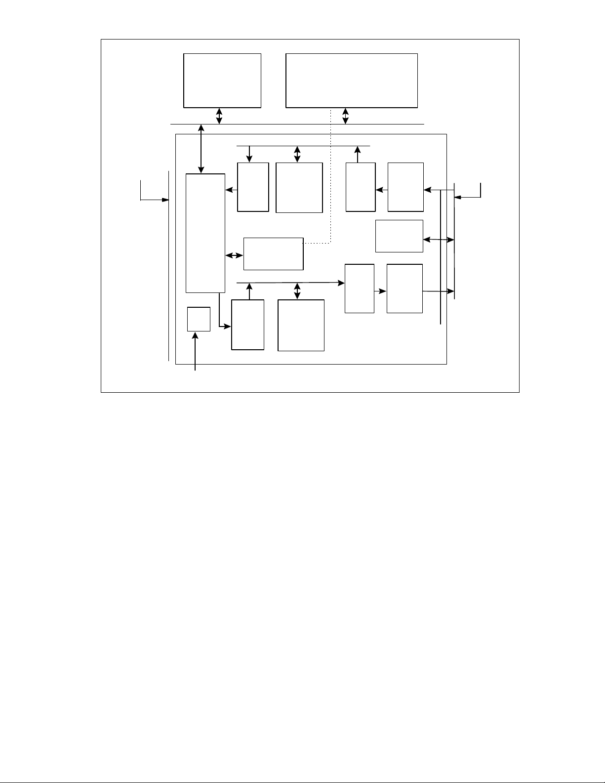
another. Figure 2 on the following page shows
a block diagram of the LAN83C175.
Page 10
10
SYS CLOCK
Flash EEPROM
for CIS and config.
Modem Chipset
Local Bus
32 bit Cardbus
BUS MASTER
SLAVE
PCI
INTERFACE
CLOCK
MULT.
PCI
RECEIVE
DMA
INTERNAL
RECEIVE
BUFFER
Receive
MTU
CSMA/CD
Management
Config and Status
REGISTERS
CSMA/CD
Transmit
PCI
TRANSMIT
DMA
Transmit
MTU
TRANSMIT
BUFFER
FIGURE 2 - EPIC/C BLOCK DIAGRAM
MII INTERFACE
Receive
MII
Page 11

11
DMA OPERATION
NEXT DESCRIPTOR ADDRESS
The software driver controls the transmit and
receive DMA controllers through the I/O control
registers and through "buffer descriptors" in host
memory. There is an independent chain (linked
list) of descriptors for each DMA. Each
descriptor may point to a single data buffer
(which can hold a whole frame or part of a
frame) or to a fragment list, which in turn
contains a list of buffers for an entire frame.
Each descriptor also contains control and status
information and a pointer to the next descriptor.
TRANSMIT DMA
The following diagram shows the format of the
transmit descriptor table:
DWORD 0 - Status
31 0
TX LENGTH TX STATUS
7 - DEFERRING: This bit is set when the interframe gap state machine is deferring. If the
PHY has asserted the collision line as a result
of jabber, this bit will stay set indicating the
jabber condition. Always returns 0.
6 - OUT OF WINDOW COLLISION: This bit is
set if a collision is detected more than one slot
time after the start of transmission.
Transmission is aborted under these conditions.
5 - COLLISION DETECT HEARTBEAT: This bit
is set to a '1' during transmission of each
packet. It is set to '0' if a collision is detected
within 36 bit times of the end of each packet
transmission. If no collision is detected within
this window, it remains '1'. This bit always
returns zero in full duplex mode.
4 - UNDERRUN: This bit is set when the
transmit DMA is unable to supply the transmitter
enough data to maintain frame transmission.
Always returns 0.
BUFFER ADDRESS
CONTROL BUF LENGTH
Bit Number and Description
31 through 16: Transmit Length
15 - OWNER: Descriptor ownership bit - set to
0 when the host owns the descriptor, 1 when
the NIC owns the descriptor.
14 and 13 - Reserved.
12 through 8 - COLLISION COUNT: These bits
contain the number of collisions detected while
attempting to transmit the current packet. Bit 12
also indicates transmit abort for excessive
collisions.
3 - CARRIER SENSE LOST: This bit is set if the
carrier is lost during packet transmission.
Carrier sense is monitored from its rising edge
at the start of the outgoing frame's echo.
Transmission is not aborted upon loss of carrier.
This bit will always return zero in full duplex
mode.
2 - TRANSMITTED WITH COLLISIONS: When
set, this bit indicates the frame collided at least
once with another frame on the network. It is not
set for either out-of-window collisions or
excessive collision aborts.
1 - NON-DEFERRED TRANSMISSION: This bit
is set if the frame is transmitted successfully
without deferring. A deferred transmission can
only occur the first time an attempt is made to
send a packet. Collisions are not deferred
transmissions.
0 - PACKET TRANSMITTED: This bit is set to
indicate transmission of a packet without
excessive collisions or abort.
Page 12

12
DWORD 1 - Data Buffer/Start of Fraglist Pointer
Bit Number and Description
31 through 0: Starting address of data buffer or
fragment list in host memory space. Fragment
list must be DWORD aligned. Data buffer may
be aligned on any byte.
early transmit threshold register (if early
transmit will be used), inter-packet gap program
register, interrupt mask register and general
control register. The software must also
program the CardBus Transmit Current
Descriptor Address Register (PTCDAR) with the
address in host memory where the first transmit
descriptor will be located.
DWORD 2 - Control/Data Length
Bit Number and Description
31 through 21 Reserved: Must always be set to
0.
20 - LASTDESCR: Indicates that this is the last
descriptor for the current transmit frame (Not
used when FRAGLIST = 1).
19 - NOCRC: Disable automatic CRC
generation for this packet when set.
18 - IAF: When set, interrupt after this frame is
transmitted.
17 - LFFORM: Fragment list format - A "1"
indicates that the data length field comes before
the pointer in the fragment list. "0" indicates
that the pointer comes before the data length.
16 - FRAGLIST: Indicates that this descriptor
points to a fragment list.
15 through 0 - Length of data buffer (Not used
when FRAGLIST = 1).
DWORD 3 - Next Descriptor Pointer
Bit Number and Description
31 through 2 - Starting address of next
descriptor in host memory space. Descriptors
must be DWORD aligned.
1 - 0: Unused.
The software driver initializes the transmit
process by writing the transmit control register,
To begin packet transmissions, the software
driver programs the transmit descriptor chain
with the appropriate number of entries and then
sets the TXQUEUED bit in the COMMAND
register.
Descriptor entries describe the location of
transmit data in host memory. Data for a single
transmit frame may not always be in a
contiguous block in host memory. Therefore,
the LAN83C175 allows the software to specify
multiple data buffers for each frame. Each
frame may be queued in one of two ways, both
of which may be used in the same descriptor
chain:
1) Direct Queuing Method (descriptors point
directly to the transmit data buffers):
One or more descriptors may be used to point
to a single frame. All descriptors must have the
FRAGLIST control bit set to 0. The first
descriptor must contain the transmit length for
the frame. The last descriptor for the frame
must have the LASTDESCR bit set to 1 and
contain the desired values for the TXIAF and
NOCRC control bits. When the TXQUEUED bit
is set, the transmit DMA will read the from the
location in host memory pointed to by its
Current Descriptor Address register. If the
ownership bit in the descriptor is equal to 1 then
the LAN83C175 will accept the descriptor and
update its Current Descriptor Address register
with the value in the Next Descriptor Address
field. Otherwise the TXQUEUED bit will be
cleared (and the transmit queue empty (TQE)
interrupt set) and the Current Descriptor
Address register will not be changed. The
Transmit Length field in the first descriptor will
Page 13

13
always contain the number of bytes to be
transmitted on the network, and not necessarily
the number of bytes in the transmit buffers. The
transmit DMA will begin copying data from the
location in host memory specified by the Buffer
Address field in the first descriptor. It will
compare the transmit byte count to the Data
Length field, and copy the lesser number of
bytes into the local transmit RAM. If early
transmit is enabled, the LAN83C175 will
automatically initiate transmission on the
network when the number of bytes specified in
the Early Transmit Threshold register have been
loaded into the transmit buffer.
If the transmit byte count is less than the Data
Length field, or the LASTDESCR bit is set, then
the frame copy is complete after the buffer has
been read. The LAN83C175 will initiate
transmission on the network if it has not already
done so.
If the Data Length field is less than the transmit
byte count and the LASTDESCR bit is not set,
then the LAN83C175 will attempt to read
another descriptor. The transmit DMA will
proceed as before, however this time it will not
read the Transmit Length field, but instead use
the remaining number of bytes in its transmit
byte counter (original byte count minus bytes
already copied). This process will continue until
a descriptor is read with the LASTDESCR bit set
or the transmit byte count reaches zero. If
LASTDESCR is set and the total number of
bytes copied do not add up to the transmit byte
count, then the transmit MTU will pad the frame
with random data after copying all of the valid
data out of the transmit RAM. The CSMA/CD
state machine will not append the automatically
generated CRC to the frame if NOCRC is set in
the last descriptor for the frame.
After the LAN83C175 has initiated the first
transmission, it will check to see if there are any
more frames in the transmit queue. If the
software does not have another frame ready for
transmission, then the ownership bit in the next
descriptor must be 0. If the ownership bit is 0,
then the LAN83C175 will clear TXQUEUED and
set the transmit queue empty interrupt. If the
ownership bit is 1, then the LAN83C175 will
begin copying the next frame into the local
transmit RAM. The DMA will continue copying
transmit buffers until the frame has been
completely loaded into the transmit RAM or the
first transmission has completed. If the copy
completes while the first transmission is still in
progress, then the LAN83C175 will stop and
wait. When the transmission is finished, the
LAN83C175 will post the status into the first
descriptor for that frame and immediately
initiate the second transmission. If the
transmission completes before the copy is done,
the LAN83C175 will pause after the current
transmit buffer has been copied and post the
status from the first frame. If the early transmit
threshold has already been exceeded then the
second transmission will be initiated
immediately. The transmit DMA will then
continue by reading the next descriptor for the
copy in progress.
When the transmit status is posted, the
ownership bit will be written as 0 to indicate that
the host now owns that descriptor again. The
Transmit Length field will not be overwritten. If
TXIAF is true in the last descriptor for the frame,
then the transmit complete (TXC) interrupt will
be set. When there are no frames left in the
queue and the last transmission has completed
on the network, the transmit DMA will set the
transmit chain complete (TCC) interrupt and
return to its idle state.
2) Fragment List Method (descriptor points
to a fragment list)
This method of queuing a transmit frame is
much like the first method, except that each
frame is always specified by one descriptor
which points to a list of buffers (fragment list)
instead of the buffers themselves. The
FRAGLIST bit in the descriptor must be set to 1
and the LFFORM bit must properly indicate the
format of the fragment list. The first entry in the
fragment list tells how many data buffers
Page 14

14
(fragments) are listed. Up to 63 fragments are
allowed. The remaining entries specify the
starting address and length of each buffer.
As in the direct queuing method, the transmit
DMA will copy fragments one at a time into the
local buffer until Transmit Length bytes have
been copied or all of the fragments have been
read. If early transmit is enabled, transmission
will be initiated when enough bytes have been
copied to meet the early transmit threshold.
Otherwise transmission will be initiated when
the entire copy is complete.
When more than one frame is queued, the
transmit DMA will begin copying a second frame
while the first is transmitting. It will continue
copying fragments until the entire frame is
loaded or the first transmission has completed.
If the copy completes while the first
transmission is still in progress, then the
LAN83C175 will stop and wait. When the
transmission is finished, the LAN83C175 will
post the status into the first descriptor and
immediately initiate the second transmission. If
the transmission completes before the copy is
done, the LAN83C175 will pause between
fragments to post the status and then resume
the copy. If the early transmit threshold has
already been exceeded then the second
transmission will be initiated immediately.
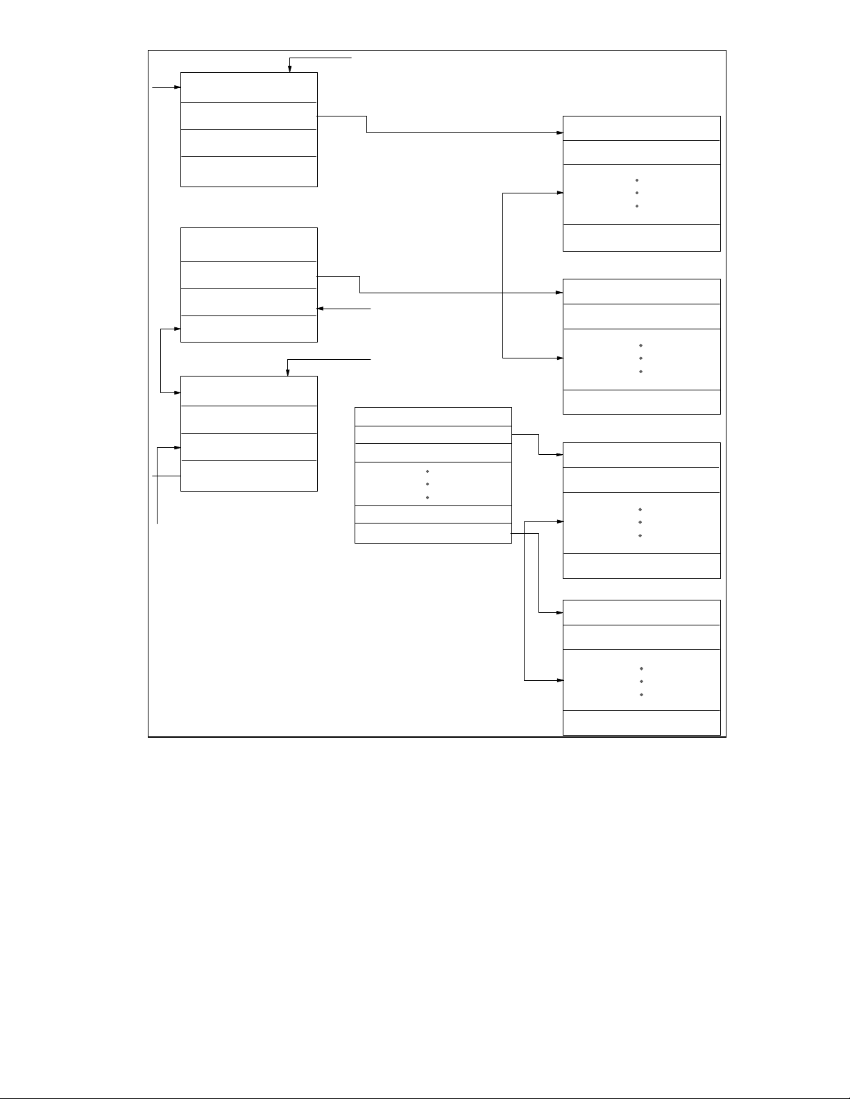
Figure 3 on the following page shows a drawing
of the Transmit Buffer Structure.
Page 15
15
TX LENGTH/STATUS
BUFFER ADDRESS
CONTROL/BUF LENGTH
NEXT DESCR. ADDRESS
TX LENGTH/STATUS
BUFFER ADDRESS
CONTROL/BUF LENGTH
NEXT DESCR. ADDRESS
TX LENGTH/STATUS
FRAME 1 STATUS
FRAME DATA
FRAME 1
FRAME DATA
LAST DESCR - 1
FRAME 2 STATUS
BUFFER ADDRESS
CONTROL/BUF LENGTH
NEXT DESCR. ADDRESS
FRAGLIST - 1
NUMBER FRAGS
PTR1(FRAG LENGTH)
FRAG LENGTH(PTR1)
PTRn(FRAG LENGTHn)
FRAG LENGTHn(PTRn)
FRAME 2
FIGURE 3 - TRANSMIT BUFFER STRUCTURE
FRAME DATA
FRAME DATA
Page 16

16
The software may add transmit frames to the
queue at any time. If the transmit process is
already running (TXQUEUED may still be set),
then all of the descriptor and fragment list
fields for the new frame must be valid
BEFORE the ownership bit in the first
descriptor is set. After the descriptors are
written, the TXQUEUED bit should be set.
TXQUEUED can be written regardless of
completion status and will ensure that the
latest frame is transmitted. If the LAN83C175
reaches the end of the transmit queue before
the new frame has been added, a transmit
chain complete interrupt is generated for the
old portion of the queue and another transmit
chain complete interrupt will be generated
when the added portion completes.
Interrupting Transmit Chain
The host may interrupt the transmit chain
before all frames have been transmitted by
setting the STOP_TDMA bit in the command
register. Setting this bit forces TXQUEUED to
0. The transmit DMA will finish copying any
frame that it has already begun, and transmit
all frames that have been loaded into the
transmit ram. After the transmit DMA has
posted the status for the last frame, it will set
the transmit chain complete interrupt and
return to its idle state (exactly as if the next
frame in the queue was owned by the host). If
the DMA reads a descriptor owned by the host
while a copy is still in progress, it will set the
transmit queued empty interrupt and wait for
the descriptor to be re-queued. It will not
return to the idle state until the copy is
completed.
Transmit Buffer Full
Whenever the local transmit RAM becomes
full, the transmit DMA will wait until more
space is available before loading any more
data. Space is freed up as the transmit MTU
reads data from the local RAM and updates its
pointers. In some cases, the transmit MTU will
leave its pointers at the beginning of a frame until
it knows that the transmission will not have to be
retried. Automatic retries can occur due to
collisions or early transmit underruns.
Transmit Underrun
A transmit underrun occurs in early transmit mode
when the transmit DMA can not keep up with
transmission on the network. Data must be read
from the local RAM before it is available. Usually,
when an underrun occurs, the transmit MTU will
generate a transmit underrun (TXU) interrupt and
update its transmit status register. The transmit
DMA will continue to operate as though nothing
has happened. The software driver will be
allowed to read the transmit status value from
TXSTAT and set the "transmit underrun go"
(TXUGO) bit to tell the MTU to retry the frame.
The MTU will re-transmit the entire frame out of
the local transmit ram. When transmission has
completed successfully, the DMA will post the
transmit status for the retry to the descriptor for
that frame. Operation will continue as it normally
would for a non-underrun situation.
The only exception to this behavior is when the
transmit MTU can not automatically retry an
underrun frame. This happens when the frame
size is larger than the transmit RAM (1.5 Kbytes)
and the transmit DMA has overwritten the
beginning of the frame before the underrun
occurs. If such an event occurs, the transmit
DMA will abort the copy and reset its pointers to
the first descriptor for that frame. The DMA will
clear the TXQUEUED bit and return to its idle
state. Transmit queue empty and transmit chain
complete interrupts will be generated along with
the transmit underrun interrupt. The software
driver must set TXUGO to reset the transmit MTU
and then set TXQUEUED if it wants to retry the
frame. The frame will be re-copied from scratch
out of host memory when TXQUEUED is set.
Page 17

17
Maximum Transmit Size and Burst Rate
Data Buffer Pointer
The transmit DMA supports frame sizes up to
64 Kbytes. The maximum size for a single
data buffer (fragment) is also 64 Kbytes. The
transmit DMA will run at the maximum
CardBus data rate of 132 MBytes/s when the
target memory system supports zero wait
state reads. The transmit DMA will burst as
many words as it can before having to
relinquish the CardBus bus. It is capable of
bursting data continuously with no wait states
(even when a transmission is active on the
network) until the transmit RAM becomes full.
The transmit DMA, however, will most likely
lose possession of the CardBus bus several
times before it can fill the entire 1.5 Kbyte
transmit buffer.
Bit Number and Description
31 Through 4 - Unused
5 through 0 - Number of fragments in this
fragment list (1-63). (Note: programming 0
into this field results in 64 fragments).
31 through 0 - Starting address of data buffer in
host memory space. Data buffer may be aligned
on any byte.
31 through 16 - Unused
15 through 0 - Length of data buffer.
RECEIVE DMA
The diagram below shows the format of the
receive descriptor table:
31 0
RX LENGTH RX STATUS
BUFFER ADDRESS
CONTROL
NEXT DESCRIPTOR ADDRESS
BUF LENGTH
Page 18

18
DWORD 0 - Status
Bit Number and Description
31 through 16 - RECEIVE FRAME LENGTH:
Number of bytes in the received frame.
2 - CRC ERROR: This bit is set when a frame's
computed CRC does not match the CRC
appended to the frame. If the frame is a runt, this
bit will be clear. In MII mode, this bit will also be
set if receive error was asserted on the MII
interface during reception of the frame.
15 - OWNER: Descriptor ownership bit - set to
“0” when the host owns the descriptor, set to
“1” when the NIC owns the descriptor.
14 - HEADER COPIED: Set when the receive
status is posted after a header copy.
13 - FRAGMENT LIST ERROR: Set when all
buffers in the fragment list have been filled
before the entire receive frame is copied.
12 - NETWORK STATUS VALID: Set when
bits 6 - 0 contain the status from the current
frame and bits 31-16 contain the frame length.
In the case of a header copy or fragment list
error, the receive status from the current
frame may or may not be posted. In all other
cases this bit will be set.
11 through 7 - Reserved
6 - RECEIVER DISABLED: This bit is set
when the receiver is in monitor mode. Always
returns 0.
5 - BROADCAST ADDRESS RECOGNIZED:
This bit is set when a broadcast address has
been recognized.
4 - MULTICAST ADDRESS RECOGNIZED:
This bit is set when a multicast address which
passes the hash filter has been recognized.
1 - FRAME ALIGNMENT ERROR: This bit is set
if a CRC error has occurred and the frame is not
byte aligned.
0 - PACKET RECEIVED INTACT: This bit is set
when a packet is received into the buffer space
without error.
DWORD 1 - Data Buffer/Start of Fraglist
Pointer
Bit Number and Description
31 through 0 - Starting address of data buffer or
fragment list in host memory space. Fragment
list must be DWORD aligned. Data buffer may
be aligned on any byte.
DWORD 2 - Control/Data Length (or Frame
Offset)
Bit Number and Description
31 through 19 - Reserved: Must always be set to
0.
18 - HEADER: Indicates that this descriptor is for
a header copy.
17 - LFFORM: Fragment list format - a 1 indicates
that the data length field comes before the
pointer in the fragment list. A 0 indicates that the
pointer comes before the data length.
3 - MISSED PACKET: This bit is set when a
packet with a recognized address and without
errors (or with masked errors) is not buffered
because the device is in monitor mode. This
bit is also set when the packet overflows the
receive buffer space and cannot be received.
Always returns 0.
16 - FRAGLIST: Indicates that this descriptor
points to a fragment list.
15 through 0 - Length of data buffer (when
FRAGLIST = 0) or Offset into frame where copy
begins (when FRAGLIST = 1).
Page 19

19
DWORD 3 - Next Descriptor Pointer
Bit Number and Description
31 through 2 - Starting address of next
descriptor in host memory space. Descriptors
must be DWORD aligned.
1 - 0: Unused.
The software driver initializes the receive
process by writing the receive control register,
interrupt mask register and general control
register. The software must also program the
CardBus Receive Current Descriptor Address
Register (PRCDAR) with the address in host
memory where the first receive descriptor will
be located.
To allow packet receptions, the software driver
programs the receive descriptor chain and
then sets the RXQUEUED and START_RX
bits in the COMMAND register. Setting
START_RX brings the CSMA/CD receiver
online. The receive DMA is enabled by setting
RXQUEUED. The software driver should set
RXQUEUED before or simultaneous to
bringing the receiver online so that the
receiver does not overflow the local buffer
while waiting for a descriptor to be queued.
The first descriptor must be valid before the
RXQUEUED bit is set. The first descriptor will
be read as soon as it is queued, even if no
receptions have occurred on the network.
The receive lookahead method offers
maximum performance in most cases.
Free Buffer Pool Method
In this mode the software driver pre-allocates
a pool of free buffers for frames received by
the LAN83C175. The ONECOPY bit in the
general control register must be set so that
the each frame may be copied into the buffer
pool without host intervention. The descriptors
for the free buffer pool may point directly to
the buffers, or point to a fragment list which in
turn specifies the buffers.
When the RXQUEUED bit is set, the receive DMA
will attempt to read the first descriptor from the
address pointed to by its Current Descriptor
Address register. If the ownership bit is 0, the
RXQUEUED bit will be cleared (and the receive
queue empty (RQE) interrupt set) and the Current
Descriptor Address register will not be changed.
If the ownership bit is equal to 1, the LAN83C175
will accept the descriptor and update its Current
Descriptor Address register with the value in the
Next Descriptor Address field. The LAN83C175
will save the descriptor information until a frame
is received. If the fraglist control bit is also 1, then
the receive DMA will read and save the address
pointer and data length for the first buffer in the
fragment list. The offset field in the descriptor
(see buffer length field) should be set to zero,
otherwise the copy will not begin at the start of the
frame. The fragment list format for the receive
DMA is identical to the format for the transmit
DMA.
As soon as a frame is received, the LAN83C175
will begin copying it from the local receive buffer
into the allocated buffer in host memory. If early
receive is enabled, the LAN83C175 can begin the
copy while reception is still in progress. The
receive DMA always monitors the local buffer
contents so that a receive underflow can never
occur. As soon as the receive DMA has copied
the number of bytes in the CardBus Receive Copy
Threshold register, it will set the receive copy
threshold (RCT) interrupt. When the receive DMA
has copied the entire packet from the local RAM
into host memory, it will post the receive status
into the first descriptor for the frame and set the
receive copy complete (RCC) interrupt. The DMA
will read the next descriptor and, if owned by the
NIC, check to see if there are any more frames to
copy out of the local RAM. If the receive DMA fills
the first host buffer before the entire frame has
been copied, it will read the next descriptor or
fragment list entry to find more buffer space. This
process will continue until the entire frame has
Page 20

20
been copied. If the DMA reads a descriptor
with the ownership bit set to 0, it will clear the
RXQUEUED bit (and set the receive queue
empty interrupt) and wait for a new descriptor
to be queued. In fragment list mode, the
receive DMA always expects the fragment list
to contain enough buffer space for the entire
frame.
If all the buffers in the fragment list are filled
before the copy is finished, then the DMA will
abort the copy and set the fragment list error
bit in the PRSTAT register. The DMA receive
status will be posted to the descriptor for that
frame and the RXQUEUED bit will be cleared.
If early receive is enabled, the network portion
of the receive status may not yet be valid, as
indicated by the RSV bit posted in the status.
The software driver may poll the RSV bit in the
interrupt status register, and when it returns a
1 read the receive status from PRSTAT. The
software may attempt to re-copy the frame by
setting the RXQUEUED bit again, or may
discard the frame by setting the NEXTFRAME
bit before or simultaneous to setting
RXQUEUED. If RXQUEUED is set after or
along with NEXTFRAME, the DMA will begin
to copy the next frame (if any) in the receive
buffer.
bit may be set at any time, even if the receive
DMA is still active.
Receive Lookahead Method
When this buffering method is used, the
LAN83C175 first copies only the header of a
frame into host memory, and then waits for a
queue from the software driver before copying the
rest of the frame. The software usually specifies
the final destination of the frame data with a
fragment list. The advantage to this buffering
method is that the LAN83C175 may copy frame
data to its final destination instead of a temporary
buffer space, so the software driver is not
required to re-copy the data from one host
memory location to another.
In receive lookahead mode, frames are usually
copied into the host memory one at a time, and a
handshake is performed between the software
driver and the LAN83C175 during each frame.
The handshake is performed using the
RXQUEUED and NEXTFRAME bits in the
COMMAND register, and the receive copy
complete (RCC) and header copy complete (HCC)
interrupts. The control bits in the receive
descriptors are also used to direct the receive
DMA.
Note: The DMA rounds the number of bytes
copied up to the nearest dword.
If the receive buffer does not start on a dword
boundary, then the number of bytes in the
receive buffer may be slightly less (up to 3
bytes) than the receive copy threshold when
the interrupt is generated.
Adding Receive Buffers to the Pool
The software driver adds buffers to the pool by
writing the appropriate descriptors and setting
their ownership bit to 1. If the receive DMA
has stopped (RXQUEUED is cleared), then the
software must set the RXQUEUED bit to
queue the new descriptors. The RXQUEUED
The software driver begins by setting up a buffer
for the header of the first frame and setting
RXQUEUED. The HEADER control bit in the
descriptor should be set and the FRAGLIST bit
should be cleared. The buffer address pointer
and length are specified directly in the descriptor.
When a frame is received, the receive DMA
begins copying the beginning of the frame into
the header buffer until the buffer is full, or until the
entire frame has been copied. The copy may
begin before the entire frame has been received if
early receive is enabled. When the header copy
is complete, the receive DMA status will then be
posted to the descriptor for the header buffer, and
the header copy complete interrupt will be set. If
reception from the network has completed, then
the network portion of the posted status will be
Page 21

21
valid, and the RSV bit will be set to 1. In early
receive mode, the receive DMA status may be
posted before the network status for the frame
is available, in which case the RSV bit in the
descriptor will be set to 0. If the entire frame
fits into the header buffer, then the network
receive status will always be posted with the
frame. After a header copy, the receive DMA
always clears the RXQUEUED bit (also setting
the receive queue empty interrupt, which may
be masked) and waits in the idle state for the
software driver to queue a fragment list for the
rest of the frame.
After examining the header data, the software
driver may discard the frame or have it copied
into host memory as many times as it would
like. The software requests copies of the frame
by programming descriptors (and fragments
lists) and setting RXQUEUED without setting
NEXTFRAME. The frame is copied exactly as
it would be in the free buffer pool mode, with
the exception that the offset field is used with
fragment list copies. The software may not
need all of the bytes at the beginning of the
frame to be copied, so it may specify an offset
into the frame where the copy should begin.
The offset field shares a location in the
descriptor with the buffer length field because
the buffer length is not specified in a descriptor
for a fragment list. The receive DMA copies
the frame into host memory beginning from
the byte number specified in the offset. If the
offset field is not zero, then the copy will not
begin until the entire frame has been received
from the network, even if early receive is
enabled. This is so that the receive DMA does
not copy invalid data if the offset is greater
that the number of bytes that have been
received so far. Usually, the entire frame will
have been received before the fragment list is
available.
When the copy is finished, the receive status
is posted and the receive copy complete
interrupt is set. The receive DMA will then
read the next descriptor, and if the ownership
bit is set it will immediately begin to copy the
same frame into host memory again. If the
descriptor is owned by the host, then
RXQUEUED will be cleared (and receive queue
empty interrupt set) and the receive DMA will wait
in the idle state for another command. If the
software driver wants another copy of the frame, it
may queue another descriptor and set
RXQUEUED without setting NEXTFRAME. This
procedure will be repeated until the software
chooses to go on to the next frame.
The software driver discards a frame by setting
NEXTFRAME before or simultaneous to setting
RXQUEUED. If RXQUEUED is set after or along
with NEXTFRAME, the receive DMA will begin to
copy the next frame (if any) in the receive buffer.
The next descriptor queued should contain a
header buffer for the next frame.
Occasionally, the software driver may want to
discard a frame immediately after reading its
header, but still read the receive status for that
frame. If the valid network status is not posted in
the descriptor, then the software driver may read
it from the PRSTAT register. The driver must
first set NEXTFRAME and RXQUEUED to
discard the frame, as described above. However,
the next descriptor in the receive descriptor list
must have the ownership bit cleared (host still
owns descriptor). This allows the LAN83C175 to
update the PRSTAT register without starting to
copy the following frame. The software driver
must poll the RQE (receive queue empty) interrupt
to determine when the status is available. When
the RQE interrupt is set, the driver may read the
receive status from the PRSTAT register. The
receive status valid bit in the interrupt status
register will not indicate when the receive status
is available.
When the software driver only wants one more
copy of the current frame, it does not have to wait
for the copy to complete before setting
NEXTFRAME. The software may set
NEXTFRAME immediately after setting
RXQUEUED (on the following I/O write) and begin
Page 22

22
to queue the header descriptor for the next
frame. After the header descriptor is queued,
the software may set RXQUEUED again to
guarantee that the header descriptor is
recognized. When the DMA is finished
copying the first frame, it will immediately read
the next descriptor and may begin copying the
next header without waiting for the software to
respond to an interrupt.
Note: Software must never set NEXTFRAME
more than once per frame. NEXTFRAME
may only be set when the copy is in
progress or has already been completed.
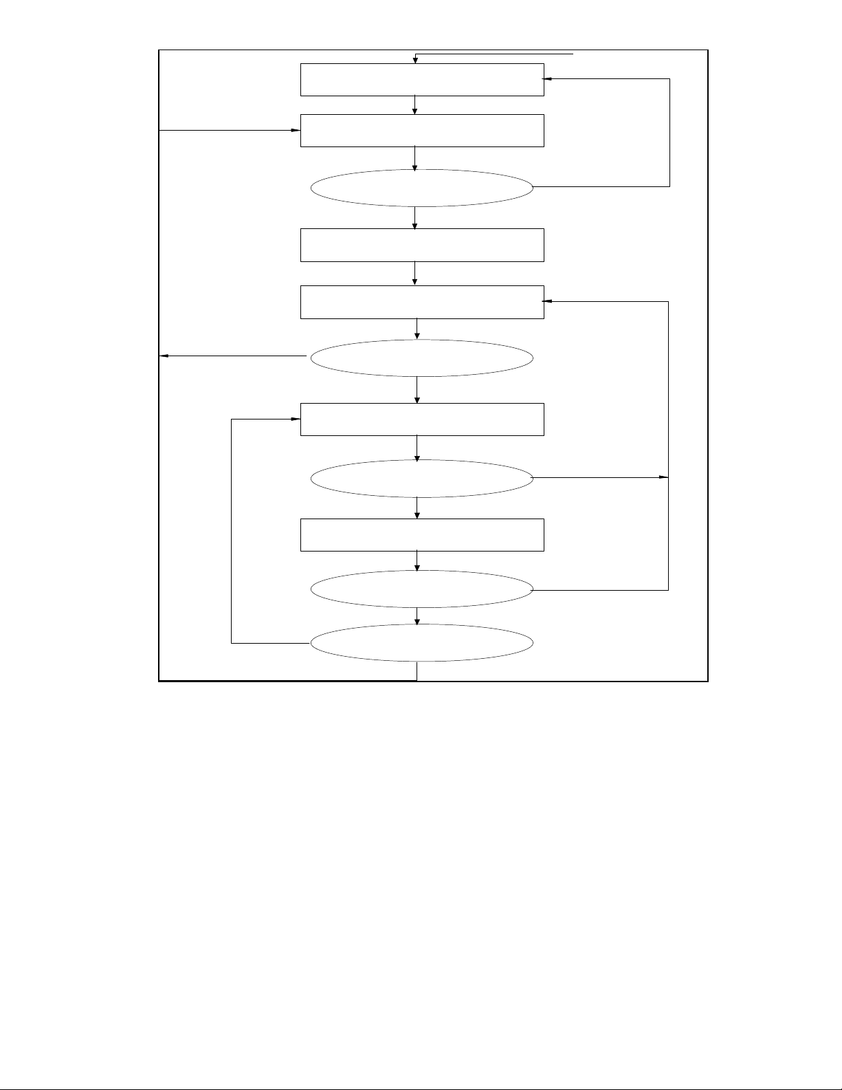
Figure 4 shows an example of the Receive Buffer
Structure, and Figure 4 shows a flow diagram for
the Receive Buffering Method.
Page 23
23
WAIT
READ DESCRIPTOR
RESET
RXQUEUED SET
HEADER BIT SET
GO TO NEXT
FRAME
TRUE
OWNER
NIC
COPY HEADER
POST STATUS
WAIT
NEXTFRAME
READ DESCRIPTOR
OWNER
NIC
COPY FRAME
POST STATUS
RDMA STOPPED
(RXQUEUED=0)
HOST/CLEAR RXQUEUED
DONE/CLEAR RXQUEUED SET HCC
RXQUEUED SET
FALSE
(HEADER BIT CLEARED)
HOST/CLEAR RXQUEUED
DONE/SET RCC
YES
NO
FALSE
NEXTFRAME
TRUE
FIGURE 4 - RECEIVE LOCKAHEAD BUFFERING FLOW
Page 24

24
Stopping the Receive DMA
Maximum Receive Size and Burst Rate:
The receive DMA may be halted by setting the
STOP_RDMA bit in the command register.
Setting this bit forces RXQUEUED to 0. The
CSMA/CD receiver should also be taken off-line
to prevent it from continuing to buffer receive
frames. The receive DMA will attempt to
complete any copy in progress. When finished,
it will return to its idle state. When the
CSMA/CD receiver is off-line and has also
returned to its idle state, the RXIDLE bit in the
interrupt status register will become true (1). If
the DMA reads a descriptor owned by the host
before it completes its current copy, it will set
the receive queued empty interrupt and return to
the idle state. The DMA will continue the copy
when more buffers are queued. The software
driver can tell if a copy is still in progress or
if there are any more frames in the local receive
RAM by reading the RCIP and RBE bits in the
interrupt status register.
The STOP_RDMA bit can be set when the
receive DMA has read and saved the
information in a descriptor, but there are no
frames in the local receive RAM. In this case,
the receive DMA will reset its current descriptor
pointer back to that descriptor and return to the
idle state. When the RXQUEUED bit is set
again, the DMA will be re-read the descriptor.
The receive DMA supports frame sizes up to 64
Kbytes. The maximum size for a single data
buffer (fragment) is also 64 Kbytes. The receive
DMA will run at the maximum CardBus data
rate of 132 Mbps when the target memory
system supports zero wait state writes. DMA
bursts at this rate will run for a limited number
of dwords. The length of each burst is
dependent on the FIFO threshold level and
access to the local receive RAM. The receive
DMA loads data into the receive burst FIFO at a
maximum rate of 100 Mbps (when reception is
not in progress) or 83 Mbps (when reception is
in progress). The receive DMA will
automatically initiate a burst on the CardBus
bus whenever the FIFO reaches programmed
threshold level. The receive DMA will continue
to load data into the FIFO while it is being
emptied onto the CardBus bus. The burst will
continue until the FIFO is empty or the receive
DMA loses control of the CardBus bus (to the
internal transmit DMA or to another CardBus
master). Another burst will begin when the
FIFO again reaches the threshold level, or when
the last of the data for the current copy has been
loaded into the FIFO. The CardBus bus will be
requested immediately if the receive DMA loses
possession of the bus while the FIFO is above
the threshold level.
THR_SEL
[1]
THR_SEL
[0]
THRESHOLD
LEVEL
0 0 1/4 Full (32
Bytes)
0 1 1/2 Full (64
Bytes)
1 0 3/4 Full (96
Bytes)
1 1 Full (128 Bytes)
Page 25

25
A lower threshold allows the LAN83C175 to
begin moving data on the CardBus bus sooner,
while a higher threshold may allow longer
bursts. A higher threshold level will not result in
parity generation and error detection. This block
is also responsible for responding to all slave
operations according to CardBus bus protocol
(including address recognition and parity
generation and error detection).
TRANSMIT/RECEIVE ARBITRATION FOR
CardBus BUS
Another major function of the CardBus Bus
Master/Slave Interface block is to arbitrate
between the transmit and receive DMA
controllers for access to the CardBus bus. Two
programmable priority select bits determine the
relative priority of each DMA controller. When
RXPRI is set, the receive DMA process may
preempt the transmit DMA process (when the
CardBus Latency Timer expires). The receive
DMA takes control of the CardBus bus if a
transmit fragment copy is suspended by a
target disconnect before the Latency Timer
expires. When RXPRI is cleared, the receive
process has to wait until the transmit DMA is
finished before it has access to the CardBus
bus. When TXPRI is set, the transmit DMA
process may preempt the receive DMA process
(when the CardBus Latency Timer expires). The
transmit DMA also takes control of the CardBus
bus if a receive fragment copy is suspended
by a target disconnect before the Latency
Timer expires. When TXPRI is cleared, the
transmit process has to wait until the receive
DMA is finished before it has access to the
CardBus bus. When both bits are set, either
process may preempt the other. When neither
bit is set, no preemptions occur. (Note:
Preemption does not occur when either process
has only one dword left to transfer).
SYSTEM ERRORS
There are four types of CardBus bus errors that
are considered fatal by the LAN83C175. They
are Master Abort, Target Abort, Address Parity
Error and Data Parity Error (see interrupt status
register for details). If any of these errors
occurs, the LAN83C175 will set the appropriate
interrupt and immediately discontinue all DMA
activity. The receiver will automatically be taken
off-line and any transmissions in progress will
be completed without a valid CRC appended (in
case transmit data was corrupted). Normal
operation may only be resumed by resetting the
LAN83C175 with the soft reset bit. The
software driver should make sure the transmitter
and receiver have returned to their idle states
(by polling the TXIDLE and RXIDLE bits in the
interrupt status register) before resetting the
device.
BIG/LITTLE ENDIAN SUPPORT
In order to run in Big Endian machines, the
LAN83C175 can be programmed to swap bytes
on the data bus in certain circumstances. In
Macintosh Power PC computers the bridge
between the Big Endian processor data bus and
the Little Endian CardBus bus swaps the order
of the bytes on the data bus (during data phase
only - addresses are never modified). This
means that byte size quantities transferred over
the data bus will always end up in the correct
location for their given address, but when 32 bit
(dword) quantities are transferred they will end
up with their bytes reversed.
When programmed into Big Endian mode,
the LAN83C175 will automatically swap the data
bytes internally when reading or writing
descriptor tables or fragment lists. This allows
the software driver to treat the descriptor and
fragment list entries as 32 bit quantities and not
worry about byte ordering.
Page 26

26
In order to comply with the CardBus
specification, the LAN83C175 will not swap the
data bytes on reads or writes to the
configuration or control register space. The
software driver will be responsible for correctly
interpreting the bytes when performing 32 bit
register read or writes on a Big Endian
machine.
When reading or writing Ethernet packet data,
the LAN83C175 will not perform any byte
swapping internally because the data on the
CardBus bus will already be in the correct order.
Page 27
27
3 2 1 0
31
0
Byte Transfer
Little Endian (PCI) Bus
PCI Bridge Action
0 1 2 3
7 0 7 0 7 0 7 0
Control Register dword transfer:
3 2 1 0
0 1 2 3
7
Descriptor/Fragment list dword transfer:
31 0
0 15 8 23 16 31 24
3 2
0 1 2 3
1 0
Big Endian (PowerPC) Bus
Byte Transfer
Little Endian (PCI) Bus
PCI Bridge Action
Big Endian (PowerPC) Bus
Byte Transfer
Little Endian (PCI) Bus
PCI Bridge Action plus
internal SMC91C120 swap
Big Endian (PowerPC) Bus
5
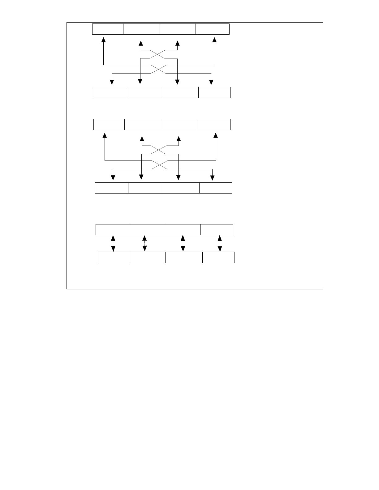
FIGURE 5 - LITTLE ENDIAN/BIG ENDIAN BYTE TRANSFER
The number in the box refers to the address of
the byte. The numbers above and below the
boxes refer to the bit number (the bit
ordering increases from LSB to MSB for both
formats, although some other documents
choose to label them differently).
Page 28

MAC Operation
The LAN83C175 is compliant with the 802.3
standard CSMA/CD protocol for 10 or 100
Mbps Ethernet networks.
MAC Receiver
The LAN83C175 CSMA/CD receiver is capable
of operating with network data rates of 10 and
100 Mbps. It supports current implementations
of 10 Mbps physical layer devices, and the
802.3u Media Independent Interface for 10 and
100 Mbps.
Basic Function
The receiver processes serial or nibble wide
data streams at data rates of 10 Mbps or 100
Mbps. The receiver detects start of frame,
provides destination address recognition and
filtering, transfers recognized frames to
memory, and provides error detection and
reporting.
Interface to Physical Layers
The receiver interfaces to the physical layer in
serial or parallel mode. When in the serial
mode, data is transferred serially on the RXD[0]
pin synchronous to the falling edge of the
receive data clock (RX_CLK). RX_CLK is a 10
MHz clock signal recovered by the physical layer
device from the data stream. The CRS and
COL signals provide carrier sense and collision
detect respectively.
In parallel mode, the physical layer device
transfers data to the LAN83C175 four bits at a
time on the RXD[3-0] data bus. The data is
transferred synchronously to the falling edge of
RXC. The signal Receive Data Valid (RX_DV)
informs the MAC of the RXD bus status. The
physical layer can also notify the LAN83C175 of
invalid data on the medium with the Receive
Error signal (RX_ER). Selecting the receiver
interface mode is performed by programming
the MII Configuration register.
Packet Reception/Serial Mode
After detection of carrier, serial bits received on
RXD[0] are synchronized to the rising edge of
RX_CLK. Each bit is shifted through an 8-bit
shift register scanning for a Start of Frame
Delimiter (SFD) pattern of '10101011' received
from left to right. Following detection of SFD, all
bits are byte aligned in the serial to parallel shift
register. Bits are received from least significant
bit to most significant bit within the byte. Data
from the shift register is transferred to the
receive FIFO where it waits for the receive DMA
to transfer it into local memory. The receive
process continues while CRS or COL are active.
Parallel Mode
Packet reception begins with the first nibble after
detecting RX_DV active. Nibbles transferred on
RXD[3-0] are synchronized to the rising edge
of RX_CLK and shifted into a 2-nibble shift
register. RXD[0] is the least significant bit
(LSB). SFD is detected when the shift register
contains the value '10101011' from LSB to
MSB. The preamble and SFD pattern received
from the PHY device is required to be nibble
aligned. Bytes are aligned in the 2-nibble shift
register after detection of SFD. Each byte is
transferred to the receive FIFO. Packet
reception continues while RXDV is active and
ends with the nibble preceding the falling edge
of RX_DV. While RX_DV is de-asserted, the
value of RXD[3-0] has no effect on the MAC.
Error Detection
The receiver computes the CRC of incoming
frames for all data following the detection of
SFD in both parallel and serial mode until the
end of frame, including the CRC field.
28
Page 29

Computation stops after the reception of the last
whole byte following loss of carrier in serial
mode or the transition of RX_DV from active to
inactive in parallel mode. The final value of the
CRC must be "C704DD7B" for the packet to be
validated. The CRC polynomial used is
AUTODIN II (X32 + X26 + X23 +X22 + X16 +
X12 + X11 + X10 + X8 + X7 + X5 + X4 + X2 +
X1 + 1).
In addition, in parallel mode, the receive error
signal, RXER, forces a CRC error when it is
asserted while RX_DV is active.
Address Recognition
When an address is recognized, the entire
frame will be saved into local memory.
Frame Processing
Frame processing begins following the detection
of SFD and continues until the last bit or nibble
of the frame has been received. Frame
processing counts the number of bytes in the
receive frame, transfers data to the receive
FIFO, checks for errors in both size and data,
posts status, generates interrupts, and counts
events. Frame processing can be controlled by
the receive control register to allow flexible
control of frame reception.
The receiver is capable of recognizing
individual, multicast, and broadcast addresses.
It can also be programmed to operate in
promiscuous mode and receive all frames
regardless of address. In all cases, address
recognition begins with the first byte following
SFD and ends with the sixth byte after SFD.
Individual destination addresses are compared
against a 6 byte register station address.
Multicast addresses are recognized by taking a
6 bit snapshot of the partially computed CRC
as the end of the destination address field
passes through the CRC checker. If the address
has the multicast bit set, the 6 bits are used
as a hashed index to a 64 bit Multicast Filter
table. If reception of multicast frames has been
enabled and if the 6 bit hash index points to a bit
in the table that has been set, the multicast
frame will be recognized. Broadcast frames are
received when the broadcast enable bit is set
and the destination address specifies a
broadcast frame, or when the hashed bit in the
Multicast Filter table has been set.
Reception of all multicast and broadcast frames
can be achieved by setting all bits in the
Multicast filter table and enabling reception of
multicast frames. If the address is not
recognized by any of the above means, then the
frame will be ignored.
Receive Byte Count
The receive byte counter begins counting with
the first byte of SFD and counts all bytes of the
frame until the end of frame is detected or an
error condition causes the frame processing to
be aborted. The counter filters runt frames by
comparing the current byte count value to the
slot time programmed in the Transmit Control
register. The frame is considered a runt until
the byte count exceeds the slot time value. Runt
frames are not received under default
conditions. Reception of runt frames can be
enabled by setting the receive runts bit in the
receive control register.
Data Transfer
Receive data is stored temporarily in a 8-dword
receive FIFO. Data begins to be stored in the
FIFO after detection of SFD. If the destination
address is not recognized, data stops being
transferred into the FIFO and the FIFO is reset.
When the FIFO level reaches 6-dwords, a burst
request to the local receive memory is made.
The return of acknowledge is guaranteed to
prevent the receive FIFO from overflowing. The
data path to the receive local memory is 32-bits.
29
Page 30

The data transfer process can be inhibited by
operating in monitor mode. This mode checks
validiity of incoming frames and maintains error
statistics, but does not store the frame in
memory. Frames which would otherwise have
been accepted cause the Missed Packet counter
to increment upon completion of the frame.
If the receive local memory becomes full during
reception of a frame, the frame is aborted. The
host is notified of the condition with an overflow
interrupt. Additionally, the missed packet
counter is incremented for each frame which
could not be received due to the overflow
condition.
Error Checking
saved due to an error or monitor mode, then the
contents of the status register will be lost after
the completion of the following packet. A
description of the status register contents is
located in the register definition section of this
data sheet.
Event Counters
Three event counters record CRC errors,
alignment errors, and missed packets. The
counters are all 8-bits wide and count from zero
to 255. At 255 the counters stop until they have
been read by the host. The counters are self
clearing after the read. The counters generate a
shared interrupt when any one of them reaches
a count of 192.
Received frames are checked for CRC and
alignment errors. If the CRC of a received
frame is incorrect, a CRC error is indicated in
the status register and the CRC error counter is
incremented. Reception of the frame is aborted
unless the receiver has been programmed to
receive errored packets. If the frame does not
terminate on a byte boundary and the CRC is
incorrect, then an alignment error is also
indicated in the status register. When this
occurs, the alignment error counter will be
incremented. A receive error interrupt is
generated when a CRC error is detected and
monitor mode is not set.
The receive control register can be programmed
to enable long frame checking (frames longer
than 1518 bytes). When a long frame is
detected the CRC and alignment counters are
not incremented.
Status
A status register is updated at the completion of
each frame whether it completed normally or
aborted in error. The status register holds
important information about the frame until it is
transferred with the packet data to the receive
local memory. If the frame data is not being
The counter is also incremented for receive local
memory full errors. The missed packet counter
is 8 bits wide and generates an interrupt when
it reaches a count of 192.
MAC TRANSMITTER
The LAN83C175 CSMA/CD transmitter is
capable of generating network data at rates of
10 and 100 Mbps. It supports current
implementations of 10 Mbps physical layer
devices, and the 802.3u Media Independent
Interface (MII) for 10 and 100 Mbps.
Basic Function
The transmitter generates serial and nibble
wide data streams at 10 or 100 Mbps. It forms
a proper preamble and SFD field at the
beginning of each packet. The frame data is
then shifted serially or by nibbles from an
internal transmit buffer to the physical layer. The
transmitter completes the packet by computing
and appending the CRC field. During packet
transmission, the transmitter monitors the
network for collisions and retransmits frames
after the a random backoff time when
necessary. The transmitter maintains the
transmit statistics and generates status
30
Page 31

information on each attempted transmission.
Optional operating modes can be selected by
programming the transmit configuration register.
Preamble Generation
At the beginning of each packet, the transmitter
generates 56 bits of preamble (an alternating
'1010' pattern). Following the preamble, a Start
of Frame Delimeter (a '10101011' sequence) is
transmitted.
Transmit Serializer
The transmit serializer converts 8 bits of parallel
data from the transmit buffer to serial or nibble
wide data. The mode of operation is selected
by the MII configuration register. In serial mode,
the transmit data is shifted out of the TXD[0] pin
synchronous to transmit clock. Data is shifted
out least significant bit (LSB) first. In nibble
mode, data is shifted synchronous to the
transmit clock at a one nibble per clock rate.
The data is transmitted least significant nibble
first on pins TXD[3-0]. The LSB is transmitted
on pin TXD[0].
Interframe Gap and Deference
Deference is initiated when both CRS and COL
have terminated at the end of a packet. The
transmitter deference logic initiates a 2-part
timer at the end of network activity. While this
timer is running, no frame transmission will be
initiated. The first part of the timer (interFrame
SpacingPart1) is used to observe the network
for transmission activity by other stations. If
this station is transmitting, carrier is sensed, or
collision is detected during this part of the timer,
the timer will be reset to zero and held there
until the termination of line activity. When the
first part of the timer elapses, line activity is no
longer observed and the timer runs to
completion.
If any frame is queued up for transmission at
the moment of timer expiration, transmission
will be initiated regardless of line activity.
The combination of interFrame SpacingPart1
and interFrame SpacingPart2 makes up the
Inter-Frame Gap (IFG) as defined by the 802.3
specification.
CRC Generator
The transmitter calculates the CRC and
appends it to each packet. CRC data is clocked
out most significant bit (MSB) first. A packet
can be transmitted without an attached CRC
field by programming the transmit descriptor.
This is provided for bridging applications in
which the original checksum must remain
attached to the packet until the final destination.
Transmit Protocol FSM
The transmit protocol FSM controls the
transmission of packets by monitoring
collisions, deferring to active carriers and
collisions, and initiating backoff when needed.
Collision Handling Logic
When collision is detected by the transmitter
section during the first slot timer of an active
transmission, the transmission terminates after
completion of the preamble and the jam
sequence. The jam sequence is 32 bits of logic
'1's. If collision is detected after the slot time is
passed, the transmission will be aborted after
the jam sequence. An out of window collision
interrupt will be generated and the collision
count status will be retained in the transmit
status register for software collection. After the
software has responded to the interrupt and reenabled transmissions, the transmit status will
be cleared and the packet will be automatically
retransmitted.
31
Page 32

Timers and Counters/Slot Timer
During transmit, the slot timer starts counting
once the receiver recognizes that a carrier is
present at the start of a returning preamble.
When backing off, the slot timer starts with the
end of transmit enable (TX_EN) for the collided
frame and is not reset by any other incoming
frames. The slot timer is programmable by the
transmit control register. The default slot time is
512 bit times.
Backoff Timer
After a transmission is terminated because of a
collision, a retransmission is attempted. The
backoff time is determined by the truncated
binary exponential backoff alogrithm. This
algorithm is:
draw random integer r: 0<=r<2**k
Where k equals the number of retries already on
this transmission. The value k is initialized to 0.
The required backoff time is 'r' number of slot
times. After the backoff time has been
completed, normal transmission deferral begins.
The backoff timer is a 12 bit counter that is
initialized to a random number when an
attempted transmission results in a collision.
The counter decrements once per slot time until
it reaches zero. The transmit protocol FSM
utilizes this timer to insert a variable amount of
delay ahead of its attempt to retransmit the
frame.
Collision Counter
Prior to the first attempt at each frame
transmission, the collision counter is initialized
to 0. Each attempted transmission of the frame
resulting in a collision causes the collision
counter
to increment. If the maximum number of
collisions (16) is reached before a successful
attempt to transmit the frame, the frame
transmission is aborted. An interrupt is
generated for an aborted frame indicating
transmission complete, and the collision count
value in the transmit status register is 16.
Heartbeat Detection
When the transmitter is configured in serial
mode, after each transmission, the transmit
logic opens a window 3.6 µsec long during
which it looks for a pulse on the COL pin. This
pulse is normally generated by the MAU and is
received through the MII interface. If the pulse
is received, the CDH status bit of the transmit
status register is cleared. If no pulse is received,
the CDH bit is set.
MII MANAGEMENT INTERFACE
The LAN83C175 supports the 802.3
specification for the MII Serial Management
Interface.
EEPROM INTERFACE
The LAN83C175 has a 8-bit parallel interface to
an external EEPROM. The parallel EEPROM
contains the LAN Address for the adapter and a
several bytes of configuration information. The
LAN address and configuration information is
automatically recalled from the first eight words
(each word is 16 bits) of the serial EEPROM
after reset. Access to the LAN83C175 is
disabled during the initial EEPROM recall. Any
attempted access results in a CardBus target
retry. The initial recall may be bypassed
through a test "jumper".
32
Page 33

EEPROM Format
The format of the EEPROM is shown in the
following Table. Note that this denotes only the
first 7 Dwords of the EEPROM. The CIS
Table 1 - EEPROM Format
DWORD BITS NAME
0 7-0 LAN Address Byte 0
0 15-8 LAN Address Byte 1
0 23-16 LAN Address Byte 2
0 31-24 LAN Address Byte 3
1 7-0 LAN Address Byte 4
1 15-8 LAN Address Byte 5
1 23-16 LAN Address Checksum
1 31-24 Board ID
2 7-0 Non-Volatile Control Ethernet
2 15-8 Non-Volatile Control Ethernet (15 unused)
2 23-16 Non-Volatile Control Ethernet (unused)
2 31-24 Non-Volatile Control Ethernet (unused)
3 7-0 Non-Volatile Control Modem
3 15-8 Non-Volatile Control Modem (15 unused)
3 23-16 Non-Volatile Control Modem (unused)
3 31-24 Non-Volatile Control Modem (unused)
4 7-0 CIS Address Ethernet
4 15-8 CIS Address Ethernet
4 23-16 CIS Address Ethernet
4 31-24 CIS Address Ethernet
5 7-0 CIS Address Modem
5 15-8 CIS Address Modem
5 23-16 CIS Address Modem
5 31-24 CIS Address Modem
6 7-0 Subsystem Vendor ID
6 15-8 Subsystem Vendor ID
6 23-16 Subsystem ID
6 31-24 Subsystem ID
7 7-0 PCI Minimum Grant Desired Setting
7 15-8 PCI Maximum Latency Desired Setting
registers for the modem and ethernet functions
are also located in this EEPROM at the
locations pointed to by the CIS pointer in each
of the function’s configuration space.
33
Page 34

The remaining words in the EEPROM are
available to software for general purpose nonvolatile storage. The eeprom can be accessed
through the base address designated by the
Expansion Rom Base Address in the
configuration space for both the modem and
ethernet function.
POWER DOWN MODE
The LAN83C175 has a power down feature
which allows it to consume less power when not
in use. The host may power down the
LAN83C175 by writing a 1 to the power down bit
in the general control register. When the bit is
set, the chip's internal system clock is gated off
to reduce switching current (the transmit and
receive clocks will be shut off internally if the
LAN83C175 is in loopback mode when power
down is set). While the LAN83C175 is powered
down, the host may read and write the
configuration registers or the general control
register. All other functions are disabled
(attempting any other operation will cause
unpredictable behavior). The power down bit
must only be set when the LAN83C175 is in its
idle state.
When the nRST pin is asserted, the LAN83C175
will automatically enter power down mode after
recalling the contents of the EEPROM. The
host may power up the LAN83C175 by writing a
0 to the power down bit. If the host wishes to
issue a software reset to the LAN83C175, the
power down bit must be cleared. When the
software reset has completed, the power down
bit will remain cleared and the LAN83C175 will
be ready to operate.
The power down bit does not affect the CardBus
clock inside the LAN83C175. Instead, the
LAN83C175 supports the CardBus clock run
function which allows the host system to slow
down or temporarily shut off the CardBus clock
at its source. The clock run function is
implemented according to the CardBus Mobile
design guide (revision 1.0).
JUMPER OPTIONS
There are several operational modes in the
LAN83C175 which are selected by "jumpers" at
power-up reset. Actual jumpers do not need to
be installed on the board. The options can be
set by external pull-up or pull-down resistors at
manufacturing time. Pins MD[2:0] are used to
make the jumper selections. The pins are
latched shortly after nRST goes inactive. The
jumpers are not sampled after soft reset. A pulldown resistor sets the jumper value to 0, and a
pull-up sets it to 1. The jumpers are defined as
follows:
MD[2] BYPASS EEPROM RECALL - When set
to 1, the EEPROM recall is not performed after
power-up reset. Used for test purposes only.
MD[1:0] These should be pulled down to 0.
SOFT RESET
The software driver may reset the LAN83C175
to its initial state by setting the soft reset bit in
the general control register. All state machines
and pointers to the internal RAMS will be reset.
Soft reset can only take place when the
LAN83C175 is powered up. Soft reset does
NOT affect the configuration of the LAN83C175.
The configuration registers (excluding EEPROM
control) will only be reset and the EEPROM will
only be recalled after hard reset.
Each time the software driver is loaded, it must
set soft reset before enabling the LAN83C175 to
act as a bus master. The driver may be loaded
after a warm boot, and the LAN83C175 DMA
controllers could be left in an unknown state.
If the LAN83C175 is enabled as a bus master
before a soft reset is issued, the DMA
controllers could corrupt host memory with a
bus master operation that was started before the
warm boot. When the soft reset bit is set, the
LAN83C175 takes 15 CardBus clocks to reinitialize itself. The device must not be
accessed within that time period.
34
Page 35

CONFIGURATION
The LAN83C175 is automatically configured by
the host system power-up software before the
machine is booted to an operating system.
Configuration is performed through the CardBus
configuration space. The LAN83C175 indicates
its requirements and the power-up software
allocates the appropriate resources. Note that
there is a separate configuration space for the
ethernet function and the modem function.
The LAN83C175 has the following requirements
for both the ethernet and modem functions:
A) 256 byte I/O space (may be mapped
anywhere in 32-bit I/O address space)
B) 4 Kbyte memory space (may be mapped
anywhere in 32-bit host memory space may be disabled on any host with I/O
space).
In machines with I/O space, mapping into
memory address space may optionally be
disabled by a bit in EEPROM. Any change in
the memory map enable bit will not take effect
until the system is reset (hard reset). The I/O
base address for the control registers will be
stored in the I/O Base Address Register (10h in
the configuration space). The memory base
address for the control registers will be stored in
the Memory Base Address Register (14h in the
configuration space). The I/O space is 256 bytes
long and is always naturally aligned. When
mapped into memory, the control registers
consume 4 Kbytes, even though only the first
256 bytes are used. They are always aligned to
a 4 Kbyte boundary. Access to the control
registers is enabled by the memory space and
I/O space enable bits in the CardBus Command
Register (04h in the configuration space). Both
memory space and I/O space will be disabled
after reset. All control registers are dword
accessible only.
C) 64 Kbyte expansion ROM space (may be
mapped anywhere in 32-bit host memory
space - will be disabled after boot
sequence).
D) Interrupt hardwired to CardBus nINTA line.
Because resources are relocatable, device
drivers must read the configuration registers
after boot time to determine where the device is
mapped.
Mapping of ROM and Control Functions
The LAN83C175 control registers are mapped
into both host I/O and memory space (to
accommodate host systems with no I/O space).
The expansion ROM is accessible when the
"address decode enable" bit in the ROM base
address register (30h in the configuration space)
is set and the memory space enable bit is set.
The ROM code is not executable in place. It
must be copied into system RAM and executed
from RAM (as per CardBus specification).
LAN83C175 control functions will not be
accessible through memory address space
while the ROM address decode enable bit is
set. Note that this ROM also contains the CIS
information for both the ethernet and modem
function.
When the expansion ROM is read, the
LAN83C175 will always return all four bytes in
the dword being accessed, regardless of which
byte enables are active.
The LAN83C175 will write to the flash ROM on a
byte basis, as decoded by the byte enables.
35
Page 36

ROM DECODE
ENABLE
1 X 1 1 Enabled I/O Space
1 X 1 0 Enabled Disabled
1 X 0 1 Disabled I/O Space
1 X 0 0 Disabled Disabled
0 1 1 1 Disabled I/O & Memory
0 1 1 0 Disabled Mem. Space
0 1 0 1 Disabled I/O Space
0 1 0 0 Disabled Disabled
0 0 X 1 Disabled I/O Space
0 0 X 0 Disabled Disabled
MEMORY
MAP ENABLE
MEM. SPACE
ENABLE
I/O SPACE
ENABLE
EXPANSION
ROM
CONTROL
REGISTERS
After reset, the ROM will be disabled and the
ROM base address will be unknown. The
system POST code will map the ROM into host
memory space, copy its contents into system
RAM and read the CIS structure or execute the
ROM initialization code The ROM must be found
since it contains the mandatory CIS structure for
CardBus functions. The ROM initialization code
is allowed to perform dynamic re-sizing of the
runtime code in order to use as little of the host
memory space as possible.
36
Page 37
Register Map/Control Register Decode
The following table shows the address mapping
of the LAN83C175 control registers. All
registers are dword accessible only.
Table 2 - Ethernet Function Control Register Map
00 COMMAND 40 LAN0
04 INTSTAT 44 LAN1
08 INTMASK 48 LAN2
0C GENCTL 4C ID/CHK
10 NVCTL 50 MC0
14 EECTL 54 MC1
18 PBLCNT 58 MC2
1C Reserved
4
5C MC3
20 CRCCNT 60 RXCON
24 ALICNT 64 RXSTAT
28 MPCNT 68 RXCNT
2C RXFIFO
4
6C RXTEST
30 MMCTL 70 TXCON
34 MMDATA 74 TXSTAT
38 MIICFG
3C IPG
1
1
78 TDPAR
7C TXTEST
1
1
1
1
1
1
1
1
1
4
1
4
80 PRFDAR
84 PRCDAR
88 PRHDAR
8C PRFLAR
90 PRDLGTH
94 PRFCNT
98 PRLCAR
9C PRLPAR
A0 PREFAR
4
A4 PRSTAT
A8 PRBUF
4
AC RDNCAR
B0 PRCPTHR
2
B4 F4 FEVTRMSKR
B8 F8 FPRSTSTR
4
BC PREEMPR
1
4
4
4
4
4
3
4
C0 PTFDAR
1
C4 PTCDAR
4
C8 PTHDAR
CC PTFLAR
4
D0 PTDLGTH
D4 PTFCNT
D8 PTLCAR
DC ETXTHR
E0 PTETXC
E4 PTSTAT
E8 PTBUF
4
EC PTFDAR2
1
F0 FEVTR
1
FC FFRCEVTR
Notes:
1
Used during initialization only (illegal to access when not idle).
2
Legal to access during transmit underrun only.
3
Legal to access only when frame is discarded after header copy and INTSTAT.RSV is 1.
4
Legal to access only in test mode.
1
1
4
4
4
4
4
1
4
4
4
4
37
Page 38

REGISTER DESCRIPTIONS/CONTROL
REGISTERS
00 - COMMAND
Reset Value: 0000000
31 through 8 - Reserved: These bits will return
unknown values and should never be written
to 1.
7 - TXUGO: This bit is set to restart
transmission after a transmit underrun error.
Setting this bit automatically clears the
transmit underrun interrupt. Writing a zero to
this bit has no effect. This bit always returns 0
when read.
6 - STOP_RDMA: This bit is used to halt the
receive DMA. Writing a 1 to this bit clears
RXQUEUED. Writing a 0 to this bit has no
effect. This bit always returns 0 when
read.
5 - STOP_TDMA: This bit is used to halt the
transmit DMA. Writing a 1 to this bit clears
TXQUEUED. Writing a 0 to this bit has no
effect. This bit always returns 0 when read.
2 - TXQUEUED: This bit is set to queue a
transmit descriptor. It will be cleared by the
LAN83C175 when it reads a descriptor that is still
owned by the host. Setting this bit automatically
clears the transmit queue empty interrupt.
Writing a 0 to this bit has no effect (in register test
mode writing 0 clears the bit). The host may clear
this bit by writing a 1 to TDMA_STOP.
1 - START_RX: Writing a 1 to this bit will bring
the LAN83C175 receiver online. When this bit is
cleared the receiver will stay online until the stop
bit is set.
0 - STOP_RX: Writing a 1 to this bit will take the
LAN83C175 receiver off-line. When this bit is
cleared the receiver will stay off-line until the start
bit is set.
04 - INTERRUPT STATUS
Reset Value: 01001100000000000000000
Bits in this register are set internally by the
LAN83C175. Bits are cleared by writing a 1 to
their respective locations. Writing 0 to a bit has
no effect (in register test mode writing 0 sets the
bit).
4 - NEXTFRAME: This bit is set by the host to
indicate that it does not need any more copies
of the current receive frame. The bit will be
cleared by the LAN83C175 the next time it
reads a descriptor. Writing a 0 to this bit has
no effect (in register test mode writing 0
clears the bit).
3 - RXQUEUED: This bit is set to queue a
receive descriptor. It will be cleared by the
LAN83C175 when it reads a descriptor that is
still owned by the host. Setting this bit
automatically clears the receive queue empty
interrupt. Writing a 0 to this bit has no effect
(in register test mode writing 0 clears the bit).
The host may clear this bit by writing a 1 to
RDMA_STOP.
31 through 28 - Unused
27 - PTA: CardBus Target abort - set when
EPIC/C cannot complete a bus master transaction
because target aborts the transaction.
26 - PMA: CardBus Master abort - set when
EPIC/C cannot complete a bus master transaction
because no target is found.
25 - APE: CardBus address parity error - set
when an address parity error occurs on the
CardBus bus while EPIC/C is not bus master.
This interrupt will only be set when the Parity
Error Response bit in the CardBus configuration
space is set.
38
Page 39

24 - DPE: CardBus data parity error - set
when a data parity error occurs on the
CardBus bus while EPIC/C is bus master.
This interrupt will only be set when the Parity
Error Response bit in the CardBus
configuration space is set.
23 - RSV: Receive status valid (read only does not generate an interrupt) - indicates that
the PRSTAT register contains valid status for
the frame currently being processed.
22 - RCTS: Receive copy threshold status
(read only - does not generate an interrupt) indicates that the copy in progress that has
passed the early receive copy threshold. This
bit returns zero when there is no receive copy
currently in progress or when the current copy
has not passed the threshold.
21 - RBE: Receive buffers empty (read only does not generate an interrupt) - indicates that
there is no data ready for copy in the receive
buffer.
20 - TCIP: Transmit copy in progress (read
only - does not generate an interrupt) indicates that a transmit DMA copy is partially
completed. The bit is set each time the
receive DMA begins to copy a frame. The bit is
reset after the copy completes and the status
is posted.
19 - RCIP: Receive copy in progress (read
only - does not generate an interrupt) indicates that receive DMA copy is partially
completed. The bit is set each time the
receive DMA begins to copy a frame. The bit
is reset after the copy completes and the
status is posted.
18 - TXIDLE: Transmit idle (read only - does not
generate an interrupt) - indicates that the NIC
transmitter and CardBus transmit DMA have
returned their reset states.
17 - RXIDLE: Receive idle (read only - does not
generate an interrupt) - indicates that the NIC
receiver and CardBus receive DMA have returned
their reset states.
16 - INT_ACTV: Interrupt active (read only - does
not generate an interrupt) - indicates that an
interrupt which is not masked is currently set.
This allows the host to read the interrupt status
through a register, even when interrupts are
disabled.
15 - GP2_INT: This interrupt becomes active
when the pin GPIO2) goes low. It is typically
used by the phy to indicate an event.
14-13 - Unused.
12 - FATAL_INT: This signal becomes true if any
fatal error occurs. These are DPE, APE, PMA,
and PTE. Note that these are also reflected in the
interrupt status word (27:24).
11 - RCT: Receive copy threshold crossed - set
when the receive copy in progress crosses the
CardBus receive copy threshold.
10 - PREI: This preemptive interrupt event
indicates that a packet is being received, with the
probability that by the time the host responds to
the interrupt, the packet will have been completely
received, reducing latency.
9 - CNT: Counter overflow - indicates that one of
the error counters is nearing its maximum count.
8 - Transmit underrun - set when an early transmit
underrun occurs. This interrupt is cleared
automatically when the TXUGO bit in the
command register is set. Clearing this interrupt
39
Page 40

manually (by writing to this register) does not
effect the TXUGO bit.
08 - INTERRUPT MASK
Reset Value: 000000000000000
7 - Transmit queue empty - set when NIC
reads a transmit descriptor that is still owned
by the host. This interrupt is cleared
automatically when the TXQUEUED bit in the
command register is set. Clearing this
interrupt manually (by writing to this register)
does not effect the TXQUEUED bit.
6 - TCC: Transmit chain complete - set when
the complete transmit chain has been
processed.
5 - TXC: Transmit complete - set when a
packet has been successfully transmitted or
aborted and the IAF bit is set for that frame.
4 - RXE: Receive error - set when a CRC error
occurs and Monitor mode is off.
3 - OVW: Receive buffer overflow warning set when a frame is received and local receive
buffer space is full.
2 - RQE: Receive queue empty - set when NIC
reads a receive descriptor that is still owned
by the host. This interrupt is cleared
automatically when the RXQUEUED bit in the
command register is set. Clearing this
interrupt manually (by writing to this register)
does not effect the RXQUEUED bit.
1 - HCC: Header copy complete - set when
receive frame header has been copied into
host memory.
0 - RCC: Receive copy complete - set when
receive frame has been copied into host
memory.
This register is used to enable certain interrupt
sources selectively. Bits that are 1 allow the
corresponding interrupt to cause an interrupt
request. Bits that are 0 block their interrupt
sources.
31 through 15: Unused.
14 through 0: Interrupt enables.
0C - GENERAL CONTROL
Reset Value: 000000100000000
31 through 15: Unused.
14 - RESET PHY: This bit is or'ed with the
CardBus nRST input to generate the nPHYRST
output for the physical layer device.
13 and 12 - SOFT[1:0]: These two read/write bits
are provided for use by the software driver.
They do not affect hardware operation.
11 through 10 - MEMORY READ CONTROL:
These bits control which CardBus command the
transmit DMA will use when bursting data over the
CardBus bus. When bit 11 is set, the transmit
DMA will use the CardBus "memory read line"
command. When bit 10 is set, the transmit DMA
will use the CardBus "memory read multiple"
command. When neither bit is set the transmit
DMA will use the CardBus "memory read"
command. Use of "memory read multiple" or
"memory read line" may enhance performance
on some machines.
9 and 8 - RECEIVE FIFO THRESHOLD: Controls
the level at which the CardBus burst state
machine begins to empty the receive FIFO.
Default is 1/2 full. D9 = THR_SEL[1], D8 =
THR_SEL[0].
40
Page 41

[1] [0] THRESHOLD
LEVEL
0 0 32 Bytes (1/4
Full)
0 1 64 Bytes (1/2
Full)
1 0 96 Bytes (3/4
Full)
1 1 128 Bytes
(Full)
7 - TRANSMIT DMA PRIORITY: When this bit
is set, the transmit DMA may preempt the
receive DMA for access to the CardBus bus.
Preemption occurs when the CardBus latency
timer expires.
6 - RECEIVE DMA PRIORITY: When this bit
is set, the receive DMA may preempt the
transmit DMA for access to the CardBus bus.
Preemption occurs when the CardBus latency
timer expires.
5 - BIG ENDIAN: This bit controls the order of
the bytes on the data bus when the
LAN83C175 is used in a big endian machine.
When this bit is set to 1, the LAN83C175
performs byte swapping on the descriptor and
fragment list entries to compensate for byte
swapping by the CardBus bridge.
4 - ONECOPY: When this bit is set to 1, the
LAN83C175 will give the host only one copy
of each receive frame. This bit causes
NEXTFRAME to be set automatically at the
end of each frame. This bit should not be
modified while the receive DMA is not idle.
3 - POWER DOWN: Setting this bit puts the
LAN83C175 into a low power sleep mode.
When this bit is cleared (I/O writes to this
register are still enabled in sleep mode) the
LAN83C175 will resume in the state it was in
prior to power down. This bit may only be set
when the chip is idle.
2 - SOFTWARE INTERRUPT: When this bit is set
to a 1, the LAN83C175 interrupt pin nINTA will
become active (driven low).
1 - INTERRUPT ENABLE: Setting this bit enables
the LAN83C175 interrupt line. When one of the
interrupt status bits and its corresponding mask
bit are both set, the LAN83C175 will drive the
nINTA pin low. Clearing this bit masks all
interrupts (except software interrupt).
0 - SOFT RESET: Setting this bit to a 1 resets the
LAN83C175 to its initialization state. All state
machines and pointers to the internal rams will
be reset. The configuration registers (except
EEPROM control) and non-volatile control register
will NOT be reset and EEPROM recall will not
take place after a soft reset. This register will
return to its reset value after the operation is
complete, regardless of the data written.
10 - NON-VOLATILE CONTROL
Power Up Reset Value: 000000
31 through 15: Unused
14 - FETPWRPHY: This bit controls the
FETPWRPHY output signal that is used to control
a powerdown signal to the physical layer. Upon
reset, it will be zero, and will then reflect the value
loaded into it during EEPROM recall.
13 - MULTI_FUNC: This bit is read during
configuration on bit 23 when the hdr type and
latency timer are read.
12 - STSCHG_EN: This bit must be high to allow
the function event register for the modem to be
driven out onto the cardbus.
41
Page 42

11 - PHYPWRDWN_N: This bit controls the
nPHYPWRDWN output signal that is used to
control a powerdown signal to the physical
layer. Upon reset, it will be zero, and will then
reflect the value loaded into it during eerecall.
10 - EN_FBTB: This enables fast back to back
operations to the LAN83C175. Note that fast
back to back operations will not work when
writing data to the flash ram.
9 - MODEM_EN: This bit determines whether
modem functionality is enabled. If this bit is
low, the modem cannot be seen from the host.
The modem configuration registers are not
visible, nor can the modem be read from or
written to.
used as an output. When read, this bit always
returns the external value on GPIO[2].
4 - GENERAL PURPOSE I/O[1]: This bit controls
the value of the GPIO[1] pin when used as an
output. When read, this bit always returns the
external value on GPIO[1].
3 - GENERAL PURPOSE OUTPUT ENABLE[2]:
When set, GPIO[2] is driven by the EPIC/C. When
cleared, GPIO[2] is tri-stated and may be used as
an input.
2 - GENERAL PURPOSE OUTPUT ENABLE[1]:
When set, GPIO[1] is driven by the EPIC/C.
When cleared, GPIO[1] is tri-stated and may be
used as an input.
8 - ROMWR_EN: This bit enables or disables
the ability to write to the external flash rom. It
must be high to enable writing.
7 - ROMSPEED: This bit must be set to 0 to
accommodate ROM with a 200 ns access
speed. A 1 accommodates at 120 ns access
speed.
6 - STATUSREG_EN: This bit determines
whether the cardbus function registers are
used for logging interrupts. This bit can be
used to determine whether an interrupt from
the modem is logged and must be explicitly
cleared by a driver through the cardbus
function registers, if statusreg_en is active, or
whether the interrupt line to the host reflects
the interrupt line to the LAN83C175 from the
modem, if statusreg_en is inactive. It must be
set to 1 to be able to write to and read from
the function registers for both the ethernet and
modem functions.
5 - GENERAL PURPOSE I/O[2]: This bit
controls the value of the GPIO[2] pin when
1 - CLOCK RUN SUPPORTED: This bit enables
the EPIC/C to perform the CardBus clock run
function. When set, the clock run function is
enabled. When cleared, the nCLKRUN output is
tri-stated. This bit is only writable in register test
mode. In normal operation, it should only be
changed by re-programming the EEPROM and
resetting the system (hard reset).
0 - ENABLE MEMORY MAP: This bit controls
whether or not the EPIC/C control registers are
visible in memory space. When set, the EPIC/C
control registers will be mapped into I/O space
and memory space (for host systems that do not
have I/O space). When cleared, the control
registers will only be mapped into I/O space. This
bit controls how the host system maps the control
registers at power up by changing the appearance
of the memory base address register in CardBus
configuration space. This bit is only writable in
register test mode. In normal operation, it should
only be changed by re-programming the
EEPROM and resetting the system (hard reset).
Default is disabled when EEPROM recall is
bypassed.
42
Page 43

14 - EEPROM CONTROL
Reset Value: xxx0000
6 - EEPROM SIZE: This read only bit
indicates the size of the external serial
EEPROM (1 = 16x16 or 64x16, 0 = 128x16 or
256x16). The size is selected by an external
“jumper” at power-on reset.
5 - EERDY: This read only bit indicates when
the EEPROM input data is valid and/or when
any of the EEPROM outputs may be changed
(1 = ready, 0 = not ready).
4 - EEDO: DATA output from EEPROM Used to read back data from serial EEPROM.
This bit is wired directly to the MD[31] input.
3 - EEDI: Data input to EEPROM - Used to
supply address and data to serial EEPROM.
This bit is muxed onto MA[13] when EEPROM
ENABLE is set.
2 - EESK: EEPROM clock - Used to supply
the clock to the serial EEPROM. The value of
this bit is muxed onto MA[14] when EEPROM
ENABLE is set.
1 - EECS: EEPROM chip select - This bit is
wired directly to the EECS output pin on the
EPIC/C.
0 - EEPROM ENABLE: When this bit is set,
EESK and EEDI are multiplexed onto the MA
pins.
18 - PBLCNT
Reset Value: 000000
5 through 0 - PBLCNT: The value in this register
reflects the maximum number of dwords allowed
to be transferred in a read or write burst. A value
of zero (the reset value) means that the CardBus
burst length is only limited by the amount of
space available in the transmit fifo or the amount
of data in the receive fifo.
20 - CRC ERROR COUNTER
Reset Value: 00000000
31 through 8: Unused.
7 through 0: Reports the number of CRC errors
since the last time this register was read. The
count will stick at 255. When the count reaches
192, the counter overflow interrupt will be set.
The count is cleared when read.
24 - FRAME ALIGNMENT ERROR COUNTER
Reset Value: 00000000
31 through 8: Unused.
7 through 0: Reports the number of frame
alignment errors since the last time this register
was read. The count will stick at 255. When the
count reaches 192, the counter overflow interrupt
will be set. The count is cleared when read.
28 - MISSED PACKET COUNTER
Reset Value: 00000000
31 through 8: Unused.
7 through 0: Reports the number of missed
packet errors since the last time this register was
read. The count will stick at 255. When the count
reaches 192, the counter overflow interrupt will be
set. The count is cleared when read.
43
Page 44

2C - RECEIVE FIFO
Reset Value: xxxxxxxxxxxxxxxx
31 through 16 - Unused.
15 through 0 - The receive fifo can be read
and written through this I/O port (for test
purposes only). The upper and lower 16 bits
of each word in the receive fifo are muxed into
this space.
30 - MII MANAGEMENT INTERFACE
CONTROL
Reset Value: 00000000000000
This register provides management interface
control for functions such as read, write, and
synchronize. It also contains the PHY address
field and the PHY register address field to be
sent in the command word to the PHY. A
management operation is executed by a
writing the corresponding operation bit to this
register. When the operation is complete, the
bit will be automatically cleared.
31 through 14: Unused.
13 through 9 - PHY ADDRESS FIELD: This 5
bit field is sent in the management frame to
the PHY. D13 is the MSB.
8 through 4 - PHY REGISTER ADDRESS
FIELD: This 5 bit field is sent in the
management frame to the PHY. D8 is the
MSB.
3 - RESPONDER: This bit returns a 1 during
a read operation if a PHY responded with a
zero level on the MDIO line during the first
SMCLK cycle following the idle bit time when
both the management entity and the PHY do
not drive the MDIO. This bit can be used to
determine if a PHY responded to the read
operation. This bit is self clearing following a
register read. This bit is read only.
2 - Unused.
1 - WRITE: This bit is set to 1 to initiate a write
operation on the management interface. When
set, a properly formatted management frame is
sent to the PHY. The data field of the
management frame is filled with the contents of
the Management Interface Data register. The bit
is self clearing after completion of the operation.
0 - READ: This bit is set to 1 to initiate a read
operation on the management interface. When
set, a properly formatted management frame will
be sent on the MDIO line with corresponding
cycles on MDC. Data returned by the PHY is
shifted into the Management Interface Data
register. The bit is self clearing after completion
of the operation.
34 - MII MANAGEMENT INTERFACE DATA
Reset Value: 0000000000000000
This 16 bit register is used by the MII
management unit for all data transfers between
the management and PHY(s).
31 through 16: Unused.
15 through 0 - FRAME DATA: A 16 bit value
written to this register will be used in the data field
of a management interface write operation. For
read operations, this 16-bit value will store the
data transferred from the PHY.
38 - MII CONFIGURATION
Reset Value: 0001XX00
This register provides MII configuration functions.
31 through 8: Unused.
44
Page 45

7 - ALTERNATE DIRECTION: When set, the
alternate data value is input from the MII
management data pin if serial management
interface is disabled.
6 - ALTERNATE DATA: Reading this bit
returns the value at the MII management data
pin. A value written to this bit will be driven
onto the MII management data pin when the
serial management interface is disabled and
the alternate direction bit is set to ouput.
5 - ALTERNATE CLOCK SOURCE: This
register bit is muxed to the MII management
clock pin when the serial management
interface is disabled. When set, the
management interface clock is set.
4 - ENABLE SERIAL MANAGEMENT
INTERFACE: This bit selects between the
serial management interface and a general
pupose interface muxed with the management
interface clock and data pins. When set, the
serial management interface is selected.
Default is set.
3 - PHY PRESENT: This bit is read only. It is
set to one when the MDIO line is at a logic
one value indicating the precence of a PHY
device.
This mode should be enabled when the
LAN83C175 is connected to a 10 Mbps serial
PHY device. When clear, the MII interface
operates as defined by the IEEE 802.3u
Reconciliation Sublayer and Media Independent
Interface Draft Standard.
3C - INTER-PACKET GAP
Reset Value: 011110001100000
This register is used to program the inter-packet
gap protocol timer. It contains two values. The
first 8 bit value is used to set the total inter-packet
gap time used by the transmit state machine for
deferral. The second 7 bit value sets the first
inter-frame spacing value used in the deference
process.
31 through 15 - Unused.
14 through 8 - INTERFRAME SPACING PART
ONE: This 7 bit value sets the first part of the
inter-frame spacing delay time. Default is 60 bit
times.
7 through 0 - INTERPACKET GAP TIME: This 8
bit value sets the inter-packet gap delay time.
Default is 96 bit times.
40 through 48 - LAN ADDRESS REGISTERS
Power Up Reset Value: Unknown
2 - 694 LINK STATUS: This bit is read only
and returns the value of the 694LNK pin on
the LAN83C175.
1 - ENABLE 694: When set, the EN694 pin of
the LAN83C175 is driven to a logic one. When
clear, the EN694 pin is driven low.
0 - SERIAL MODE ENABLE: When set, the
MII interface functions serially as a 7-wire
interface.
These registers hold the 48 bit LAN address for
the adapter. They are recalled from EEPROM
after reset.
31 through 16: Unused.
15 through 0 - LAN ADDRESS: The Destination
address described as:
[N1][N0][N3][N2][N5][N4][N7][N6][N9][N8][N11][N10]
45
Page 46

Where each N is one nibble, will be mapped to
the LAN address registers as follows:
LAN0 [15-12] = N3
LAN0 [11-8] = N2
LAN0 [7-4] = N1
LAN0 [3-0] = N0
LAN1 [15-12] = N7
LAN1 [11-8] = N6
LAN1 [7-4] = N5
LAN1 [3-0] = N4
LAN2 [15-12] = N11
LAN2 [11-8] = N10
LAN2 [7-4] = N9
LAN2 [3-0] = N8
46
Page 47

4C - BOARD ID/CHECKSUM
Power Up Reset Value:
XXXXXXXXXXXXXXXX
internally. D9:8 = <01> -> 16K. D9:8 = <10> ->
32K. D9:8 = <11> -> 128K. These bits are
jumper set on reset.
These registers hold the board ID and the
checksum for the adapter. They are recalled
from EEPROM after reset.
31 through 16: Unused.
15 through 8 - BOARD ID: Used as the 8 bit
LAN adapter ID field.
7 through 0 - CHECKSUM: Used as the
checksum for the LAN address and board ID.
The sum of the 6 LAN address bytes, the
board ID and the checksum should be FF.
50 through 5C - MULTICAST ADDRESS
HASH TABLE
Reset Value: Unknown
These 4 registers hold the node's multicast
filter table.
31 through 16: Unused.
15 through 0 - HASH TABLE: The bits in the
hash table are decoded in the following order:
MC0 = 15-0
MC1 = 31-16
MC2 = 47-32
MC3 = 63-48
60 - RECEIVE CONTROL
Reset Value: XX00000000
31 through 10: Unused.
7 - EARLY RECEIVE ENABLE: When set, the
receiver operates in early receive mode. When
early receive is enabled, save errored packets
must be set. The runt size (slot time) must be
programmed to a value greater than or equal to
224 bit times.
6 - MONITOR MODE: Disables the buffering of
receive packets. Receive status and counters
continue to function. Receive error interrupt will
not be posted in monitor mode.
5 - PROMISCUOUS MODE: When set, address
filtering is bypassed and all frames with individual
addresses are received.
4 - RECEIVE INVERSE INDIVIDUAL ADDRESS
FRAMES: When set, individually addressed
frames that do not match the programmed LAN
address register are received.
3 - RECEIVE MULTICAST FRAMES: When set,
multicast address filtering is enabled. Frames
that have multicast addressing and pass the
multicast hash filter will be received.
2 - RECEIVE BROADCAST FRAMES: When set,
broadcast frames are received.
1 - RECEIVE RUNT FRAMES: When set, frames
less than one slot time in length will be received.
0 - SAVE ERRORED PACKETS: When set,
frames with CRC and alignment errors are saved
in the receive buffers.
9 and 8 - EXTERNAL BUFFER SIZE SELECT:
When D9:8 = <00>, external buffer access is
disabled and all packets are buffered
64 - RECEIVE STATUS
Reset Value: 0000000
47
Page 48

The receive status register reports the status
of the most-recently received packet. It
reports receive errors and address recognition
type. All bits are cleared at the start of
reception except for receiver disabled. The
contents of the lower order bits in this register
([6:0]) make up the lower order bits of the
receive packet stamp in the receive buffer.
31 through 7 - Unused.
68 - RECEIVE BYTE COUNT
Reset Value: 0000000000000000
This 16 bit register contains the receive byte count
for the most recently received frame. It is cleared
by the receive unit at the start of reception of each
frame.
5-0 - RECEIVE BYTE COUNT: D15 is the MSB
and D0 is the LSB.
6 - RECEIVER DISABLED: This bit is set
when the receiver is in monitor mode.
5 - BROADCAST ADDRESS RECOGNIZED:
This bit is set when a broadcast address has
been recognized.
4 - MULTICAST ADDRESS RECOGNIZED:
This bit is set when a multicast address which
passes the hash filter has been recognized.
3 - MISSED PACKET: This bit is set when a
packet with a recognized address and without
errors (or with masked errors) is not buffered
because the device is in monitor mode. This
bit is also set when the packet overflows the
receive buffer space and cannot be received.
Always returns 0.
2 - CRC ERROR: This bit is set when a
frame’s computed CRC does not match the
CRC appended to the frame. If the frame is a
runt, this bit will be clear. In MII mode, this bit
will also be set if receive error was asserted on
the MII interface during reception of the frame.
1 - FRAME ALIGNMENT ERROR: This bit is
set if a CRC error has occurred and the frame
is not byte aligned.
0 - PACKET RECEIVED INTACT: This bit is
set when a packet is received into the buffer
space without error.
6C - RECEIVE TEST
Reset Value: 00000xx00000000
31 through 15 - Unused.
14 through 10 - RECEIVE FIFO LEVEL: This 5
bit value returns the receive fifo level.
9 and 8 - Unused.
7 - RUNT STATUS: Returns 0 when the current
reception is not a runt or receive runt frames is
set. Returns zero when the current receive byte
count is less than the runt size. This bit is read
only.
6 through 0 - Reserved: Do not write ‘1’ to these
bits.
These bits are not readable and return unknown
data when read.
70 - TRANSMIT CONTROL
Reset Value: 01111000
31 through 8: Unused.
7 through 3 - SLOT TIME: Selects the number of
bit times to use for the slot time. The value
programmed plus one is multiplied by 32 to
generate the slot time. This value is used for both
the backoff timer and for runt checking. Default is
0Fh which gives a slot time of 512 bit times.
2 and 1 - LOOPBACK MODE SELECT:
48
Page 49

D2 D1 Mode
0 0 Normal operation.
0 1 Internal loopback. Packets
transmitted are internally looped back
to the receiver without transmission
to the MII.
1 0 External loopback. Turns on the
external loopback mode to signal the
PHY to loop back transmit packets.
1 1 Full Duplex mode. De-couples
transmit and receive blocks to allow
full duplex operation without
collisions.
0 - EARLY TRANSMIT ENABLE: When set,
the transmitter operates in early transmit
mode.
74 - TRANSMIT STATUS
Reset Value: 0000000000000
The transmit status register reports events that
occur on the media at the end of packet
transmission. All bits are cleared prior to
transmission of a packet and are set as
needed. This register may be read when a
transmit underrun occurs (before the TXUGO
bit is set), otherwise it should only be
accessed for test purposes.
6 - OUT OF WINDOW COLLISION: This bit is set
if a collision is detected more than one slot time
after the start of transmission. Transmission is
aborted under these conditions.
5 - COLLISION DETECT HEARTBEAT: This bit is
set to a '1' during transmission of each packet. It
is set to '0' if a collision is detected within 36 bit
times of the end of each packet transmission. If
no collision is detected within this window, it
remains '1'. This bit always returns zero in full
duplex mode.
4 - UNDERRUN: This bit is set when the transmit
DMA is unable to supply the transmitter enough
data to maintain frame transmission.
3 - CARRIER SENSE LOST: This bit is set if the
carrier is lost during packet transmission. Carrier
sense is monitored from its rising edge at the start
of the outgoing frames echo. Transmission is not
aborted upon loss of carrier. This bit will always
return zero in full duplex mode.
2 - TRANSMITTED WITH COLLISIONS: When
set, this bit indicates the frame collided at least
once with another frame on the network. It is not
set for either out-of-window collisions or
excessive collision aborts.
31 through 13: Unused.
12 through 8 - COLLISION COUNT: These
bits contain the number of collisions detected
while attempting to transmit the current
packet. Bit 12 also indicates transmit abort for
excessive collisions.
7 - DEFERRING: This bit is set when the
interframe gap state machine is deferring. If
the PHY has asserted the collision line as a
result of jabber, this bit will stay set indicating
the jabber condition. Always returns 0.
1 - NON-DEFERRED TRANSMISSION: This bit is
set if the frame was transmitted successfully
without deferring. A deferred transmission can
only occur the first time an attempt is made to
send a packet. Collisions are not deferred
transmissions.
0 - PACKET TRANSMITTED: This bit is set to
indicate transmission of a packet without
excessive collisions or abort.
49
Page 50

78 - TRANSMIT PACKET ADDRESS
Reset Value: 000000000
This register contains the transmit MTU’s
pointer to the starting address of the current
frame in the local transmit ram. The register
contains the dword address and is write only.
Reads to this register return unknown data.
31 through 9 - Unused.
8 through 0 - Address.
7C - TRANSMIT TEST
31 through 12 - Unused.
11 through 8 - Reserved: Do not write ‘1’ to
these bits.
31 through 2 - CardBus Address.
1 through 0 - Not writable - always return zeroes.
84 - CardBus RECEIVE CURRENT
DESCRIPTOR ADDRESS
Reset Value:
XXXXXXXXXXXXXXXXXXXXXXXXXXXXXX 00
This register contains the byte address (in host
memory) of the next descriptor that the receive
DMA will read. The two lsb's are fixed at zero so
the address will always be dword aligned. This
register must be initialized once after reset.
31 through 2 - CardBus ADDRESS
1 and 0 - Not writable - always return zeroes.
7 - Force collision.
6 through 0 - Reserved: Do not write ‘1’ to
these bits.
80 - CardBus RECEIVE FIRST DESCRIPTOR
ADDRESS
Reset Value:
xxxxxxxxxxxxxxxxxxxxxxxxxxxxxx00
This register contains the byte address of the
first descriptor for the current receive packet.
It is the location in host memory where the
receive status will be posted when receive
copy is complete. The two lsb’s are fixed at
zero so the address will always be dword
aligned. This register is automatically written
with the same data as the PRCDAR register
whenever a write to that register occurs.
88 - CardBus RECEIVE HOST DATA ADDRESS
Reset Value: xxxxxxxxxxxxxxxxxxxxxxxxxxxxxxxx
This register contains the address where receive
packet data is to be written in host memory. The
upper 30 bits are driven onto the CardBus bus as
the dword address, and are incremented each
time a dword is written to host memory. The two
lsb’s always contain the starting byte address of
the data buffer, and are used by the receive DMA
to control byte alignment.
31 through 2 - CardBus Address.
1 and 0 - Starting Byte Address.
50
Page 51

8C - CardBus RECEIVE FRAGMENT LIST
ADDRESS
Reset Value:
xxxxxxxxxxxxxxxxxxxxxxxxxxxxxx00
This register contains the current fragment list
address. It is the location in host memory of
the next fragment list entry that the receive
DMA will read. The two lsb’s are fixed at zero
so the address will always be dword aligned.
18 - HEADER: Indicates that this descriptor is for
a header copy.
17 - LFFORM: Fragment list format - a 1
indicates that the data length field comes before
the pointer in the fragment list. A 0 indicates that
the pointer comes before the data length.
16 - FRAGLIST: Indicates that this descriptor
points to a fragment list.
31 through 2 - Address.
1 and 0 - Not writable - always return zeroes.
90 - CardBus RECEIVE DMA DATA
LENGTH / CONTROL BITS
Reset Value: xxxxxxxxxxxxxxxxxxxx
This register contains the number of bytes
remaining in the current data buffer being filled
by the receive DMA. This register is a down
counter and is decremented by the number of
bytes written each time data is written to the
buffer. The register is also used as a
temporary holding space for the offset into a
frame at which a fragment list based copy
begins. The receive DMA control bits may
also be read and written through this I/O port.
31 through 20 Unused.
19 - OWNER: Indicates whether the last
descriptor read was owned by the NIC (1) or
the host (0). This bit is read only at this
location. It may be written through the
PRSTAT register.
15 through 0 - BUFFER LENGTH / OFFSET.
94 - CardBus RECEIVE FRAGMENT COUNT
Reset Value: xxxxxx
This register contains the number of fragments in
the current receive DMA fragment list. It is
decremented just before each fragment is read.
31 through 6 - Unused.
5 through 0 - Fragment Count.
98 - CardBus RECEIVE RAM CURRENT
ADDRESS
Reset Value: xxxxxxxxxxxxxxxxxx
This register contains the byte address of the data
currently being accessed in the local receive RAM.
31 through 18 - Unused.
17 through 0 - RX RAM Address.
51
Page 52

9C - CardBus RECEIVE RAM PACKET
ADDRESS
Reset Value: The PRLPAR register will always
point to the starting address of the internal
receive memory after reset. The actual
address will be determined by the memory
size jumper settings:
SIZE RESET VALUE
128K 100000000000000000
32K 001000000000000000
16K 000100000000000000
0 000000000000000000
This register contains the byte address of the
beginning of the frame currently being copied
from the local receive RAM. The two lsb’s are
fixed at zero so the address will always be
dword aligned.
31 through 18 - Unused.
17 through 2 - RX RAM Address.
1 through 0 - Not writable - always return
zeroes.
A0 - CardBus RECEIVE END OF FRAME
ADDRESS
Reset Value: xxxxxxxxxxxxxxxxxx
This register contains the byte address of the
DWORD location immediately following the
end of the current frame in the local receive
RAM. The two lsb’s contain the number of
valid bytes in the last DWORD of the frame.
31 through 18 - Unused.
17 through 2 - RX RAM ADDRESS.
1 and 0 - ENDING BYTE COUNT.
A4 - CardBus RECEIVE DMA STATUS
Reset Value:
XXXXXXXXXXXXXXXXXXXXXXXXXXXXXXXX
This register contains the status word that will be
posted to the receive descriptor chain after a
frame has been copied. It includes the status and
length of the copied frame as well as the receive
DMA status. This register may be read when the
host chooses not to copy a frame in receive
lookahead mode. Otherwise, it should only be
accessed for test purposes.
31 through 16 - RECEIVE FRAME LENGTH:
Number of bytes in the received frame.
15 - OWNER: Descriptor ownership bit - This bit
is writable at this location but may only be read at
bit 19 in the PRDLGTH register. When read here,
this bit always returns 0 to set descriptor
ownership to the host.
14 - HEADER COPIED: Set when the receive
status is posted after a header copy. This bit is
read only.
13 - FRAGMENT LIST ERROR: Set when all
buffers in the fragment list have been filled before
the entire receive frame is copied. This bit is read
only.
12 - NETWORK STATUS VALID: Set when bits 6
through 0 contain the status from the current
frame and bits 31-16 contain the frame length. In
the case of a header copy or fragment list error,
the receive status from the current frame may or
may not be posted. In all other cases this bit will
be set. This bit is read only.
11 through 7: Reserved.
6 - RECEIVER DISABLED: This bit is set when
the receiver is in monitor mode. Always returns 0.
52
Page 53

5 - BROADCAST ADDRESS RECOGNIZED:
This bit is set when a broadcast address has
been recognized.
4 - MULTICAST ADDRESS RECOGNIZED:
This bit is set when a multicast address which
passes the hash filter has been recognized.
3 - MISSED PACKET: This bit is set when a
packet with a recognized address and without
errors (or with masked errors) is not buffered
because the device is in monitor mode. This
bit is also set when the packet overflows the
receive buffer space and cannot be received.
Always returns 0.
2 - CRC ERROR: This bit is set when a
frame's computed CRC does not match the
CRC appended to the frame. If the frame is a
runt, this bit will be clear. In MII mode, this bit
will also be set if receive error was asserted on
the MII interface during reception of the frame.
A8 - RECEIVE RAM BUFFER
Reset Value: xxxxxxxxxxxxxxxxxxxxxxxxxxxxxxxx
31 through 0 - The receive ram can be read and
written through this I/O port (for test purposes
only). The read or write will occur at the address
specified in the PRLCAR register. The PRLCAR
register will be incremented by four (one dword)
each time this port is read or written.
AC - RECEIVE MTU CURRENT ADDRESS
Reset Value: 1000000000000000
This register contains the receive MTU’s pointer to
the next location it will write in the local receive
ram. The register contains the dword address
and is write only. Reads to this register return
unknown data.
31 through 16 - Unused.
15 through 0 - Address.
1 - FRAME ALIGNMENT ERROR: This bit is
set if a CRC error has occurred and the frame
is not byte aligned.
0 - PACKET RECEIVED INTACT: This bit is
set when a packet is received into the buffer
space without error.
B0 - CardBus RECEIVE COPY THRESHOLD
Reset Value: 11111111XX
This register is programmed with the CardBus
receive copy threshold for the LAN83C175. An
early receive warning interrupt will be generated
for each frame after the number of bytes
specified in this register have been copied into
the receive data buffers in host memory. Bits 1
and 0 are ignored, so the granularity of the
threshold is four bytes. The register should only
be written at initialization time.
31 through 11: Unused.
9 through 2: Threshold.
1 and 0: Not writable - return unknown data.
53
Page 54

BC - PREEMPTIVE INTERRUPT
Reset Value: 00000000000
This register is used to set the preemptive
interrupt value, the number of bytes before the
end of a packet that a packet received
interrupt will be issued. The register is
writable but is not readable.
This register contains the byte address (in host
memory) of the next descriptor that the transmit
DMA will read. The two low significant bits are
fixed at zero so the address will always be dword
aligned. This register must be initialized once after
reset.
31 through 2: CardBus Address.
10 through 0 - PREEMPTIVE INTERRUPT
VALUE: This value is the number of bytes
before the end of the packet that the interrupt
will be issued.
C0 - CardBus TRANSMIT FIRST
DESCRIPTOR ADDRESS
Reset Value:
xxxxxxxxxxxxxxxxxxxxxxxxxxxxxx00
This register contains the byte address of the
first descriptor for the current transmit packet.
It is the location in host memory where the
transmit status will be posted when
transmission is complete. The two lsb’s are
fixed at zero so the address will always be
dword aligned. This register is automatically
written with the same data as the PTCDAR
register whenever a write to that register
occurs.
31 through 2 - CardBus Address.
1 and 0 - Not writable - always return zeroes.
C4 - CardBus TRANSMIT CURRENT
DESCRIPTOR ADDRESS
Reset Value:
XXXXXXXXXXXXXXXXXXXXXXXXXXXXXX0
0
1 and 0: Not writable - always return zeroes.
C8 - CardBus TRANSMIT HOST DATA
ADDRESS
Reset Value: xxxxxxxxxxxxxxxxxxxxxxxxxxxxxxxx
This register contains the address where transmit
packet data is to be read from host memory. The
upper 30 bits are driven onto the CardBus bus as
the dword address, and are incremented each
time a dword is read from host memory. The two
lsb’s always contain the starting byte address of
the data buffer, and are used by the transmit DMA
to control byte alignment.
31 through 2 - CardBus Address.
1 and 0 - Starting Byte Address.
CC - CardBus TRANSMIT FRAGMENT LIST
ADDRESS
Reset Value: xxxxxxxxxxxxxxxxxxxxxxxxxxxxx00
This register contains the current fragment list
address. It is the location in host memory of the
next fragment list entry that the transmit DMA will
read. The two lsb’s are fixed at zero so the
address will always be dword aligned.
31 through 2 - Address.
1 and 0 - Not writable - always return zeroes.
54
Page 55

D0 - CardBus TRANSMIT DMA DATA
LENGTH / CONTROL BITS
Reset Value: xxxxxxxxxxxxxxxxxxxx
This register contains the number of bytes
remaining in the current data buffer being read
by the transmit DMA. This register is a down
counter and is decremented by the number of
bytes copied each time data is read from the
buffer. The transmit DMA control bits may
also be read and written through this I/O port.
16 - FRAGLIST: Indicates that this descriptor
points to a fragment list.
15 through 0 - Buffer Length.
D4 - CardBus TRANSMIT FRAGMENT COUNT
Reset Value: XXXXXX
This register contains the number of fragments in
the current transmit DMA fragment list. It is
decremented just before each fragment is read.
31 through 22 - Unused.
21 - OWNER: Indicates whether the last
descriptor read was owned by the NIC (1) or
the host (0). This bit is read only at this
location. It may be written through the
PTSTAT register.
20 - LASTDESCR: Indicates that this is the
last descriptor for the current transmit frame
(Not used when FRAGLIST = 1).
19 - NOCRC: Disable automatic CRC
generation for this packet when set.
18 - IAF: When set, interrupt after this frame
is transmitted.
17 - LFFORM: Fragment list format - a 1
indicates that the data length field comes
before the pointer in the fragment list. A 0
indicates that the pointer comes before the
data length.
31 through 6 - Unused.
5 through 0 - Fragment Count.
D8 -- CardBus TRANSMIT RAM CURRENT
ADDRESS
Reset Value: 00000000000
This register contains the byte address of the data
currently being accessed in the local transmit
RAM.
31 through 18 - Unused.
10 through 0 - RX RAM Address.
DC - EARLY TRANSMIT THRESHOLD
Reset Value: XXXXXXXXXXX
This register is programmed with the early
transmit threshold for the LAN83C175.
Transmission on the network will begin after the
number of bytes specified in this register have
been loaded into the local transmit RAM. Bits 1
and 0 are ignored, so the granularity of the
threshold is four bytes. Data written into this
register will automatically be stored in the early
transmit count register at the same time. The
register should only be written at initialization
time.
31 through 11: Unused.
55
Page 56

10 through 2: THRESHOLD
1 and 0: Not writable - return unknown data.
The transmit length register and transmit length
counter are also writable through the upper word
at this address.
Note: There are a set of configuration
registers for both the Ethernet and modem
function.
E0 - CardBus EARLY TRANSMIT COUNT
Reset Value: xxxxxxxxx
This counter contains the number of bytes to
be copied into the local transmit buffer before
the early transmit threshold is reached. The
counter is loaded with the early transmit
threshold value at the beginning of each frame
and counts down to zero. This register is
automatically written with the same data as
the ETXTHR register whenever a write to that
register occurs.
31 through 11 - Unused.
10 through 2 - Early Transmit Count.
1 and 0 - Not writable - return unknown data.
E4 - CardBus TRANSMIT DMA STATUS
Reset Value: xxxxxxxxxxxxx
This register contains a copy of the transmit
status from the most recently completed
transmission. The value is stored in this
register until it can be posted to the transmit
descriptor chain. Data from the host may not
be written into this register. When the register
is written by the host, it will be loaded with the
current value in the TXSTAT register. Reads
work normally.
31 through 16 - TRANSMIT LENGTH: When this
register is written, these bits are stored into both
the transmit length register and transmit length
counter. These bits are not readable, and return
unknown data when read.
15 - OWNER: Descriptor ownership bit - This bit
is writable at this location but may only be read at
bit 21 in the PTDLGTH register. When read here,
this bit always returns 0 to set descriptor
ownership to the host.
14 through 13 - Unused.
12 through 8 - COLLISION COUNT: These bits
contain the number of collisions detected while
attempting to transmit the current packet. Bit 12
also indicates transmit abort for excessive
collisions.
7 - DEFERRING: This bit is set when the
interframe gap state machine is deferring. If the
PHY has asserted the collision line as a result of
jabber, this bit will stay set indicating the jabber
condition. Always returns 0.
6 - OUT OF WINDOW COLLISION: This bit is
set if a collision is detected more than one slot
time after the start of transmission. Transmission
is aborted under these conditions.
5 - COLLISION DETECT HEARTBEAT: This bit
is set to a ‘1’ during transmission of each packet.
It is set to ‘0’ if a collision is detected within 36 bit
times of the end of each packet transmission. If
no collision is detected within this window, it
remains ‘1’. This bit always returns zero in full
duplex mode.
56
Page 57

4 - UNDERRUN: This bit is set when the
transmit DMA is unable to supply the
transmitter enough data to maintain frame
transmission.
3 - CARRIER SENSE LOST: This bit is set if
the carrier is lost during packet transmission.
Carrier sense is monitored from its rising edge
at the start of the outgoing frame’s echo.
Transmission is not aborted upon loss of
carrier. This bit will always return zero in full
duplex mode.
2 - TRANSMITTED WITH COLLISIONS:
When set, this bit indicates the frame collided
at least once with another frame on the
network. It is not set for either out-of-window
collisions or excessive collision aborts.
1 - NON-DEFERRED TRANSMISSION: This
bit is set if the frame was transmitted
successfully without deferring. A deferred
transmission can only occur the first time an
attempt is made to send a packet. Collisions
are not deferred transmissions.
0 - PACKET TRANSMITTED: This bit is set to
indicate transmission of a packet without
excessive collisions or abort.
E8 - TRANSMIT RAM BUFFER
Reset Value: xxxxxxxxxxxxxxxxxxxxxxxxxxxxxxxx
31 through 0 - The transmit ram can be read and
written through this I/O port (for test purposes
only). The read or write will occur at the address
specified in the PTLCAR register. The PTLCAR
register will be incremented by four (one dword)
each time this port is read or written.
EC - CardBus TRANSMIT 2 FIRST
DESCRIPTOR ADDRESS
Reset Value: xxxxxxxxxxxxxxxxxxxxxxxxxxxxxx00
If two frames are loaded into the local transmit
ram, this register contains the byte address of the
first descriptor for the second transmit packet. It
is the location in host memory where the transmit
status will be posted when transmission of that
frame is complete. The two lsb’s are fixed at zero
so the address will always be dword aligned.
31 through 2 - CardBus Address.
1 and 0 - Not writable - always return zeroes.
57
Page 58

FO - FEVTR
Reset Value: 0xxxxxxxxxxxxxxx
FC - FFRCEVTR
Reset Value: 0
This bit is used for CardBus purposes.
15 - FEVTR: This function event register bit is
a register for holding interrupts in the CardBus
environment.
14 through 0 - unused.
F4 - FEVTRMSKR
Reset Value: 0xxxxxxxxxxxxxxx
This bit is the mask for the fevtr bit in CardBus
operations.
15 - FEVTRMSKR: This bit is used for holding
the mask for the fevtr interrupt. If it is ‘1’, an
interrupt derived from fevtr will not go out to
the host.
14 through 0 - unused.
F8 - FPRSTSTR
Reset Value: 01
This register is the function present register for
CardBus operations.
1 - FPRST_INT: This bit reflects the interrupt
status before it has been sent to the function
event register.
This register is the function force event register for
CardBus operations.
15 - FFRCEVTR: When this bit is written to, the
fevtr register will become ‘1’.
14 through 0 - unused.
FC - CardBus TRANSMIT DMA TEST
Reset Value: 00
This register is used for test and should never be
accessed during normal operation.
31 through 2 - Reserved for test functions.
1 and 0 - TBD.
0 - The CardBus bus functions are always
present, and this will always return a ‘1.’ It
cannot be written.
58
Page 59
CardBus Configuration Registers
The following table shows the address
mapping for the LAN83C175 configuration
registers.
Table 3 - CardBus Configuration Registers
31 16 15 0
00 Device ID Vendor ID
04 Status Command
08 Class Code Rev ID
0C Unused HDR Type LAT Timer Unused
10 I/O Base Address
14 Memory Base Address
18 Unused
1C Unused
20 Unused
24 Unused
28 CIS Pointer
2C Subsystem ID Subsystem Vendor ID
30 Expansion ROM Base Address
34 Reserved
38 Reserved
3C Max Lat. Min Gnt. Int. Pin Int. Line
40
.
.
.
FF
Registers are byte, word or dword accessible
(reads always return all four bytes).
Unused
Note: All unused and reserved registers return zeroes when read. Writes to unused and reserved
registers are ignored.
59
Page 60

CardBus CONFIGURATION REGISTERS
00 - DEVICE ID/VENDOR ID
27 - SIGNALLED TARGET ABORT: This bit is
not implemented because the LAN83C175 never
signals target-abort (always returns 0).
31 through 16 - DEVICE ID: This read only
field returns the LAN83C175 device ID
(0006h). Bit 31 is assigned a value to indicate
SMSC System Products Division vs.
Components Division (0 = System Products, 1
= Components). The remaining bits are
assigned arbitrarily to uniquely identify each
System Products CardBus device.
15 through 0 - VENDOR ID: This read only
field returns the SMSC Vendor ID (10B8h).
04 - CardBus STATUS / COMMAND
Reset Value: 0000000010000000
Bits in this register are set internally by the
LAN83C175. Bits are cleared by writing a 1 to
their respective locations. Writing 0 to a bit
has no effect (in register test mode writing 0
sets the bit).
31 - DETECTED PARITY ERROR: This bit is
set whenever the LAN83C175 detects a parity
error, even if parity error handling is disabled.
30 - SIGNALLED SYSTEM ERROR: This bit
is et whenever the LAN83C175 asserts system
error. The LAN83C175 asserts system error
when an address parity error is detected and
both the nSERR enable and Parity Error
Response bits are set.
29 - RECEIVED MASTER ABORT: This bit is
set whenever an LAN83C175 bus master
transaction is terminated with master-abort.
26 and 25 - DEVSEL TIMING: These two read
only bits always return "00" to indicate that the
LAN83C175 always asserts DEVSEL with fast
timing (zero wait states).
24 - DATA PARITY DETECTED: This bit is set
whenever the following three conditions are met:
1) the LAN83C175 is acting as bus master on
the CardBus bus; 2) the LAN83C175 asserts
nPERR or observes nPERR asserted; 3) the
Parity Error Response bit is set.
23 - FAST BACK-TO-BACK CAPABLE: This read
only bit always returns 1 to indicate that the
LAN83C175 is capable of accepting fast back-to-
back transactions when the transactions are not
to the same agent.
22 - UDF SUPPORTED: This read only bit tells
the host system whether or not the LAN83C175
supports user definable features. The value of this
bit is recalled from EEPROM at power up and
stored in the NVCTL register. This bit should be
programmed to zero in the EEPROM to indicate
that the LAN83C175 does not support user
definable features.
21 - 66 MHz CAPABLE: This bit always returns
zero to indicate that the LAN83C175 is not 66
MHz capable.
20 through 16: Reserved (always return 0).
COMMAND REGISTER (Lower Word)
Reset Value: 0000000000000000
28 - RECEIVED TARGET ABORT: This bit is
set whenever an LAN83C175 bus master
transaction is terminated with target-abort.
15 through 10: Reserved (always return 0).
9 - FAST BACK-TO-BACK ENABLE: This bit is
not implemented because the LAN83C175 never
60
Page 61

performs bus master transactions to two
different devices (always returns 0).
8 - nSERR ENABLE: When this bit is set the
LAN83C175 may assert nSERR. When this
bit is cleared nSERR signalling is disabled.
08 - CLASS CODE / REVISION ID
31 through 24 - BASE CLASS: This read only
field returns the Network Controller Base Class
(02h). This returns (07h) when reading from the
modem configuration space.
7 - WAIT CYCLE CONTROL: This bit is not
implemented because the LAN83C175 does
not do address/data stepping (always returns
0).
6 - PARITY ERROR RESPONSE: When this
bit is set the LAN83C175 will respond to parity
errors. When cleared, the LAN83C175 will
ignore parity errors.
5 through 3 - VGA PALETTE SNOOP,
MEMORY WRITE AND INVALIDATE
ENABLE, SPECIAL CYCLES: Not
implemented (always return 0).
2 - BUS MASTER ENABLE: The LAN83C175
may only act as bus master on the CardBus
bus when this bit is set. When this bit is
cleared the LAN83C175 will disable its
CardBus request signal.
1 - MEMORY SPACE ENABLE: The
LAN83C175 may respond to memory space
accesses when this bit is set. When the bit is
cleared, the LAN83C175 will not respond to
memory space accesses.
0 - I/O SPACE ENABLE: The LAN83C175
may respond to I/O space accesses when this
bit is set. When the bit is cleared, the
LAN83C175 will not respond to I/O space
accesses.
23 through 16 - SUB CLASS: This read only field
returns the Ethernet Controller Sub-Class (00h).
Also returns (00h) reading from the modem
configuration space.
15 through 8 - PROGRAMMING INTERFACE:
This read only field returns 00h (no specific
register-level programming interface defined).
This returns (02h) is read from the modem
configuration space.
7 through 0 - REVISION ID: This read only field
returns the LAN83C175 silicon revision ID (00h
for XA). This returns (00h) in both configuration
spaces.
0C - HEADER TYPE / LATENCY TIMER
31 THROUGH 24: Unused (returns 00h).
23 - MULTI-FUNCTION DEVICE: This bit returns
1 to indicate that the LAN83C175 is a multi
function CardBus device.
22 through 16 - HEADER TYPE: Specifies the
format of bytes 10h - 3Ch in the configuration
space (00h).
15 through 8 - LATENCY TIMER: This byte is
programmed with the value of the Latency Timer
(in CardBus bus clocks) for LAN83C175 bus
master operations. The bottom three bits are
hardwired to 0, giving the latency timer a
granularity of 8 clocks. This register is 00h after
reset.
7 through 0: Unused (returns 00h).
61
Page 62

10 - I/O BASE ADDRESS
Reset Value:
xxxxxxxxxxxxxxxxxxxxxxxx00000001
31 through 8: BASE ADDRESS
7 through 2: Return zeroes to indicate that
256 bytes of address space are required.
1: Reserved (always returns zero).
0 - I/O SPACE INDICATOR: This read only
bit returns a 1 to map the control registers into
I/O space.
14 - MEMORY BASE ADDRESS
Reset Value:
xxxxxxxxxxxxxxxxxxxx000000000000
31 through 12 - BASE ADDRESS: When the
memory map enable bit in the NVCTL register
is set to 1, these are read/write register bits.
When memory mapping is disabled, these bits
return zeroes.
11 through 4: Return zeroes to indicate that 4
Kbytes of address space are required.
3 - PREFETCHABLE: This read only bit
returns 0 to indicate that this address space is
not pre-fetchable.
2 and 1 - TYPE: These two read only bits
return "00" to indicate that the control registers
may be mapped anywhere in 32-bit address
space.
0 - MEMORY SPACE INDICATOR: This read
only bit returns a 0 to map the control
registers into memory space.
28 - CIS POINTER
Reset Value:
unknown, determined by data in external Flash
RAM
This read only register points to the location of the
CardBus "Card Information Structure."
31: Reserved (always returns zero).
30 through 28 - ADDRESS SPACE INDICATOR:
to indicate that the CIS is mapped into expansion
ROM space.
27 through 24 - ROM IMAGE NUMBER: to
indicate that the CIS is located in image 0 in the
expansion ROM.
This is written by the EEPROM recall.
2C - SUBSYSTEM / SUBSYSTEM VENDOR ID
Reset Value:
unknown; written during EEPROM recall
This read only register is used to uniquely identify
the add-in board or subsystem on which the
LAN83C175 resides. The value is recalled from
EEPROM after power-up reset.
31 through 16 - SUBSYSTEM ID: This field is
vendor specific and may be assigned freely. Bit
31 is hardwired to 0. The remaining bits are
recalled from EEPROM.
15 through 0 - SUBSYSTEM VENDOR ID: This
field identifies the subsystem vendor. The value
is assigned by the CardBus SIG.
30 - EXPANSION ROM BASE ADDRESS
Reset Value:
XXXXXXXXXXXXXXXX0000000000000000
31 through 16: Base Address.
62
Page 63

15 through 1: Return zeroes to indicate that
64 Kbytes of address space are required.
1 - ADDRESS DECODE ENABLE: Controls
whether or not the LAN83C175 accepts
accesses to its expansion ROM.
3C - BUS REQUIREMENTS / INTERRUPT
MAP
Reset Value:
000000000000000000000001xxxxxxxx
15 through 8 - INTERRUPT PIN: This read only
field returns 01h to indicate that the
LAN83C175's interrupt output is connected to the
nINTA pin on the CardBus connector.
7 through 0 - INTERRUPT LINE: This byte is
programmed with interrupt routing information.
The value indicates which input of the systems
interrupt controller(s) the LAN83C175's interrupt
pin is connected to. Values in this register are
system architecture specific.
31 through 24 - MAXIMUM LATENCY: This
read only field specifies how often the
LAN83C175 needs to gain access to the
CardBus bus.* To enable performance
tuning, the value is recalled from EEPROM
after reset.
23 through 16 - MINIMUM GRANT: This read
only field specifies how long a burst period the
LAN83C175 needs assuming a 33MHz
CardBus clock rate.* To enable performance
tuning, the value is recalled from
EEPROM after reset.
* The maximum latency and minimum grant
registers are used to indicate the LAN83C175's
desired settings for Latency Timer values. Both
registers specify a period of time in units of 1/4
microsecond. For example, if the LAN83C175
needs to perform a burst 2 microseconds in length
every 11 microseconds (on the average), then the
maximum latency register would read 44 (1Ch)
and the minimum grant register would read 8
(08h).
63
Page 64
Modem and External Flash RAM Interface and Control
Access to the external modem is made
through accesses by the host to the EPIC/C.
The CardBus configuration space for the
modem function must be setup during card
initialization. Once this is done, I/O or
memory space writes or reads on the CardBus
to these defined spaces will be passed to the
modem or its register space. Accesses to the
modem I/O address space are defined in
Table 3, with dword addresses shown. Note
that accesses to the physical modem read and
write addresses physically found in the
modem, such as the transmit and receive
FIFO’s. The other registers are physically
located in the EPIC/C.
I/O accesses to dword addresses 00-7C are
passed to the modem itself on a byte addressed
basis. For example, if a read access has the I/O
base address register, with bit CAD(7) equal to ‘0’,
bits CAD(6:0) are passed directly to the modem.
A modem, typically, will only use 3-6 address
lines, but the EPIC/C can accommodate up to 128
byte addresses to the physical modem in the
EPIC/C’s I/O space.
Accesses to dword addresses 80-94 will return the
registers shown in Table and defined later in the
document.
Access to the external RAM is through the 64K
byte configuration space defined in the Expansion
ROM Base Address.
Modem Registers Map
Table 4 - Modem I/O Address Space
00 40 80 NVCTL_m C0
04 44 84 STATUS_m C4
08 48 88 FEVTR C8
0C 4C 8C FEVTRMSKR CC
10 50 90 FPRSTSTR D0
14 54 94 FFRCEVTR D4
18 Physical 58 Physical 98 D8
1C Modem 5C Modem 9C DC
20 Address 60 Address A0 E0
24 Space 64 Space A4 E4
28 (must be 68 (must be A8 Unused E8 Unused
2C byte addressed) 6C byte
addressed)
30 70 B0 F0
34 74 B4 F4
38 78 B8 F8
3C 7C BC FC
AC EC
64
Page 65

Modem Registers Bits Description
80 - NVCTL_m Register
14 - FETPWRMDM: This signal controls the fet
power output to the modem. It will power up
low, preventing any power from reaching the
modem if the output pin is used.
13 - MDM_INT_HL: This controls the expected
polarity of the interrupt from the modem. If this
signal is high, the interrupt expected is active
high. If this signal is low, the interrupt is
expected to be low.
12 through 9 - MDM_ACS_DLY: These signals
will enforce a delay between accesses to the
modem during quick host accesses to the
modem address space. It can be set to between
0 and 15 cbclk periods of enforced delay,
depending on the requirements of the attached
modem. A value of 6 in this register will enforce
an interval of ~215 ns between modem
accesses, and is the recommended value unless
the modem used specifically allows a shorter
inter-access time.
8 - MDM_XTND_SETUP: When set high, this
will increase setup times during access to the
external modem. During writes, the address will
be driven 1 cbclk length longer than normal.
During reads, the address will be driven one
cbclk before chip select and output enable are
active, and chip select and output enable will be
driven one cbclk length longer than normal
before data is strobed into the EPIC/C. For
Rockwell modems, this value can be a 0, while
for Lucent modems, this value should be a 1.
7 - RESETM_N: The status of this signal will be
reflected on the external pin RESETM_N.
6 - INT_EVNT_MSK(1): This bit is an interrupt
mask for the RDYM signal. If this bit is low, an
interrupt event will not occur, preventing an
interrupt to the host being issued when RDYM
transitions from 0 to 1. Note that if
STATUSREG_EN is high, this will also prevent
a host interrupt from being generated when
RDYM transitions.
5 - INT_EVNT_MSK(0): This bit is an interrupt
mask for the RINGIN signal. If this bit is low, an
interrupt event will not occur, preventing an
interrupt to the host being issued when RINGIN
transitions from 0 to 1. Note that if
STATUSREG_EN is high, this will also prevent
a host interrupt from being generated when
RINGIN transitions.
4 and 3 - Unused.
2 - PDWNM: The value of this bit will be driven
out on the POWERDWNM pin of the device. It
is intended to send a powerdown signal to the
external modem.
1 - STS_EVNT_MSK(1): This bit is a status
event mask for the modem present state register
bit 1 and modem event function register bit 1.
When this signal is low, the RDYM signal
transitioning from 0 to 1 will not log an event.
0 - STS_EVNT_MSK(0): This bit is a status
event mask for the modem present state register
bit 1. When this signal is low, the RINGIN
signal transitioning from 0 to 1 will not log an
event.
65
Page 66

84 - STATUS_m Register
3 and 2 - STS_EVNT: When bit 3 of this
register is 1, it indicates that RDYM has
transitioned from 0 to 1. When bit 2 of this
register is 1, it indicates that RINGIN has
transitioned from 0 to 1. When either of these
signals transition, it is considered a modem
event. If these bits are not masked by
NVCTL_m(1:0), an event will be logged in the
modem present state register bit 1 and the
modem function present state will go to 1. If
these bits are not masked by NVCTL_m(6:5) an
interrupt event will occur, causing an interrupt to
be sent to the host system if STATUSREG_EN,
from the NVCTL_E register, is 1.
the CSTSCHG pin to be driven active to the
host.
0 - WP: Write protect is not used, and 0 is
returned in this bit location.
8C - Modem Function Mask Register
31 through 16 - Unused
15 - MSK_INTR_M: This is the masking bit for
the modem function event register bit 15.
6 - PWM: Pulse Width Modulation audio
enable. This value is always 0, as this chip
does not support this type of signal.
1 - RDYM: This register reflects that status of
the RDYM signal driven by the modem. It is not
host writable.
0 - RINGIN: This register reflects that status of
the RINGIN signal driven by the modem. It is
not host writable.
88 - Modem Function Event Register
31 through 16 - Unused
15 - INTR_M: This indicates that the modem
has signaled an interrupt condition.
3 and 2 - BVD: Battery voltage detect is not
used, and a 0 is returned when this register is
read.
1 - STSCHG: When this signal is true, it
indicates that RDYM or RINGIN have
transitioned from 0 to 1. It is reset by writing a 1
to this register location. Note also that
STSCHG_EN, NVCTL_e(12) must be active for
5 - BAM: Binary Audio Enable, this controls
whether binary audio from the modem will be
passed to the CardBus CAUDIO pin.
3 through 2 - MSK_BVD: This value is always
0.
1 - MSK_STSCHG: This is the masking bit for
the modem function event register bit 15.
0 - MSK_WP: This value is always 0.
90 - Modem Present State Register
31through 16 - Unused
15 - INTR_M: This indicates that the modem
has signaled an interrupt condition.
14 through 4 - Unused
3 and 2 - BVD: Battery voltage detect is not
used, and a 0 is returned when this register is
read.
66
Page 67

1 - STSCHG: When this signal is true, it
indicates that RDYM or RINGIN have
transitioned from 0 to 1. It is reset by writing a 1
to this register location.
0 - WP: Write protect is not used, and 0 is
returned in this bit location.
94 - Modem Function Force Event Register
15 - FRC_INTR_M: Writing this location with a
1 sets the modem function event register bit 15
to a 1.
14 through 2 -Unused.
1 - FRC_STSCHG: Writing this location with a 1
sets the modem function event register bit 1 to a
1.
31 through 16 - Unused.
0 - Unused.
67
Page 68

Physical Connection
The number of address bits attached to the
modem or external memory is defined by the
user.
format. RINGOUT will be high when
MPWRDWN is low, but the modem is still in
reset.
Modem and RAM Access Timing
Note: nRESETM is active low at power up, and
can be set by a write to a register within the
EPIC/C. RDYM and RINGIN are status bits that
can be read from a register within the EPIC/C.
IREQM is an interrupt request register that,
when active, will drive an interrupt onto the
CardBus interface. This is a maskable interrupt.
The MPWRDWN signal is active high at
initialization, and can be driven low by a write to
a register within the EPIC/C. AUDIOIN goes
straight through the EPIC/C to the CardBus pin
CAUDIO. The audio signal must be in a digital
During a write access to the modem, the timing
on the address, data, chip select, and write
pulse are as shown in figure 21. Writes to the
external RAM have similar timing, with the
option to increase the setup time. Note that the
timings are affected by the settings in the
MDM_ACS_DLY and MDM_XTND_SETUP bits
explained in the NVCTL_m Register Definition.
During a read access from the modem, the
timing on the address, data, chip select, and
read pulse are as shown in figure 22. Access to
the external RAM has similar timing, with the
option to increase access times.
68
Page 69

OPERATIONAL DESCRIPTION
Maximum Guaranteed Ratings
Operating Temperature Range.........................................................................................0°C To +70°C
Storage Temperature Range .......................................................................................-55°C To +150°C
Lead Temperature Range (soldering, 10 Seconds) .................................................................... +325°C
Positive Voltage on any pin with respect to Ground.............................................................. VDD + 0.3V
Negative Voltage on any pin with respect to Ground.....................................................................-0.3V
Maximum V
DD ...................................................................................................................................................................................................................................
The above is a stress rating only. Stresses greater than the ones listed above could damage the
device permanently. Device operation outside of the above stated conditions is not recommended.
Note: When powering this device from a laboratory or system power supply, it is important that the
Absolute Maximum Ratings are not exceeded. Some power supplies exhibit voltage spikes on their
outputs when the AC power is switched on or off. Also, voltage transients on the AC power line may
appear on the DC outputs. If such possibilities exist, a clamping circuit should be used.
DC Electrical Characteristics
(TΑ = 0°C — +70°C; VDD = +3.3V +/-10%)
PARAMETER SYMBOL MIN TYP MAX UNITS COMMENTS
Current - Startup
Current - 10 or 100Mb/s
I
I
DDP
DD
40 mA LED* = 0 mA
75 mA LED = 10 mA
Busy (Active TX &/or RX)
Current - 10 or 100Mb/s
I
DSBY
65 mA LED = 5 mA
Idle
Current - S/W Power
I
DPWDN
40 mA LED = 0 mA
Down
Current - Bus Clock Stop
I
DSBY-nc
50 mA LED = 5 mA
&10 or 100Mb/s Idle
Current - Bus Clock Stop
I
DSBY-nc
50 mA LED = 0 mA
& Cable Removed
Current - Bus Clock Stop
I
DPWDN-nc
25 mA LED = 0 mA
& S/W Power Down
+TBDV
*
5mA per LED lit. LEDs’ activity light pulses are stretched into milliseconds (a lot longer than the chip
active time). As the chip drops back to the idle state immediately at the end of a TX or RX, the actual
time-averaged current consumption will be between the Busy and Idle numbers.
69
Page 70
PARAMETER SYMBOL MIN TYP MAX UNITS COMMENTS
Input Current Leakage dc_lk1
Low Input Leakage I
IL
-10 +10
µA
VIN = 0.0V
High Input Leakage I
Output Current Leakage dc_lk2
Low Output Leakage I
High Output Leakage I
CB Clock - I
CBCLK
Low Input Voltage V
High Input Voltage V
ICB , IO
CB
Low Input Voltage V
High Input Voltage V
I
, IO
TTL4
TTL4
Low Input Voltage V
High Input Voltage V
O
, IO
TTL4
TTL4
Low Output Voltage V
High Output Voltage V
OCB , IO
CB
Low Output Voltage V
High Output Voltage V
IH
OL
OH
IL
IH
IL
IH
-10 +10
-10 +10
-10 +10
.325*
.475
*V
DD
0.325
* V
.475
* V
DD
V
DD
DD
µA
µA
µA
VIN = TBDV
VIN = 0.0V
VIN = TBDV
V
V
V
V
VDD =5.0V
IL
IH
2.2 V
0.8 V
IL = 4mA, VDD =5.0V
OL
OH
2.2 V
0.8 V
OL
OH
0.9*
V
DD
0.1*
V
DD
V IL = 0.7mA
V IL = -0.15mA
Capacitance (TΑ = 25°C; fC = 1MHz; VDD = +3.3V)
PARAMETER SYMBOL MIN TYP MAX UNITS COMMENTS
CardBus Clock Input
Capacitance
Input Capacitance C
Output Capacitance C
C
INCBCLK
IN
OUT
5 pF
0.5 pF
5.0 pF
The pin under test tied
to AC ground. All other
pins tied to digital
ground
70
Page 71
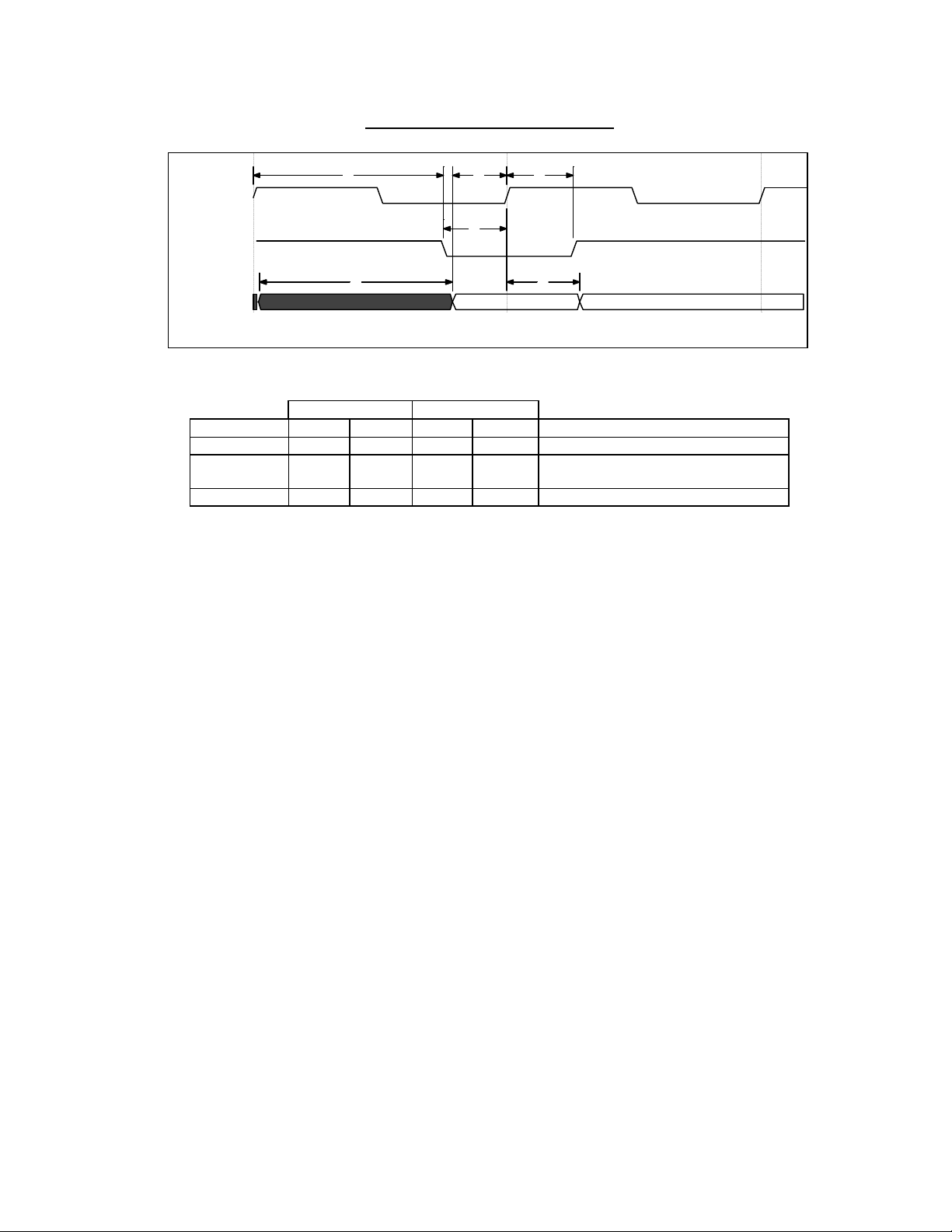
TIMING DIAGRAMS
All Timings are estimated at this time
CBCLK
t2t1t3
t1
nCFRAME
t3t3 t2
nCBE
FIGURE 6 - CardBus COMMAND TIMING
MASTER TARGET
NAME MIN MAX MIN MAX DESCRIPTION
t1 7ns Input setup to clock
t2 2ns 11ns 0ns (Master) Clock to signal valid delay
t3 2ns 11ns Clock to signal valid delay
PCI_CBE.TD
(Target) Input hold time from clock
71
Page 72
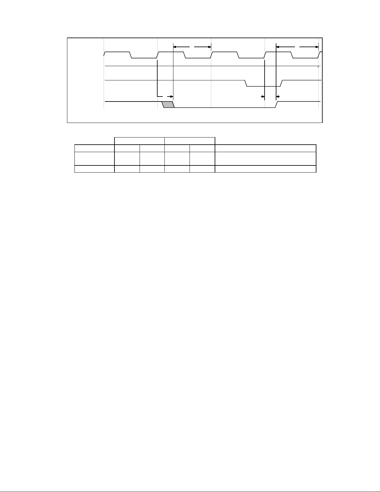
CBCLK
nCFRAME
nCTRDY
nCDEVSEL
FIGURE 7 - CardBus/nCDEVSEL TIMING
MASTER TARGET
NAME MIN MAX MIN MAX DESCRIPTION
t1 0ns 2ns 11ns (Master) Input hold time from clock
(Target) Clock to signal valid delay
t2 7ns Input setup to clock
t2t2
t1t1
PCI_DVSL.TD
72
Page 73
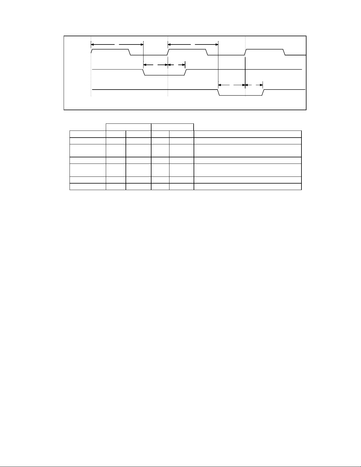
CBCLK
t6t5
t1
t2
nCIRDY
nCTRDY
FIGURE 8 - CardBus/nCIRDY AND nCTRDY TIMING
MASTER TARGET
NAME MIN MAX MIN MAX DESCRIPTION
t1 7ns Input setup time to clock
t2 2ns 11ns 0ns (Master) Clock to signal valid delay
(Target) Input hold time from clock
t3 7ns Input setup time to clock
t4 0ns 2ns 11ns (Master) Input hold time from clock
(Target) Clock to signal valid delay
t5 2ns 11ns Clock to signal valid delay
t6 2ns 11ns Clock to signal valid delay
t3
t4
PCI_IRTR.TD
73
Page 74
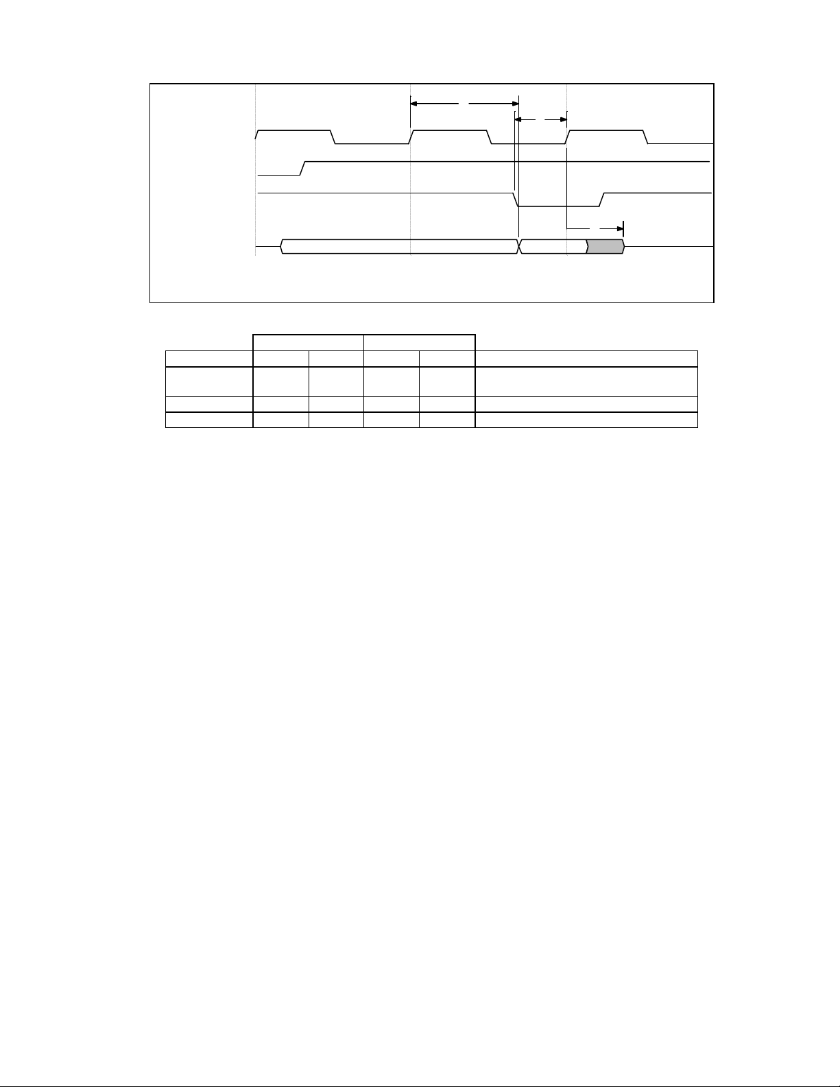
CBCLK
nCFRAME
nCTRDY
t3
t2
CAD (Add/Data)
FIGURE 9 - CardBus/DATA READ TIMING
MASTER TARGET
NAME MIN MAX MIN MAX DESCRIPTION
t1 0ns 2ns 11ns (Master) Input hold time from clock
t2 7ns Input setup time to clock
t3 2ns 11ns Clock to signal valid
t1
PCI_RD.TD
(Target) Clock to signal valid
74
Page 75
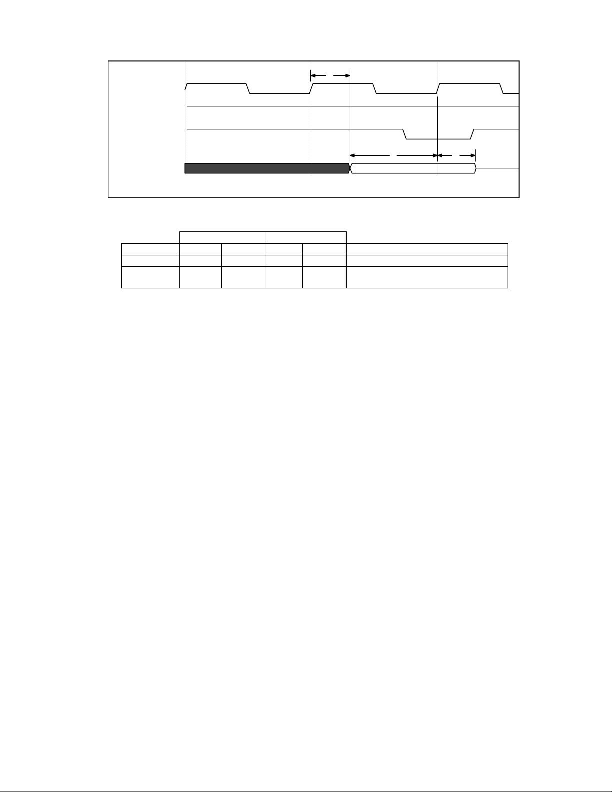
CBCLK
nCFRAME
nCTRDY
t2
CAD (Add/Data)
FIGURE 10 - CardBus/DATA WRITE TIMING
MASTER TARGET
NAME MIN MAX MIN MAX DESCRIPTION
t1 7ns Input setup time to clock
t2 2ns 11ns 0ns (Master) Clock to signal valid delay
(Target) Input hold time from clock
t1
t2
PCI_WR.TD
75
Page 76
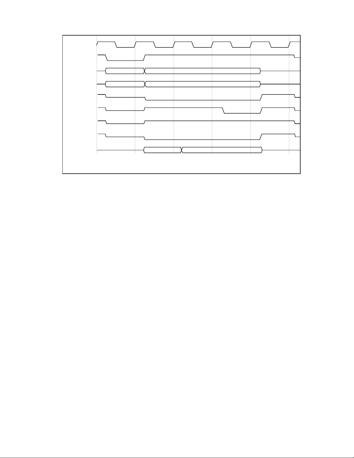
CBCLK
nCFRAME
CAD
nCBE
nCIRDY
nCTRDY
nCSTOP
nCDEVSEL
CPAR
Config Addr
Config Write BE
Addr Par
Config Data
Data Par
TRG_CFWR.TD
FIGURE 11 - CardBus - TYPICAL CONFIGURATION WRITE/EPIC/C IS TARGET
CardBus Bus Cycle Illustration
76
Page 77
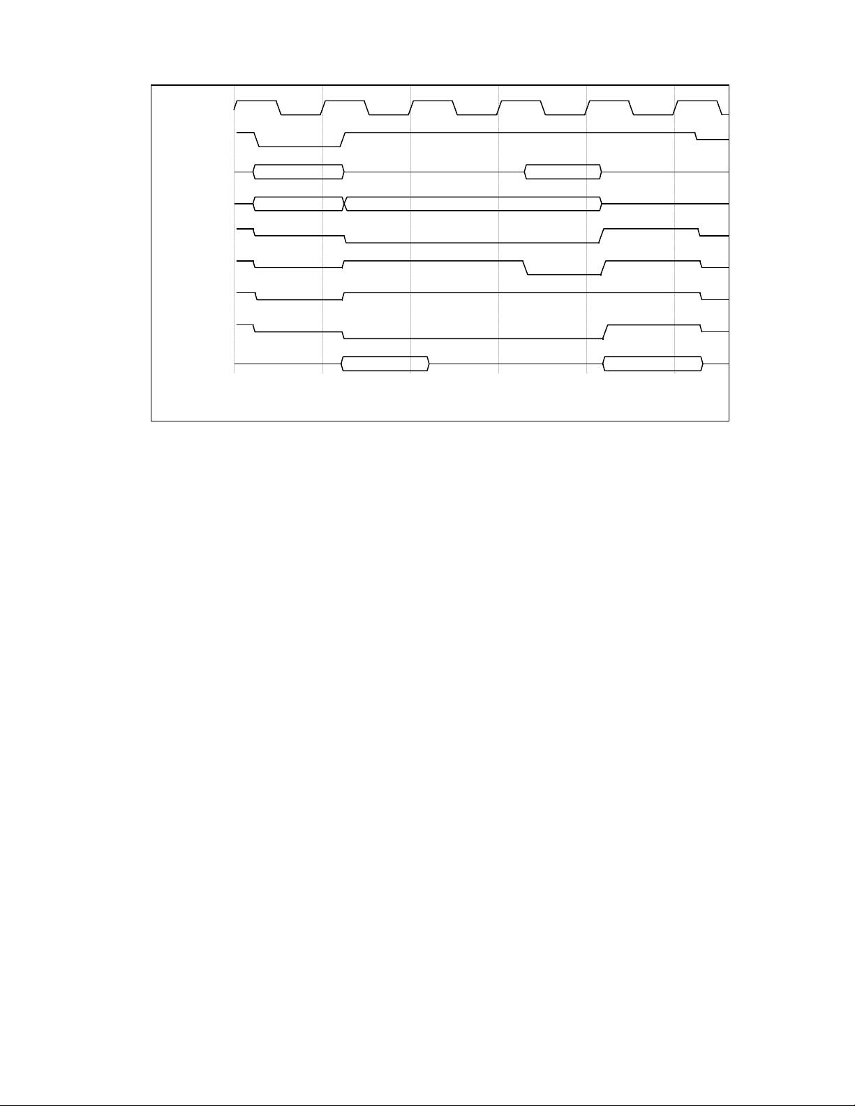
Config Addr
Config Data
Config Read
BE
Addr Par
Data Par
TRG_CFRD.TD
CBCLK
nCFRAME
CAD
nCBE
nCIRDY
nCTRDY
nCSTOP
nCDEVSEL
CPAR
FIGURE 12 - CardBus - TYPICAL CONFIGURATION READ/EPIC/C IS TARGET
CardBus Bus Cycle Illustration
77
Page 78
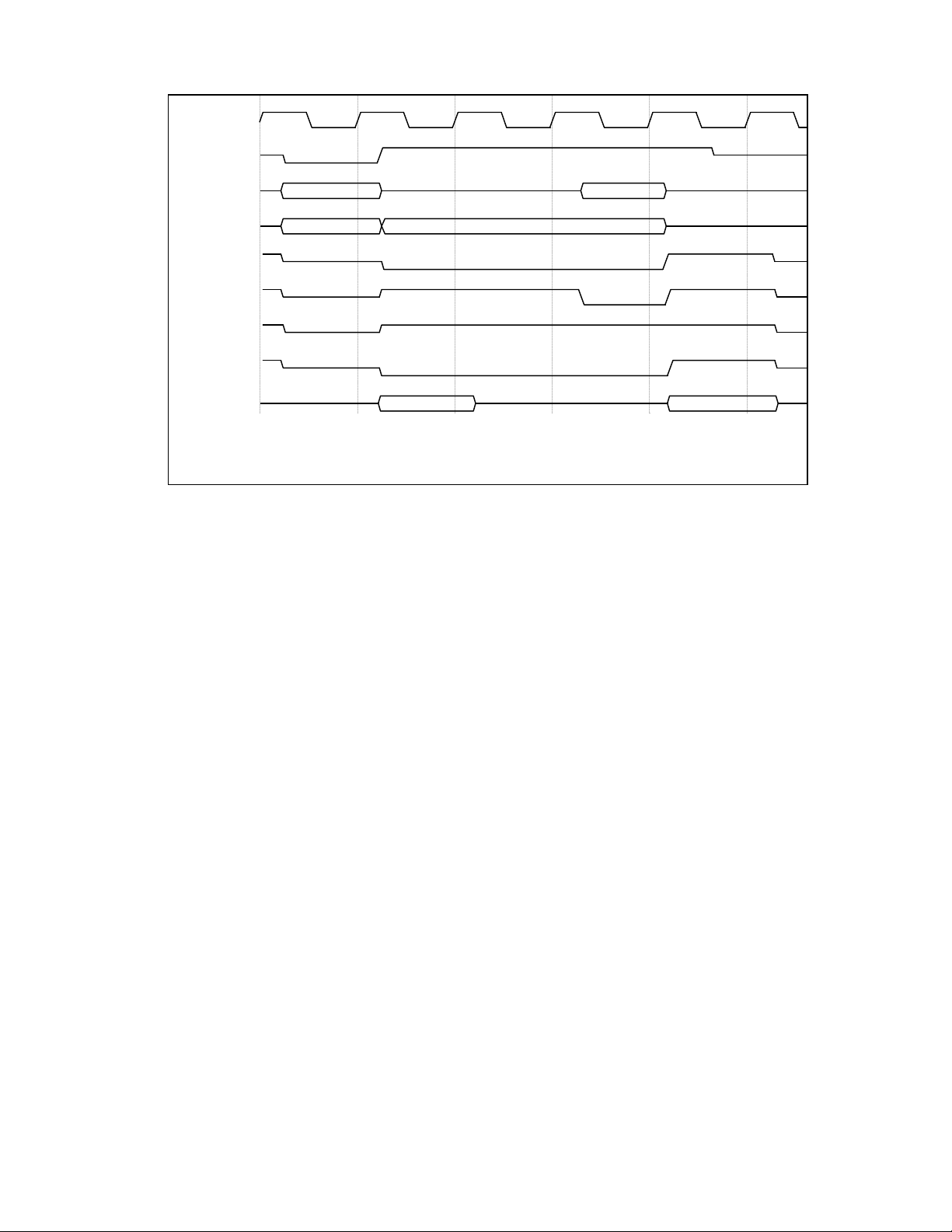
CBCLK
nCFRAME
CAD
nCBE
nCIRDY
nCTRDY
nCSTOP
nCDEVSEL
CPAR
Address Data
I/O Read BE
Addr Par Data Par
TRG_IORD.TD
FIGURE 13 - CardBus - TYPICAL I/O READ/EPIC/C IS TARGET
CardBus Bus Cycle Illustration
78
Page 79
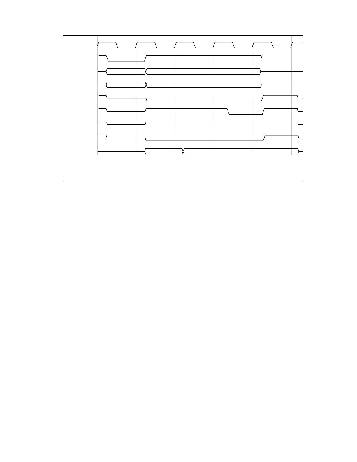
CBCLK
nCFRAME
CAD
nCBE
nCIRDY
nCTRDY
nCSTOP
nCDEVSEL
CPAR
Address
I/O Write BE
Addr Par
Data
Data Par
TRG_IOWR.TD
FIGURE 14 - CardBus - TYPICAL I/O WRITE/EPIC/C IS TARGET
CardBus Bus Cycle Illustration
79
Page 80
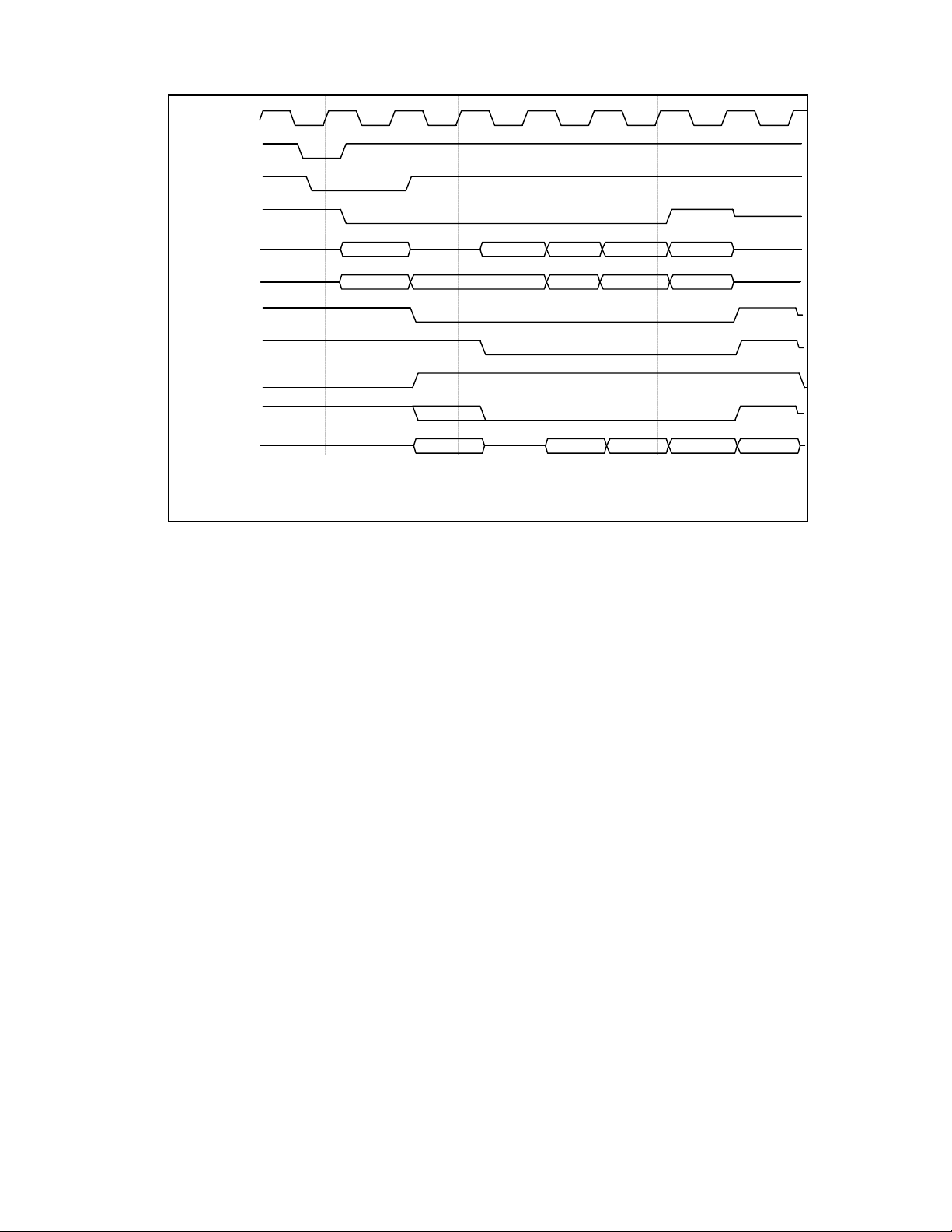
CBCLK
nCREQ
nCGNT
nCFRAME
CAD
nCBE
nCIRDY
nCTRDY
nCSTOP
nCDEVSEL
CPAR
Address Data 1
Read Cmd BE 1
Addr Par Data Par 1
Data 2 Data N
BE NBE 2
Data Par 2 Data Par N
M_RD_S~C.TD
FIGURE 15 - CardBus - TYPICAL READ TRANSACTION/SYSTEM MEMORY TO CHIP
EPIC/C IS BUS MASTER
CardBus Bus Cycle Illustration
80
Page 81

CBCLK
nCREQ
nCGNT
nCFRAME
CAD
nCBE
nCIRDY
nCTRDY
nCSTOP
nCDEVSEL
CPAR
Address Data 1
Write Cmd BE 1
Addr Par Data Par 1
Data 2 Data N
BE 2 BE N
Data Par 2 Data Par N
M_WR_C~S.TD
FIGURE 16 - CardBus - TYPICAL WRITE TRANSACTION/CHIP TO SYSTEM MEMORY
EPIC/C IS BUS MASTER
CardBus Bus Cycle Illustration
81
Page 82
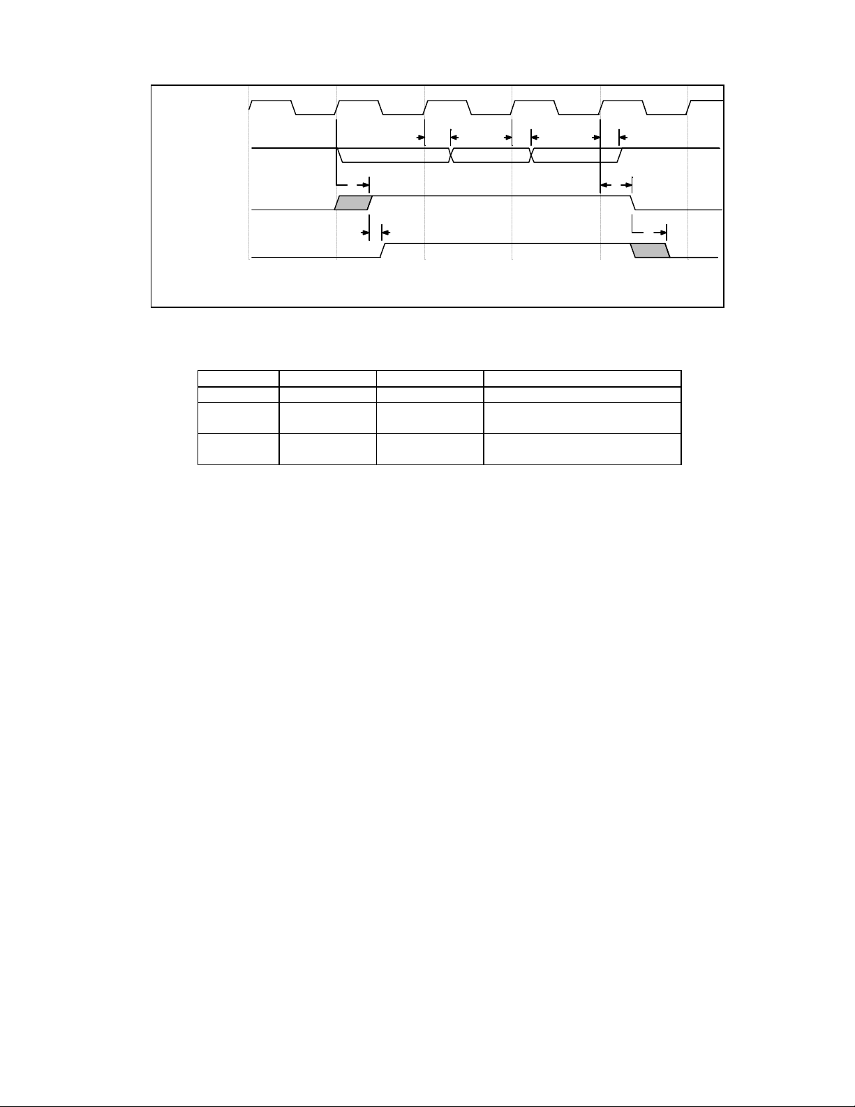
t1t1t1t2t3t1t4
nibble 1
nibble x
last nibble
MII_TX.TD
TX_CLK
TXD
TX_EN
FIGURE 17 - MII - TRANSMIT TIMING FOR 10/100Mb/s
Note: Clock Frequency Changes to 2.5 MHz for 10 Mb/s Nibble Transfers
NAME MIN MAX DESCRIPTION
t1, t2 0ns 25ns Clock to output delay
t3 0ns(100Mb/s)
0ns(10Mb/s)
t4 0ns(100Mb/s)
0ns(10Mb/s)
40ns(100Mb/s)
400ns(10Mb/s)
160ns(100Mb/s)
1.6µs(10Mb/s)
Min: 0 bit times
Max: 4 bit times
Min: 0 bit times
Max: 16 bit times
82
Page 83
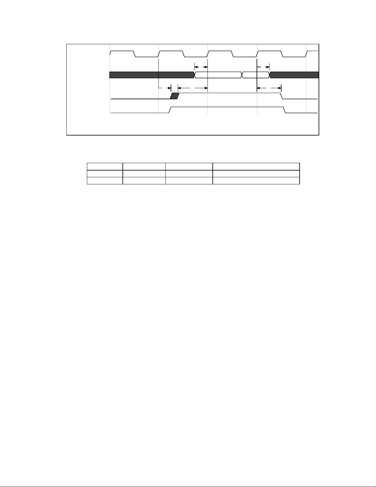
RX_CLK
RXD
RX_DV
CRS (1/2 Dup)
Note: Clock Frequency Changes to 2.5MHz for 10Mb/s Nibble Transfers
NAME MIN MAX DESCRIPTION
t1, t3 10ns Input Setup Time
t2, t4, t5 10ns Input Hold Time
t1
t4
t3
FIGURE 18 - MII - RECEIVE TIMING FOR 100Mb/s
t2
t5
MII_RX1.TD
83
Page 84
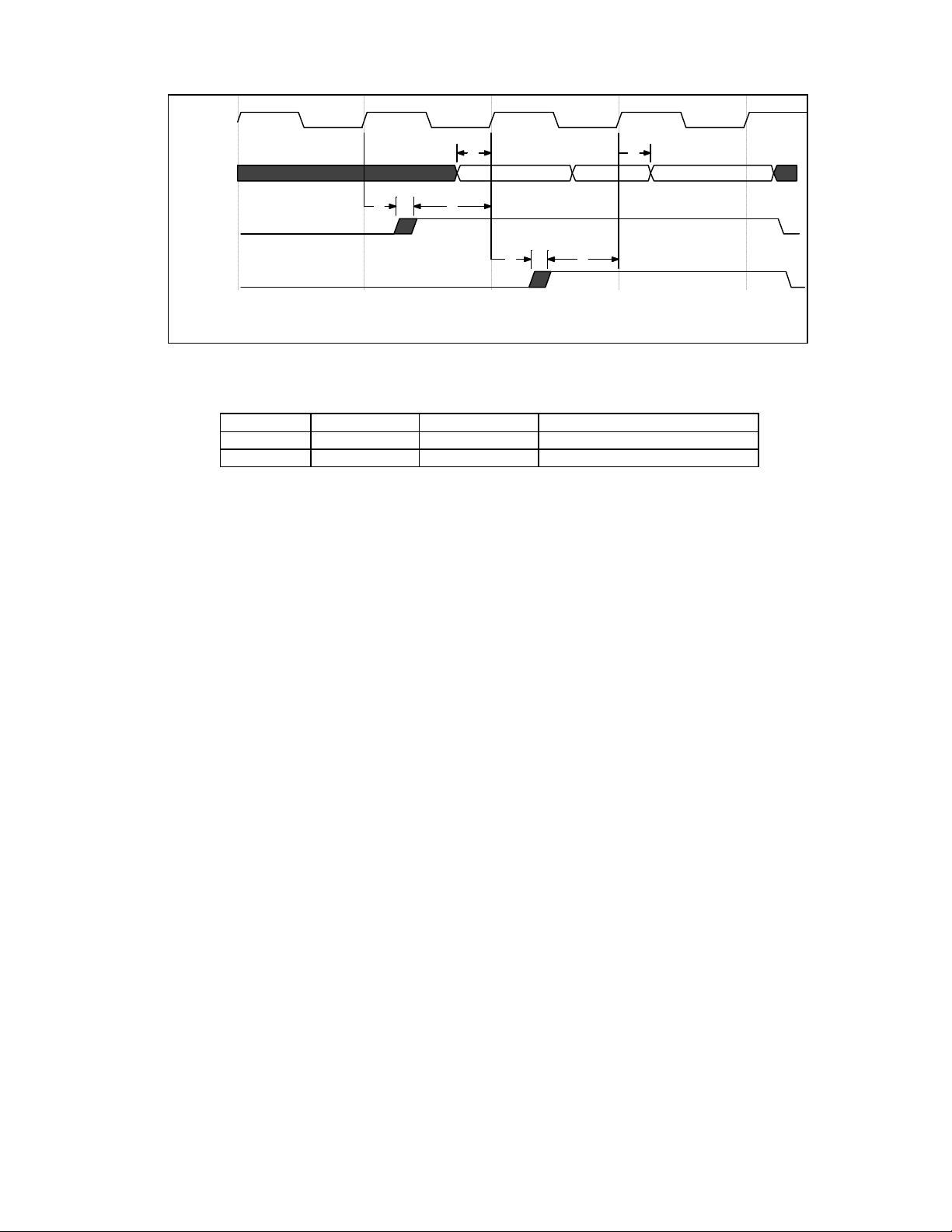
RX_ER expected to be at least 1 clk if CRS (1/2 Dup) error, otherwirse 2 clks
RX_CLK
RXD
RX_DV
RX_ER
t1
t4
t3
t4
t3
t2
MII_RX2.TD
FIGURE 19 - MII - RECEIVE ERROR (RX_ER) TIMING FOR 100Mb/s
Note: Clock Frequency Changes to 2.5 MHz for 10 Mb/s Nibble Transfers
NAME MIN MAX DESCRIPTION
t1, t3 10ns Input Setup Time
t2, t4 10ns Input Hold Time
84
Page 85
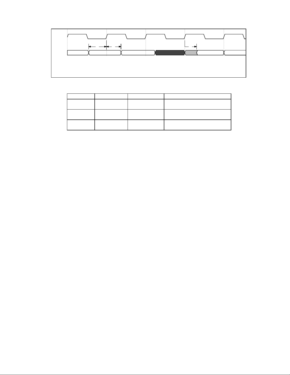
MDC
W R
MDIO
t1 t2 t3
Read DataWrite Data
WRITE READ
MII_MDIO.TD
FIGURE 20 - MII - SERIAL MANAGEMENT WRITE/READ
NAME MIN MAX DESCRIPTION
t1 10ns Data ready before the rising
edge of MCLK (Setup time)
t2 10ns Data hold after the rising edge
of MCLK
t3 0ns 300ns Data ready to MCLK (Required
by EPIC/C)
85
Page 86
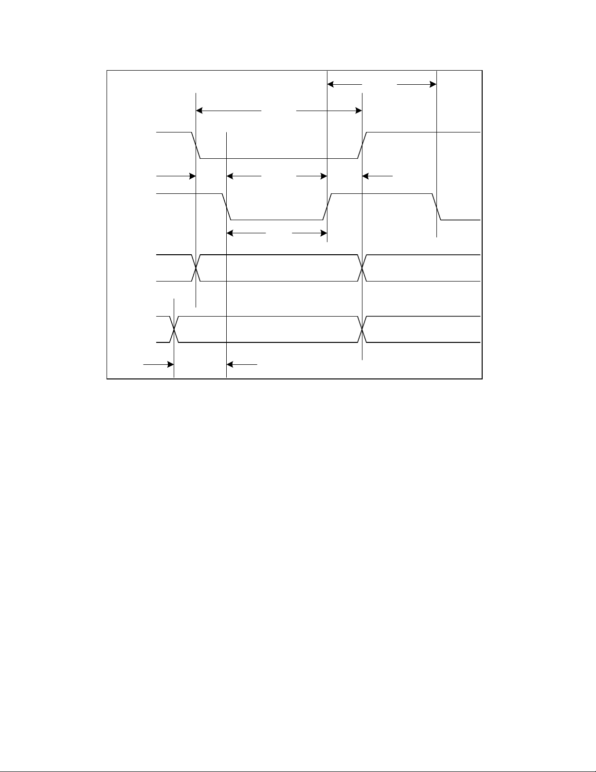
~HCS
t
2
1
t
~HWT
HD(7:0)
HA(x:0)
3
t
5
t
4
t
Valid Data
Valid Address
t
6
FIGURE 21 – MODEM/FLASH RAM WRITE ACCESS
See Table 5 on Page 88
86
Page 87
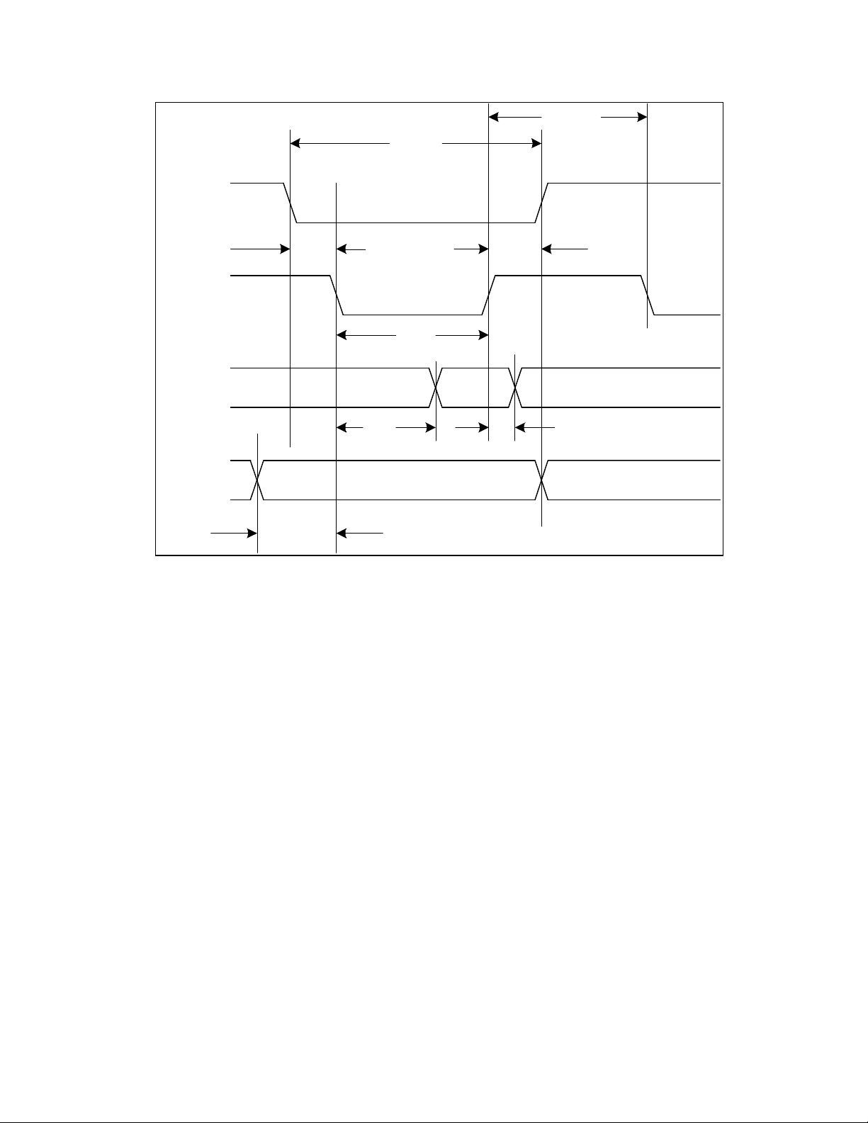
FIGURE 22 - MODEM/FLASH RAM READ ACCESS
Valid Data
~HCS
HA(x:0)
~HRD
HD(7:0)
Valid Address
t
1t2t3t4
t5t6t7t
8
See Table 5 on Page 88
87
Page 88

Table 5 - Modem Access Timings
NAME MIN (NS) MAX (NS) DESCRIPTION
t1 90 Chip select pulse width.
t3 15 Data setup time before write pulse active.
t6 15-45 Address setup time before write or read pulse, optionally
increased for devices requiring longer address setup times.
t5 60 Write pulse width
t4 15 Chip select, data, and address hold time after write pulse
becomes inactive
t7 50-80 Expected data valid on data pins, optionally increased for
devices with slower access times.
t8 0 Data hold time required after read pulse goes inactive.
t2 Selectable Minimum access delay enforced between modem accesses.
Delay determined by preloaded EPIC/C internal register,
NVCTL_m(12:9) from 0 to 15 cbclk periods.
88
Page 89
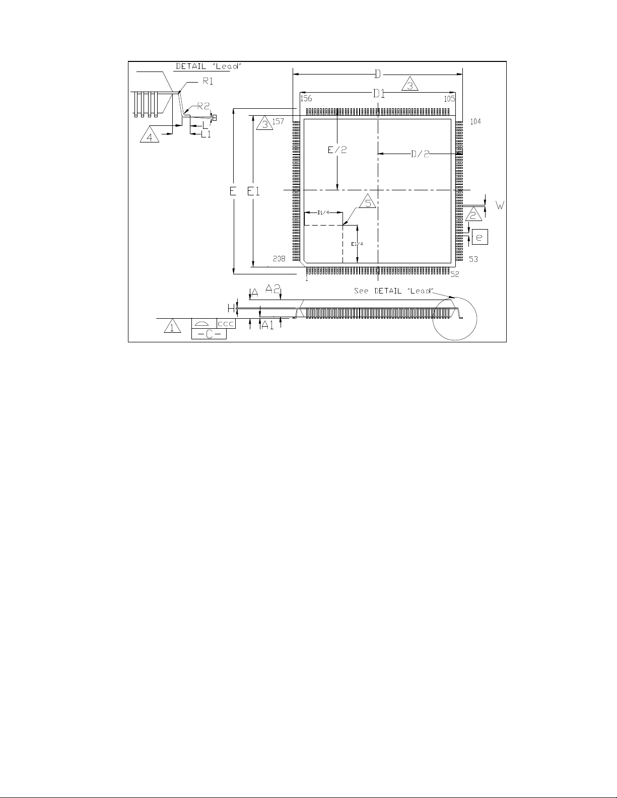
FIGURE 23 - 208 PIN TQFP, 28X28X1.4 BODY, 2 MM FOOTPRINT
See Table 6 on Page 90
89
Page 90

A
1
1
o
o
A1
A2
D
D/2
D1
E
E/2
E1
H
L
L1
e
q
W
R1
R2
ccc
Notes:
1
Controlling Unit: millimeter
2
Tolerance on the position of the leads is ± 0.04 mm maximum
3
Package body dimensions D1 and E1 do not include the mold protrusion. Maximum mold
protrusion is 0.25 mm
4
Dimension for foot length L measured at the gauge plane 0.25 mm above the seating plane is
0.78-1.08 mm
5
Details of pin 1 identifier are optional but must be located within the zone indicated
Table 6 - Package Dimensions
MIN NOMINAL MAX REMARK
~ ~ 1.60 Overall Package Height
0.05 ~ 0.15 Standoff
1.35 ~ 1.45 Body Thickness
29.80 30.00 30.20 X Span
14.90 15.00 15.10
27.90 28.00 28.10 X body Size
29.80 30.00 30.20 Y Span
14.90 15.00 15.10
27.90 28.00 28.10 Y body Size
0.09 ~ 0.23 Lead Frame Thickness
0.45 0.60 0.75 Lead Foot Length from Centerline
~ 1.00 ~ Lead Length
0.50 Basic Lead Pitch
0
~ 7
0.17 ~ 0.27 Lead Width
0.08 ~ ~ Lead Shoulder Radius
0.08 ~ 0.20 Lead Foot Radius
~ ~ 0.08 Coplanarity
/2 X Span Measure from Centerline
/2 Y Span Measure from Centerline
Lead Foot Angle
90
Page 91

91
Page 92

©1997 STANDARD MICROSYSTEMS
CORP.
Circuit diagrams utilizing SMSC products are included as a means of illustrating
typical applications; consequently complete information sufficient for construction
purposes is not necessarily given. The information has been carefully checked and
is believed to be entirely reliable. However, no responsibility is assumed for
inaccuracies. Furthermore, such information does not convey to the purchaser of the
semiconductor devices described any licenses under the patent rights of SMSC or
others. SMSC reserves the right to make changes at any time in order to improve
design and supply the best product possible. SMSC products are not designed,
intended, authorized or warranted for use in any life support or other application
where product failure could cause or contribute to personal injury or severe property
damage. Any and all such uses without prior written approval of an Officer of SMSC
and further testing and/or modification will be fully at the risk of the customer.
LAN83C175 Rev. 07/07/97
 Loading...