

Page 1
MITSUMI
IC for Headphone Stereos LAG673
IC for Headphone Stereos
Monolithic IC LAG673
Outline
This IC was developed for use in 3 V headphone stereos. It incorporates dual preamp, power amp, electronic
volume and motor control circuits; because it requires extremely few external components, it can be used in a
simple circuit configuration.
Features
1. Broad operating voltage range of 2.0 to 5.0 V
2. Few external components required
3. Well-balanced electronic VR, A-curve attenuation characteristic obtained with B-curve VR
4. Internal motor control circuit, with noise from motor driving unit suppressed
5. Fast forward possible using the forced-on pin
Package
SOP-28B (LAG673F)
SDIP-30A (LAG673D)
Absolute Maximum Ratings
Item Symbol Ratings Units
Operating temperature T
OPR
-
20~+65
°
C
Storage temperature T
STG
-
40~+125
°
C
Power supply current V
CC
-
0.3~+7.5 V
Operating voltage Vop 2.0~5.0 V
Power consumption Pd
450 (SOP-28B)
mW
750 (SDIP-30A)
Page 2
MITSUMI
IC for Headphone Stereos LAG673
Electrical Characteristics
(Except where noted otherwise, Ta=25°C)
Item Symbol Measurement conditions Min. Typ. Max. Units
Consumption current
I
CC VIN=0V, IM=0mA 18 25 mA
(excluding motor speed controller unit)
Preamp unit (Ta=25°C)
Open-circuit gain Gvo Vo=
-
10dBm, RL=∞ 72 dB
Closed-circuit gain Gvc Vo=
-
10dBm 40 42 44 dB
Maximum output voltage Vom THD=10% 0.30 0.45 Vrms
Total harmonic distortion ratio THD V
OUT=400mVrms 0.05 0.5 %
Output noise voltage Vno
V
IN
=0V, Rg=2.2kΩ, BPF=30Hz~20kHz
150 300
µVrms
Input impedance Zin VOUT=
-
10dBm 18 22 kΩ
Crosstalk between channels C · T Rg=2.2kΩ, V
OUT=
-
10dBm 30 dB
Output voltage with preamp off Vooff V
IN=100mVrms
-
50 dB
Output resistance with preamp off Rooff 10 kΩ
Input resistance with preamp off Rioff 10 kΩ
Attenuator unit (Ta=25
°
C)
Maximum input voltage Vi max. 0.2 Vrms
Maximum attenuation Va max. Vcont=min. 66 dB
Attenuation error Vaerr Vcont=max. 0 dB
Input impedance Zia 15 20 kΩ
Control pin input resistance Zicot 100 kΩ
Power amp unit (Ta=25
°
C)
Voltage gain Gv P
OUT=5mW 26 28 30 dB
Voltage gain difference between channels
Gv Vcont=max. 0 3 dB
Maximum output power I Pom THD=10%, R
L=32Ω 20 28 mW
Maximum output power II Pom THD=10%, R
L=16Ω 30 mW
Total harmonic distortion ratio THD P
OUT=5mW 0.2 2.0 %
Crosstalk between channels C · T P
OUT=5mW 45 55 dB
Output noise voltage Vn Rg=2.2kΩ, Vcont=min. 0.25 1.0
mVrms
Ripple rejection RR 100Hz, 100mVp-p4250dB
Noise of preamp + power amp Vnto V
IN=0V, Rg=2.2kΩ, Vcont=max. 6 9
mVrms
Motor control unit (Ta=25°C)
Consumption current IMC 3.0 5.0 mA
Startup current IMS 500 mA
Reference voltage Vref Between RML
-
ADJ pins 0.72 0.80 0.87 V
Reference voltage fluctuation I Vref1 V
CC between 2.0 and 5.0V
*
0.05 %/V
Reference voltage fluctuation II Vref2 I
M between 25 and 250 mA 0.01
%/mA
Reference voltage fluctuation III Vref3 Ta between -10 and 50°C 0.01 %/°C
Current coefficient K 323843
Current coefficient fluctuation IK1V
CC between 2.0 and 6.5 V 0.5 %/V
Current coefficient fluctuation II K 2 I
M between 25 and 250 mA 0.05
%/mA
Current coefficient fluctuation III K3 Ta between -10 and 60°C 0.02 %/°C
Output voltage on forced on VCEsa T
M=200mA 0.6 V
Input resistance on forced on Rion 5.6 kΩ
Leakage current on forced off IML 200 µA
Input resistance on forced off Ricon 33 kΩ
Conditions: V
CC=3.0 V, IM = 100 mA Motor: M25E-7 (Mitsumi model)
*
Voltage drift between pins 17 and 13
VRL
K=
------------R1 IM
Page 3
MITSUMI
IC for Headphone Stereos LAG673
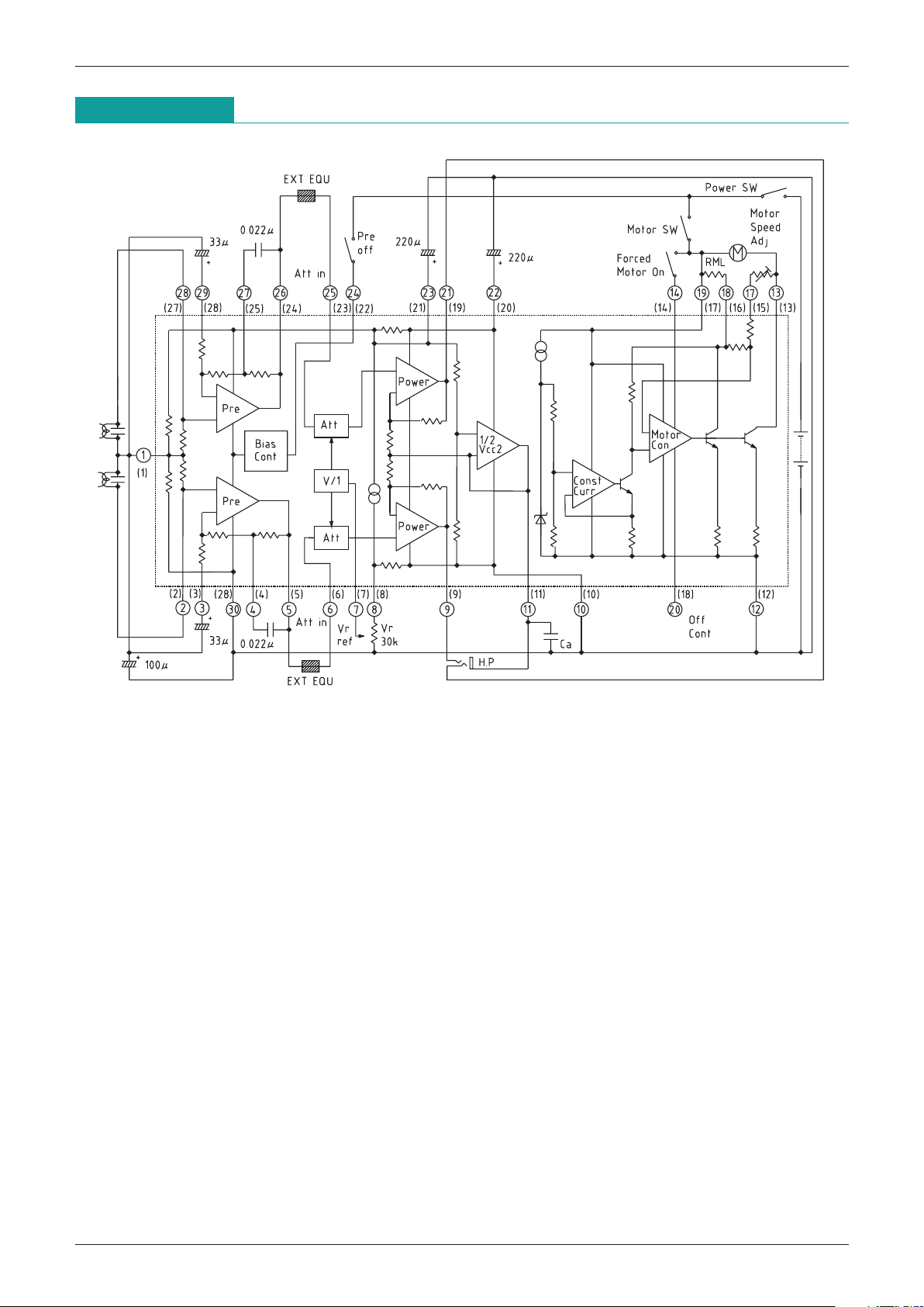
Block Diagram
1: The motor speed potentiometer is 1.5 kΩ (assuming the motor used is Mitsumi M25E-7; if the optimal
adjustment range is not obtained using a different motor, add a fixed resistance).
2: RML = motor load correction resistance
3: Connecting the preamp off pin to +V
CC turns the preamp circuits off.
4: Connecting the motor forced-on pin to +V
CC turns the motor on (no control).
5: in circles are pin numbers for a DIP-30P package; numbers in parentheses ( ) are for an SOP-28B
package.
6: In the DIP-30P package, pins 15 and 16 are NC.
7: Ca is a 100,000 pF capacitor used to prevent oscillation of the 1/2 V
CC amp circuit.
Page 4
MITSUMI
IC for Headphone Stereos LAG673
Characteristics
100
60
50
40
30
20
10
80
70
10 100 1k 10k 100k
Frequency (Hz)
VCC=3.0V
When VR=max.
TOTAL GAIN
POWER AMP GAIN
Gain (dB)
-
10
-
20
-
30
-
40
-
50
1.0 2.0 3.0 4.0 5.00
Ripple rejection (V)
PREAMP OFF
V
R=max.
F
R=100Hz
V
R=100mVrms
R
L=16Ω
Ripple rejection rate-V
CC
Power supply voltage (dB)
-
10
-
20
-
30
-
40
-
50
100 1k 10k 100k
Frequency (Hz)
VCC=3.0V
Crosstalk frequency
Crosstalk (dB)
40
50
60
70
30
20
10
Power supply voltage (V)
1.0 2.0 3.0 4.0 5.00
5
10
15
20
I
CC-VCC
RL=16Ω
R
L=32Ω
I
OC (RL=16Ω)
Power supply output
(THD=10%) P
OUT max. (mW)
No-load consumption current (mA)
100
10
1
0.1
0.1 1 10 100
Power supply output (mW)
VCC=1.8V
V
CC=2.0V
V
CC=3.0V
THD-POUT
Total harmonic
distortion ratio (%)
THD-VOUT
10.0
1.0
0.1
0.01
-
30
-
20
-
10 0
Output voltage (dBm)
VCC=1.8V
V
CC=2.0V
V
CC=3.0V
Total harmonic distortion ratio (%)
0
-
20
-
40
-
60
-
80
0/6 1/6 2/6 3/6 4/6 5/6 6/6
(min.) (max.)
Voltage controllability
(B curve mechanical volume knob)
VCC=3.0V
V
ATT-VCONT
Output voltage attenuation (dB)
Preamp
Power ampP
OUT.
Power amp
Power amp
Voltage gain vs. Frequency
Attenuator
 Loading...