

Page 1
MITSUMI
IC for Headphone Stereos (bass boost) LAG668
IC for Headphone Stereos (bass boost)
Monolithic IC LAG 668
Outline
This IC was developed to provide bass boost functions without deviating from the basic design concept of
Mitsumi's LAG665, which is highly regarded for applications in headphone stereos for overseas markets in
particular.
Bass boost functions are widely adopted in models for overseas markets as well. However, because of
stringent cost constraints, there has been a need for an IC which is simple and inexpensive. This IC can
provide bass boost functions simply by adding three resistors and one capacitor (per channel).
Moreover, it has the same pinout as the LAG665, so that by making selective use of set features, a product
lineup can be developed without changes to the printed circuit board.
Features
1. Configuration: pre and power amps, motor control, E. VR, bass boost
2. Preamp off function convenient for use in models with radios
3. Independent motor control circuit
1. Motor noise is effectively suppressed
2. With motor on/off pin (motor can be stopped easily when radio is in use)
3. With fast forward pin
4. Bass boost frequency characteristic can be changed simply by changing the resistance multiplier.
5. Well-balanced E. VR circuit
1. L, R channels variable using a single VR
2. A-curve can be reproduced using B-curve VR
6. Few external components
Package
SOP-28B (LAG668F)
SDIP-30A (LAG668D)
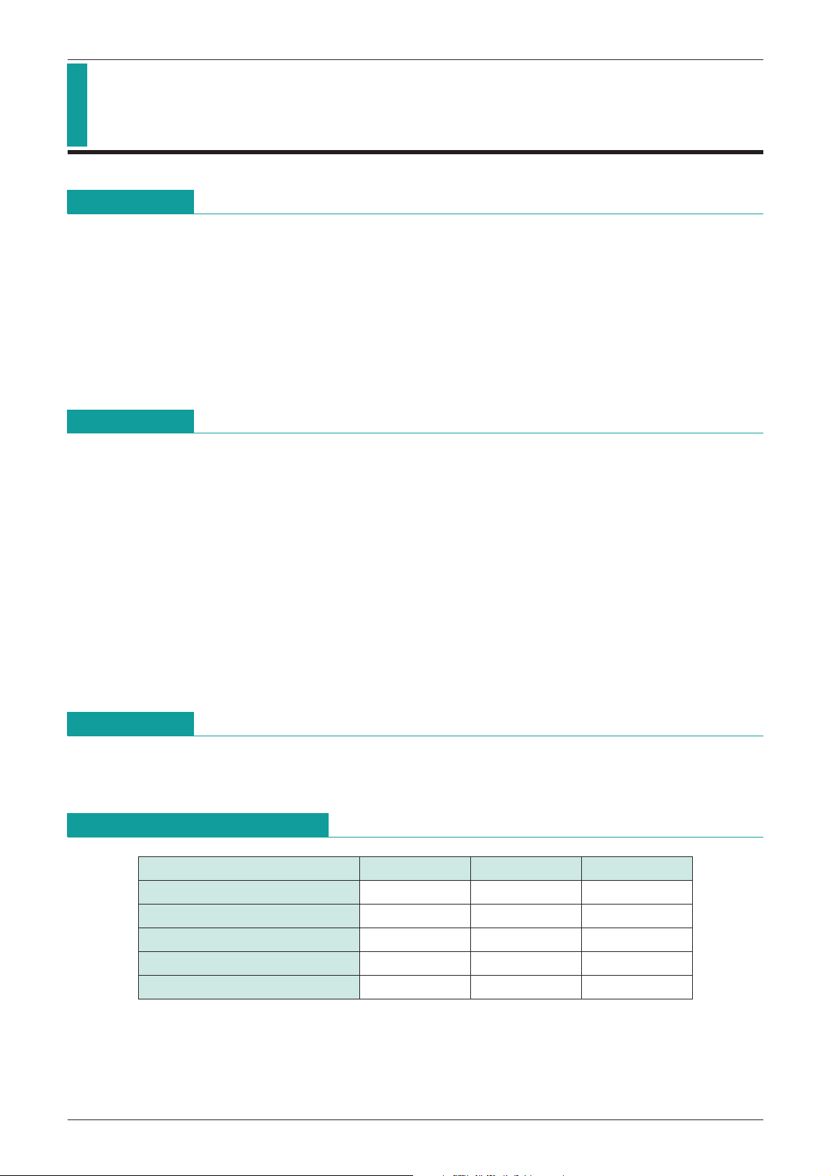
Absolute Maximum Ratings
Item Symbol Ratings Units
Operating temperature T
Storage temperature T
Power supply current V
Power consumption Pd
Operating voltage Vop +2.0~+5.0 V
OPR
STG
CC max.
-
20~+65
-
40~+125
-
0.3~+7.5 V
DIP : 750, SOP : 450
°
C
°
C
mW
Page 2
MITSUMI
IC for Headphone Stereos (bass boost) LAG668
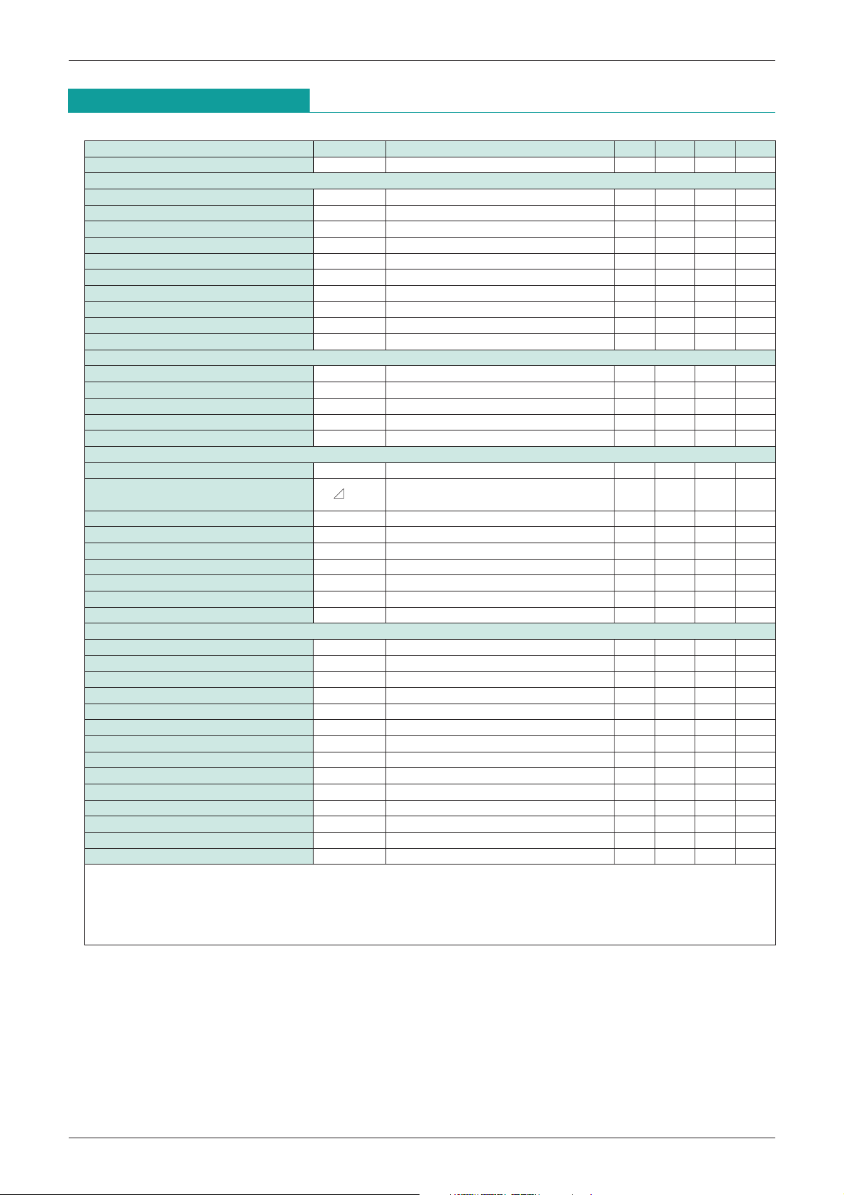
Electrical Characteristics
Item Symbol Measurement conditions
(Except where noted otherwise, Ta=25°C)
Min. Typ. Max. Units
Consumption current ICC VIN=0v, IM=0mA 18 25 mA
Preamp unit (Ta=25
Open-circuit gain Gvo V
Closed-circuit gain Gvc V
°
C)
O=
-
10dBm, RL=infinite 72 dB
O=
-
10dBm 40 42 44 dB
Maximum output voltage Vom THD=10% 0.45 0.6 Vrms
Total harmonic distortion ratio THD V
Output noise voltage Vno V
IN=0, Rg=2.2k, BPF (30~20kHz) 150 300
Input impedance ZIN VOUT=
Crosstalk between channels C.T Rg=2.2k, V
Output voltage with pre off Vooff V
OUT=400mVrms 0.05 0.5 %
-
10dBm 18 22 kΩ
OUT=
-
10dBm 30 dB
IN=100mVrms
-
50 dB
Output resistance with pre off Rooff 10 kΩ
Input resistance on pre off Rioff 10 kΩ
°
Attenuator unit (Ta=25
C)
Maximum input voltage Vi max. 0.2 Vrms
Maximum attenuation Va max. Vcont=min. 66 dB
Attenuation error Vaerr Vcont=max. 0 dB
Input impedance Z
IN 200 kΩ
Control pin input resistance Zicot 100 kΩ
Power amp unit (Ta=25
Voltage gain Gv P
Voltage gain difference
between channels
Maximum output power I Pom1 THD=10%, R
Maximum output power II Pom2 THD=10%, R
Total harmonic distortion ratio THD P
Crosstalk between channels C.T P
°
C)
OUT=5mW 36 38 40 dB
Gv Vcont=max. 0 3 dB
L=32Ω 20 28 mW
L=16Ω 30 mW
OUT=5mW 0.5 2.0 %
OUT=5mW 20 30 dB
Output noise voltage Vn Rg=2.2k, Vcont=max. 1.0 2.0
Ripple rejection RR VCC=3V, 100Hz, 100mVp-p3137 dB
Noise of preamp + power amp + B.B.
Vnto VIN=0, Rg=2.2k, Vcont=max. *1 3.0 6.0
Motor control unit (Ta=25°C)
Consumption current IMC 3.0 5.0 mA
Startup current IMS 500 mA
Reference voltage Vref Between RML
Reference voltage fluctuation I Vref1 V
Reference voltage fluctuation II Vref2 I
CC between 2.1 and 5.0 V 0.05 %/V
M between 25 and 250 mA 0.01
-
ADJ pins 0.72 0.80 0.87 V
Reference voltage fluctuation III Vref3 Ta between -10 and 50°C 0.01 %/°C
Current coefficient K 323843
Current coefficient fluctuation IK1 V
Current coefficient fluctuation II K 2 I
CC between 2.1 and 5.0 V 0.5 %/V
M between 25 and 250 mA 0.05
Current coefficient fluctuation III K3 Ta between -10 and 50°C 0.02 %/°C
Output voltage on forced on VCEsa I
M=200mA, 14PIN=VCC 0.6 V
Input resistance on forced on Rion 5.6 kΩ
Leakage current on forced off IML 200 µA
Input resistance on forced off Ricon 33 kΩ
Conditions unless stated otherwise
*
Amp unit: V
Motor unit: V
CC=3.0V, f=1kHz, RL=16Ω, Pre OFF=OPEN
CC=3.0V, IM=100mA, Motor unit: (Mitsumi model)
Note 1: Bass boost circuit constants are based on application circuit diagrams.
Note 2: Motor pin voltage fluctuations
µVrms
mVrms
mVrms
%/mA
%/mA
Page 3
MITSUMI
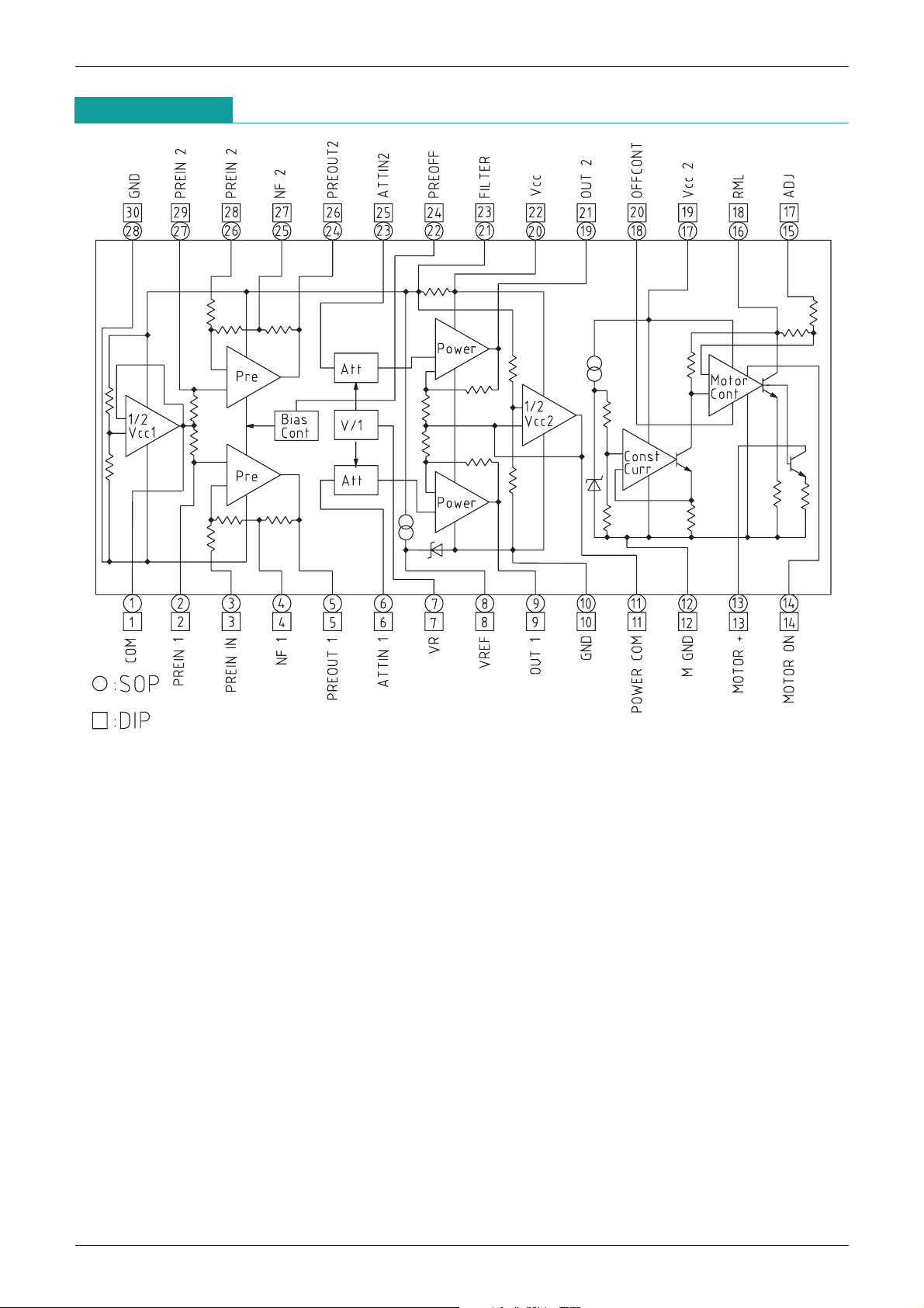
Block Diagram
IC for Headphone Stereos (bass boost) LAG668
Page 4
MITSUMI
GV
GVH
GVL
B•B Off
B
•
B ON
40
35
30
25
15
10
1
10
2
10
3
10
4
10
5
10
6
Frequency (Hz)
f1 f2
3dB
3dB
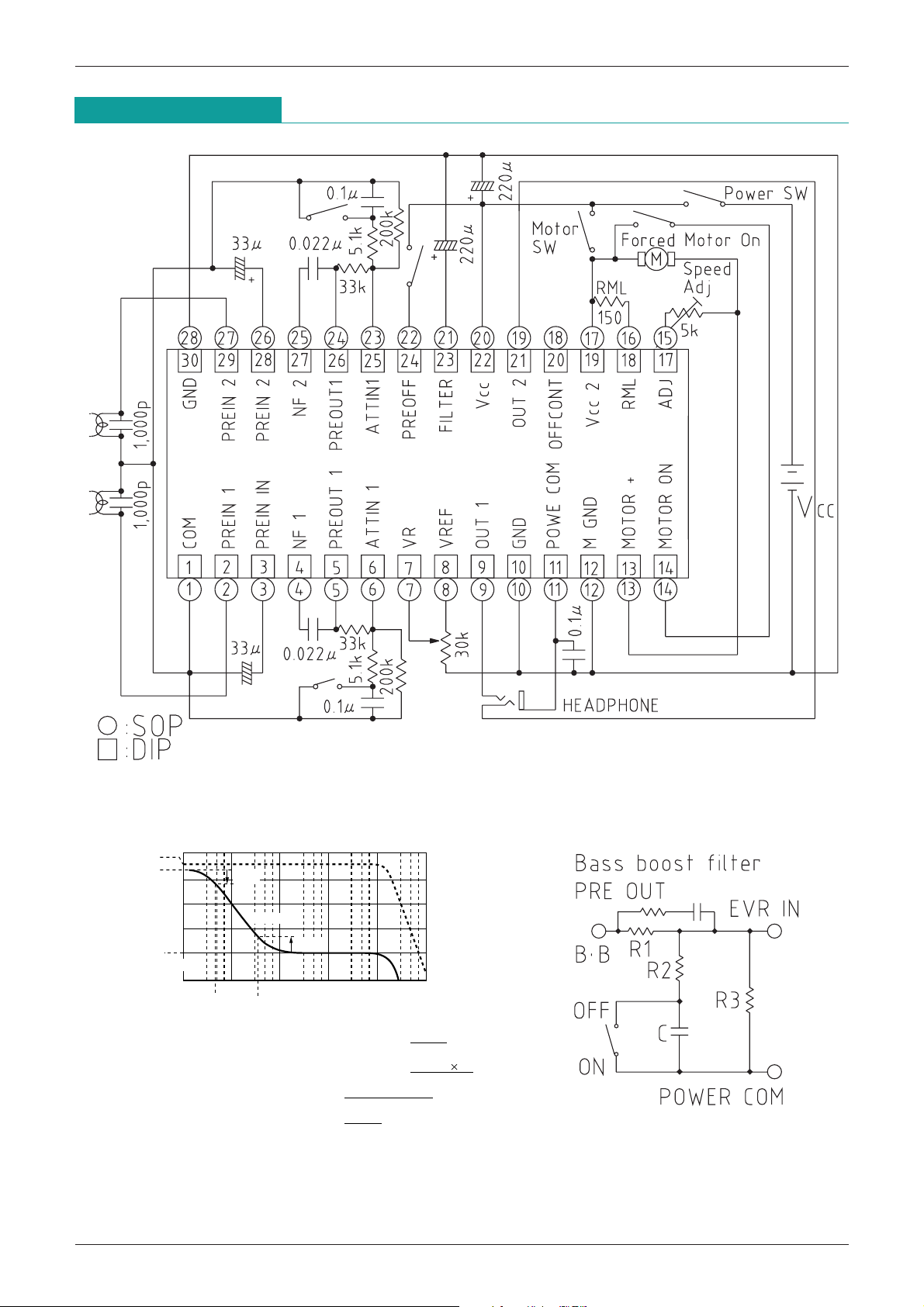
GV : Power amp gain GVH=GV+20Log (dB)
f1, f2: Cutoff frequencies
G
VH : Bass boost power amp gain
(high level)
G
VL : Bass boost power amp gain
(low level, or boost off)
(
(
R1+R3
R3
GVL=GV+20Log (dB)
(
(
R2//R3+ R1
R2//R3
R1
f1= (Hz)
2π ((R
1//R3) +R2)C
1
f2= (Hz)
2πR
2C
1
Power amp gain
(dB)
Application Circuits
IC for Headphone Stereos (bass boost) LAG668
Bass Boost Power Amp Gain
Page 5
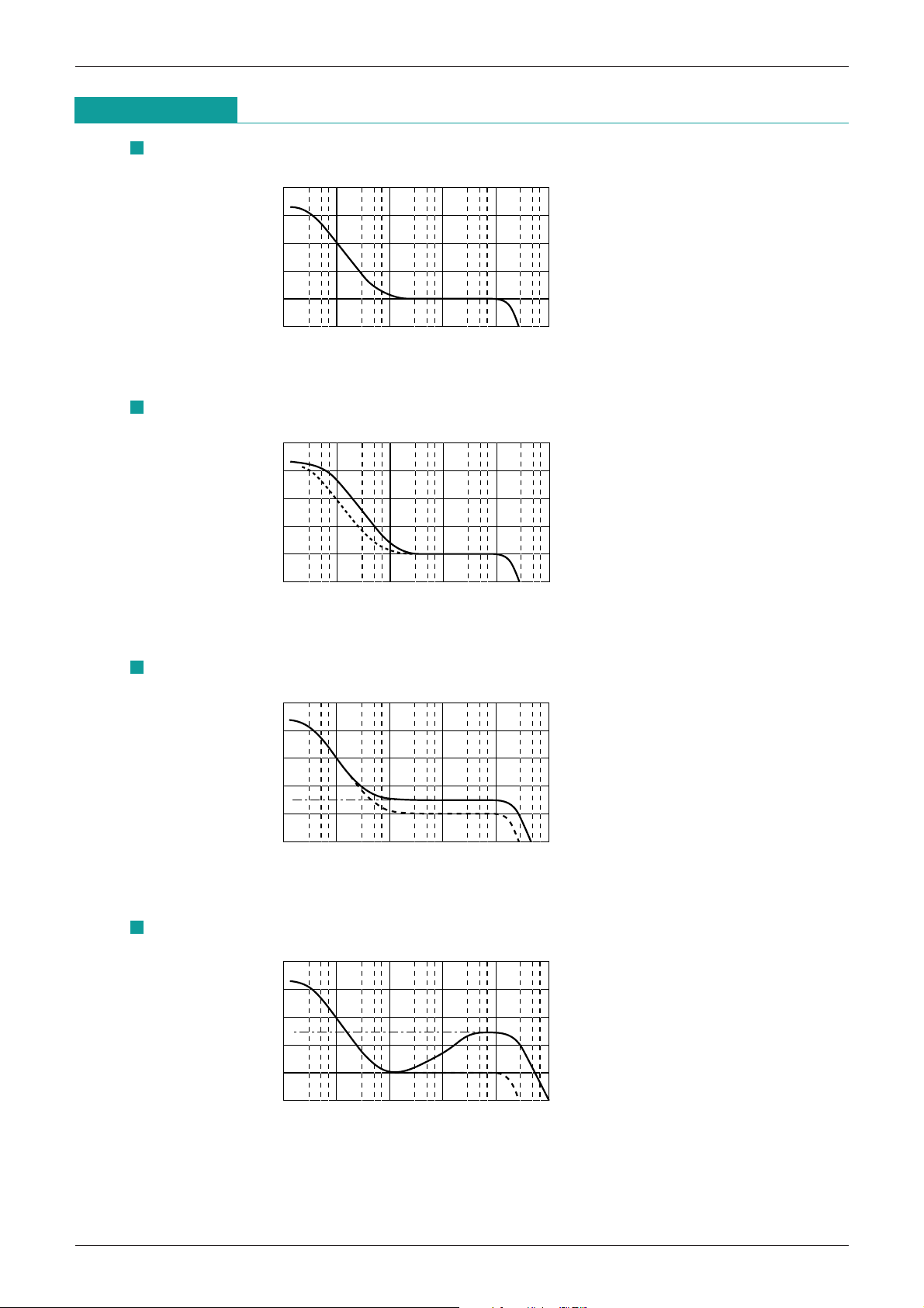
MITSUMI
40
35
30
25
20
15
10
1
10
2
10
3
10
4
10
5
10
6
Frequency (Hz)
R1=33kΩ
R2=6.8kΩ
R3=180kΩ
C=0.1µF
GVH=37dB
G
VL=23dB
f1=50Hz
f2=230Hz
No R4 or C2
Power amp gain (dB)
R1=33kΩ
R2=4.7kΩ
R4=20kΩ
R3=180kΩ
C=0.1µF
C2=390pF
GVH=37dB
G
VH=27dB
G
VL=20dB
f1=50Hz
f2=340Hz
40
35
30
25
20
15
10
1
10
2
10
3
10
4
10
5
10
6
Frequency (Hz)
Power amp gain (dB)
40
35
30
25
20
15
10
1
10
2
10
3
10
4
10
5
10
6
Frequency (Hz)
R1=33kΩ
R2=4.7kΩ
R3=180kΩ
C=0.1µF
GVH=37dB
G
VL=20dB
f1=50Hz
f2=340Hz
No R4 or C2
Power amp gain (dB)
40
35
30
25
20
15
10
1
10
2
10
3
10
4
10
5
10
6
Frequency (Hz)
R1=12kΩ
R2=2.2kΩ
R3=180kΩ
C=0.1µF
GVH=37dB
G
VL=20dB
f1=130Hz
f2=720Hz
No R4 or C2
Power amp gain (dB)
IC for Headphone Stereos (bass boost) LAG668
Characteristics
Recommended constants
Bass boost efficiency
(Bass boost)
Response for poor headphone and cassette head characteristics
Bass + treble boost
 Loading...