

Page 1
MITSUMI
IC for Multifunction Telephones LAG640
IC for Multifunction Telephones
Monolithic IC LAG640
This IC was developed for use in multifunctional telephones with security features; it has the following
functions.
Features
1. Incorporates efficient switching regulator with broad input voltage range
V
OUT 5V±0.25 IL 250mA (13~45V)
V
IN 15~45V
2. Internal data transmission/reception circuits
Data can be superposed on the power supply line for transmission.
Can be switched between two different input modes
3. Internal system reset circuit
5V line abnormal voltage detection circuit
Watchdog timer reset circuit
4. Internal speaker amp
260 mW typ. at 8Ω load
Mute pin
5. Internal beep sound generator circuit
With pin to vary audio volume (also used to turn beep sound on and off)
Package
SDIP-30A (LAG640D)
Absolute Maximum Ratings
(Ta=25°C)
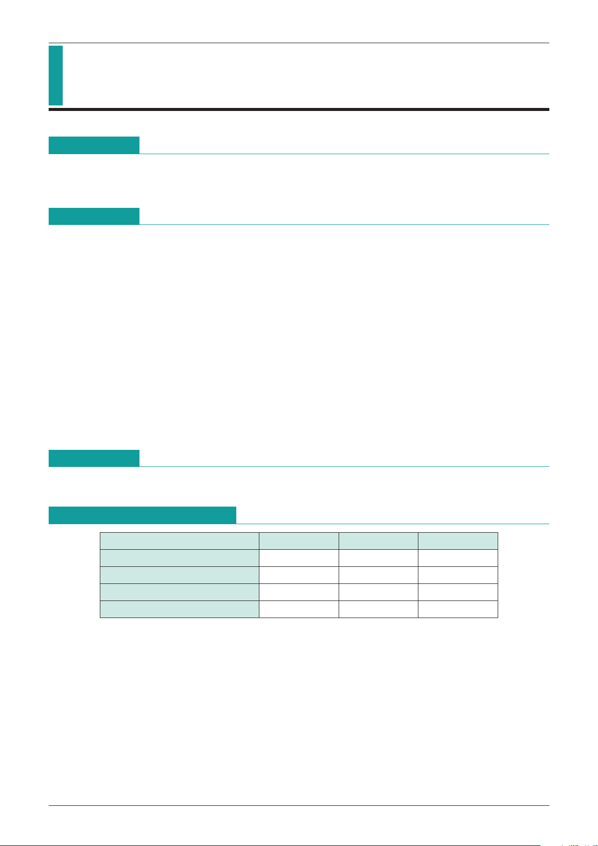
Item Symbol Ratings Units
Operating temperature T
OPR
-
20~+70
°
C
Storage temperature T
STG
-
40~+125
°
C
Power supply current V
CC max. 46 V
Allowable loss Pd 750 mW
Outline
Page 2
MITSUMI
IC for Multifunction Telephones LAG640
Electrical Characteristics
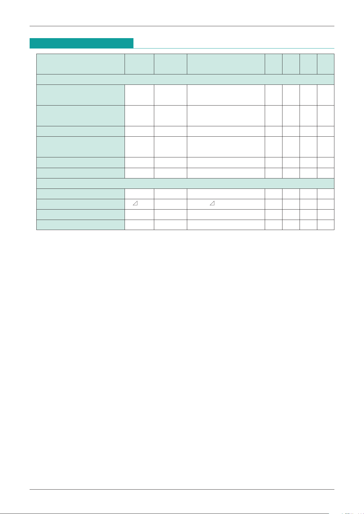
(Except where noted otherwise, Ta=25°C, VCC=30V)
Item Symbol
Measurement
Measurement conditions Min. Typ. Max. Units
circuit
SWR unit
Output voltage (5V) V
O11
V
CC=15~45V
4.75 5.00 5.25 V
I
L=0~250mA
Output voltage (5V) V
O21
V
CC=13~45V
4.70 5.00 5.25 V
I
L=0~200mA
Output ripple voltage Vr 1 I
L=250mA 50
mV
P-P
Reactive current ICCq1
I
L=0mA
610mA
Amp & Transmission unit
SWR oscillation frequency F
OSC 180kHz
Output current on short-circuit I
OS 1RS=0.2Ω 70 110 150 mA
Power supply voltage detection unit
Detection voltage V
S 2
*
4.30 4.50 4.80 V
Detection drop voltage V
S 2VS=Vo
-
VS 0.2 V
Output current while on IR
ON 2 Vo=4V 10 20
mA
Leakage output current while off
IROFF 2 Vo=5.25V 1 µA
Note: The asterisk (*) indicates that the power supply voltage detection unit characteristics are standards in
the transient power on/off states. However, for convenience the detection voltage is taken to be the
value of V
0 when V0 in measurement circuit 2 is varied and the pin 6 output state is switched from off
to on.
Page 3
MITSUMI
IC for Multifunction Telephones LAG640
Electrical Characteristics
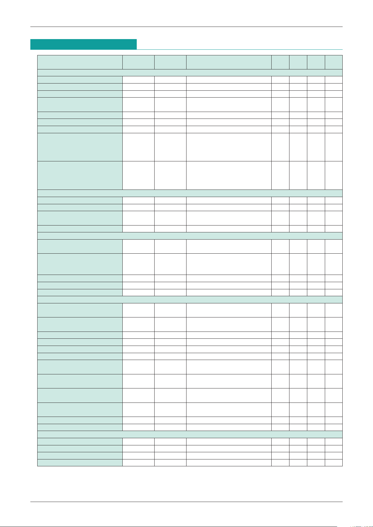
(Except where noted otherwise, Ta=25°C, VCC=30V Faudio=1kHz)
Item Symbol
Measurement
Measurement conditions
Min. Typ. Max. Units
circuit
Power amp unit
Amp gain G
V 1 Voa=0.775Vrms 37 40 43 dB
Maximum distortion-free output
PO max. 1 THD=10% 150 260 mV
Distortion THD 1 P
O=100mW 5 %
Attenuation at 100 Hz GF1/GF0 1
F
O=1kHz, Fl=100Hz
-
14 dB
Voa=0.775Vrms
Attenuation at 10 Hz GF2/GF0 1 F2=10 kHz, above conditions
-
8dB
Input IMP 1 R
IN1 3 Mute off 10 15 kΩ
Input IMP 2 R
IN2 3 Mute on 2.5 3.5 kΩ
Mute on
Residual noise 1 Vno1 1
AUDIO IN 20mVrms
0.5
mVrms
IL=10 70mA 1.5kHz
Transmission unit on Ft=1kHz
Mute off
Residual noise 2 Vno2 1
AUDIO OFF
1.2
mVrms
IL=10 70mA 1.5kHz
Transmission unit on Ft=1kHz
Beep sound generator unit
Beep sound frequency Fb 1 0.85 1.0 1.15 kHz
Beep off switching point Ibsw 1 Pin 9 input current 20 35 48 µA
Beep sound output 1 Vob1 1
Pin 9 connected to GND through 4.7k
1.0 1.4 1.8 Vrms
Amp output voltage
Beep sound output 2 Vob2 1
Pin 9 connected to GND through 47k
0.11 0.16 0.22 Vrms
Watchdog timer unit
Timer time Tt 1
cf. watchdog timer
2.4 3.0 3.6 S
waveform diagram
cf. watchdog timer
0.45 1.1
Output pulse width T
PW 1 waveform diagram mS
T=beep sound period
(1/2T)
(1T)
Output voltage while on Vw
ON 1 0.5 V
Leakage output current while off
IwOFF 11µA
Timer-clearing pulse width Tcl 1 5 µS
Transmission circuit unit
Transmission output voltage (1)
Vto1 2
R
L-110Ω, peak value
5.1 5.8 6.6
Vp-p
across pins L3-L4
Transmission output voltage (2)
Vto2 2
R
L-1Ω, peak value
5.5 6.2 7.0
Vp-p
across pins L3-L4
L3 pin voltage VL3 2 No signal 4.0 4.4 4.8 V
L4 pin voltage VL4 2 No signal 0.5 0.7 0.9 V
Reception sensitivity Vrs 2 0.8 1.0 1.2
Vp-p
Input IMP RIN3 4 Both pins 7and 8 14 20 26 kΩ
Transmission delay time Td1 2
cf. transmit/receive
0.4 µS
waveform diagrams
Transmission delay time Td2 2
cf. transmit/receive
0.4 µS
waveform diagrams
Transmission delay time Td3 2
cf. transmit/receive
0.8 µS
waveform diagrams
Transmission delay time Td4 2
cf. transmit/receive
0.8 µS
waveform diagrams
Reception output H voltage VroH 2 R
L=10kΩ 4.5 V
Reception output L voltage VroL 2 R
L=1.5kΩ 0.5 V
General logic unit characteristics
H level input voltage ViH 3 2.4 V
L level input voltage ViL 3 0.8 V
H level input current IiH 3 V
IN=2.4V 10 µA
L level input current IiL 3 V
IN=0.4V
-
300 µA
Page 4
MITSUMI
IC for Multifunction Telephones LAG640
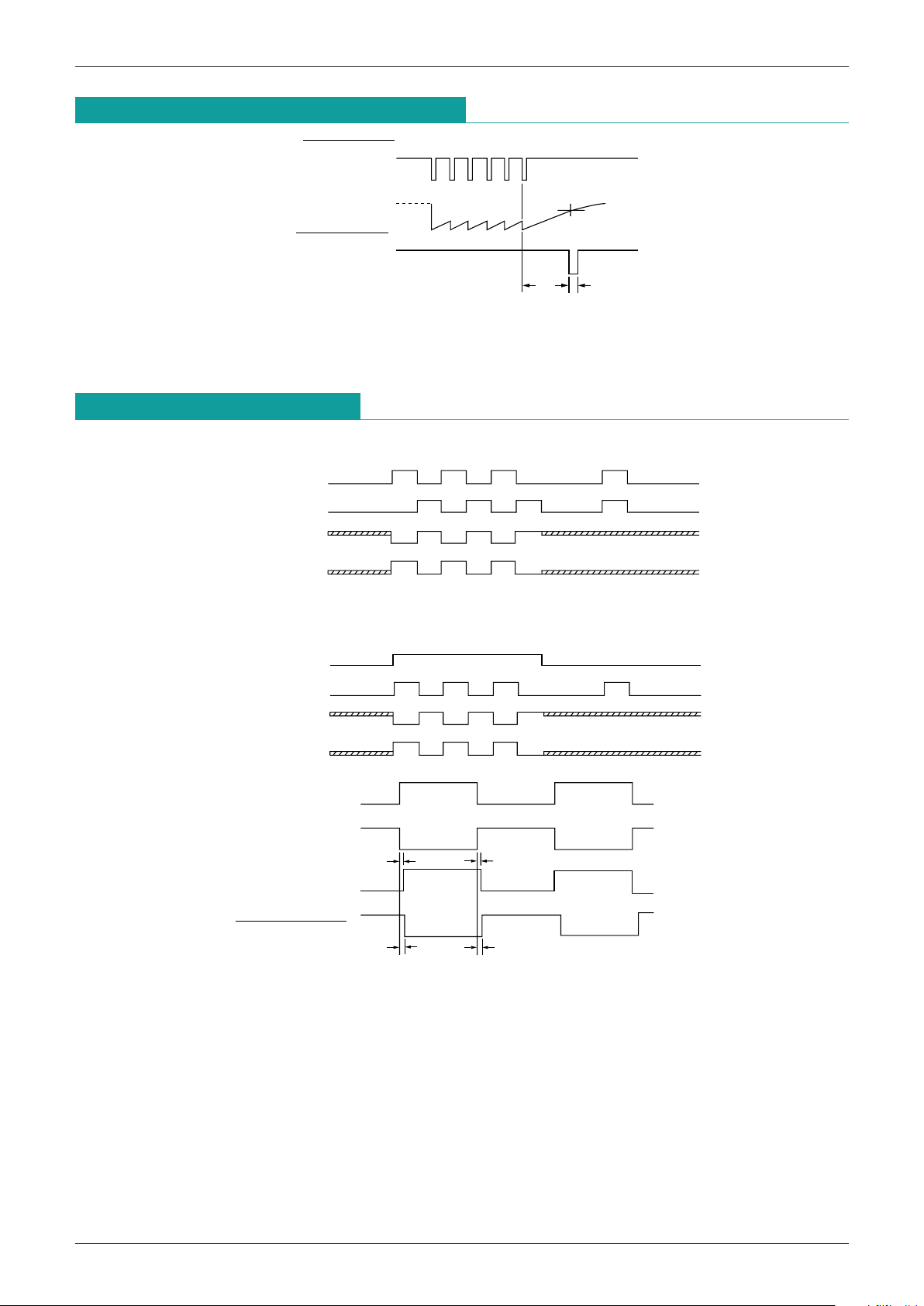
Watchdog Timer Waveform Diagrams
Tt
Tpw
TIMER CLEAR
(22PIN)
(21PIN)
Interrupt output
(20PIN)
Note: Pulses to clear the timer must have
a width of 5µs or more.
Transmit/receive Waveform
1. When pulling pin 25 up to VDD (+5V)
SG (24PIN)
SD (DTC) 23PIN
L3 (27PIN)
L4 (26PIN)
2. When shorting pin 25 to GND
SG (24PIN)
SD (DTC) 23PIN
L3 (27PIN)
L4 (26PIN)
Td2
Td1
Td4
Td3
SG
L3
L4
Reception data out
Page 5
MITSUMI
IC for Multifunction Telephones LAG640
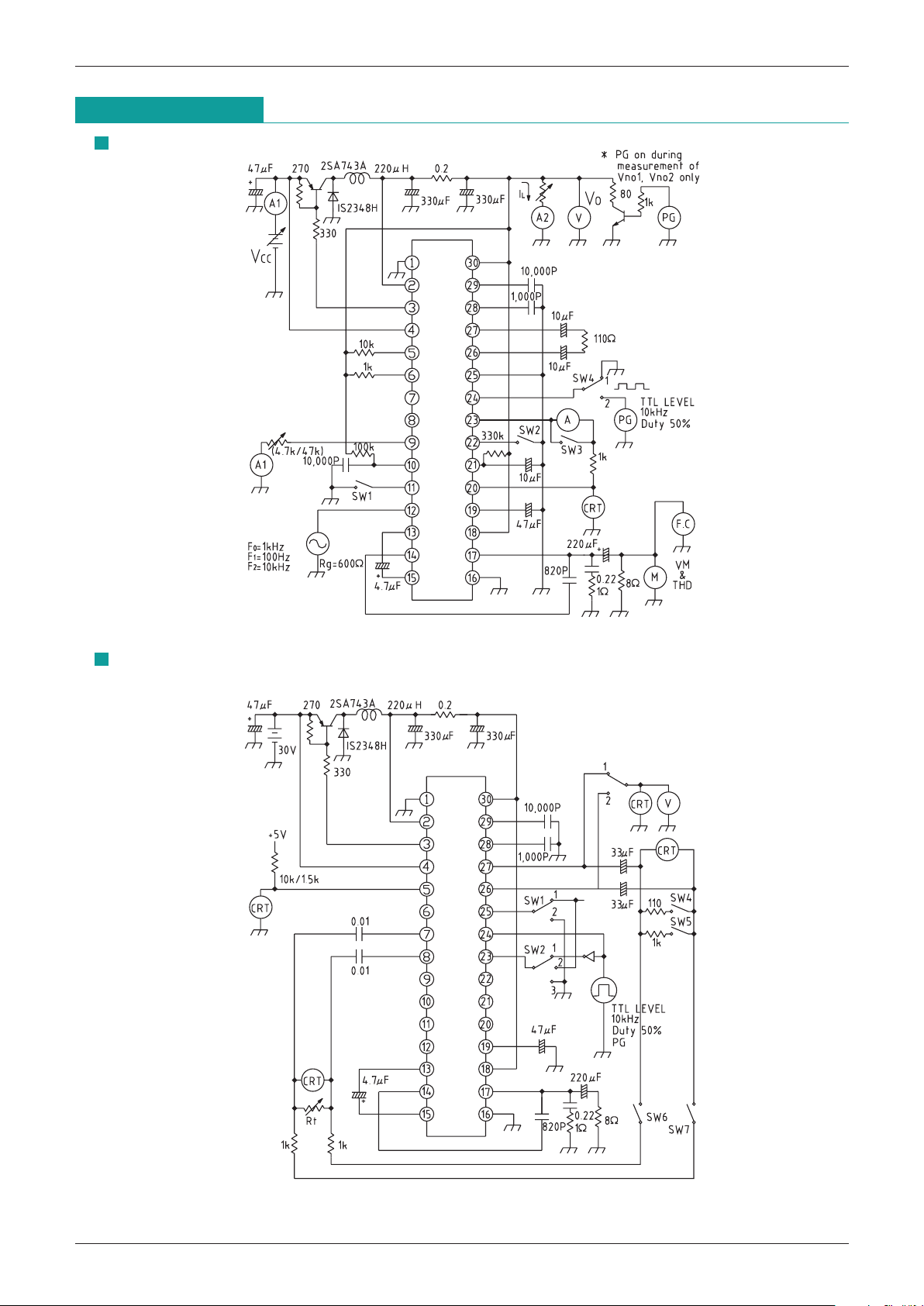
Measuring Circuit
Measurement circuit 1
Measurement circuit 2
Page 6
MITSUMI
IC for Multifunction Telephones LAG640
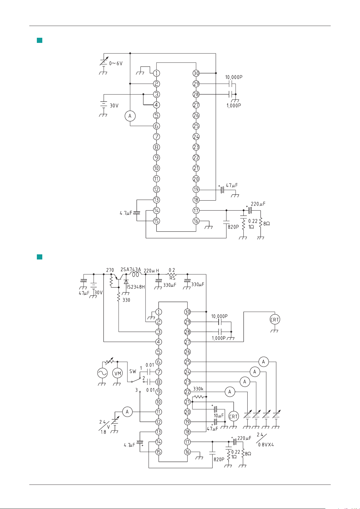
Measurement circuit 3
Measurement circuit 4
Page 7
MITSUMI
IC for Multifunction Telephones LAG640
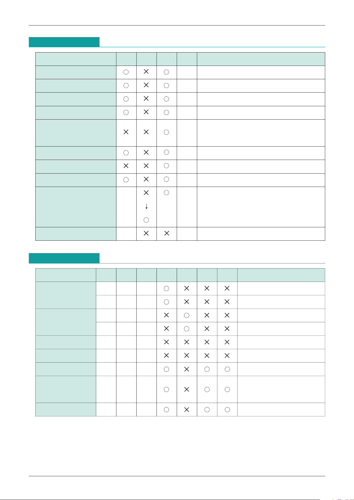
Switch Operation
(Measurement circuit 1)
Measurement item SW1 SW2 SW3 SW4 Other Conditions
Vo1, Vo2 1
Vr 1 No spike noise
I
CCq 1 A1 only
I
OS 1 A2 only
G
V, PO max., THD
1
THD measured after passing through
GF1/GF0, GF2/GF0 400Hz-15kHz BPF
Vno1 2 Using 400Hz-15kHz BPF
Vno2 2 Using 400Hz-15kHz BPF
Fb, IbSW, Vob1, Vob2 1
-
1
Tt, T
PW, Vwon, Tcl cf. watchdog timer waveform diagram
I
WOFF
-
1
Switch Operation
(Measurement circuit 2)
Measurement SW1 SW2 SW3 SW4 SW5 SW6 SW7
Vto1
11
-
Peak value across pins L3, L4
22
-
Peak value across pins L3, L4
Vto2
11
-
Peak value across pins L3, L4
22
-
Peak value across pins L3, L4
VL3 231
VL4 232
Vrs 22
-
Measured with Rt adjusted
Td1~Td4 22
-
cf. transmit/receive
waveform diagrams
VroH, VroL 22
-
Page 8
MITSUMI
IC for Multifunction Telephones LAG640
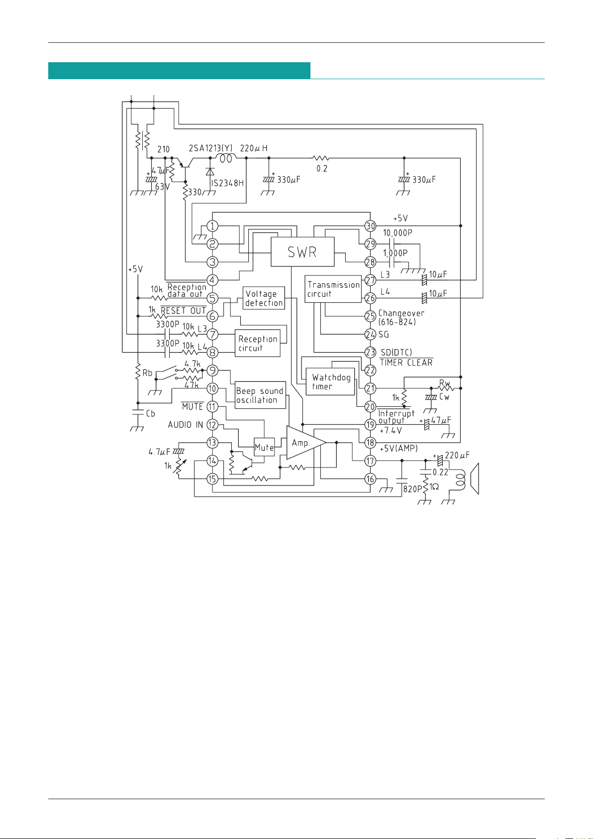
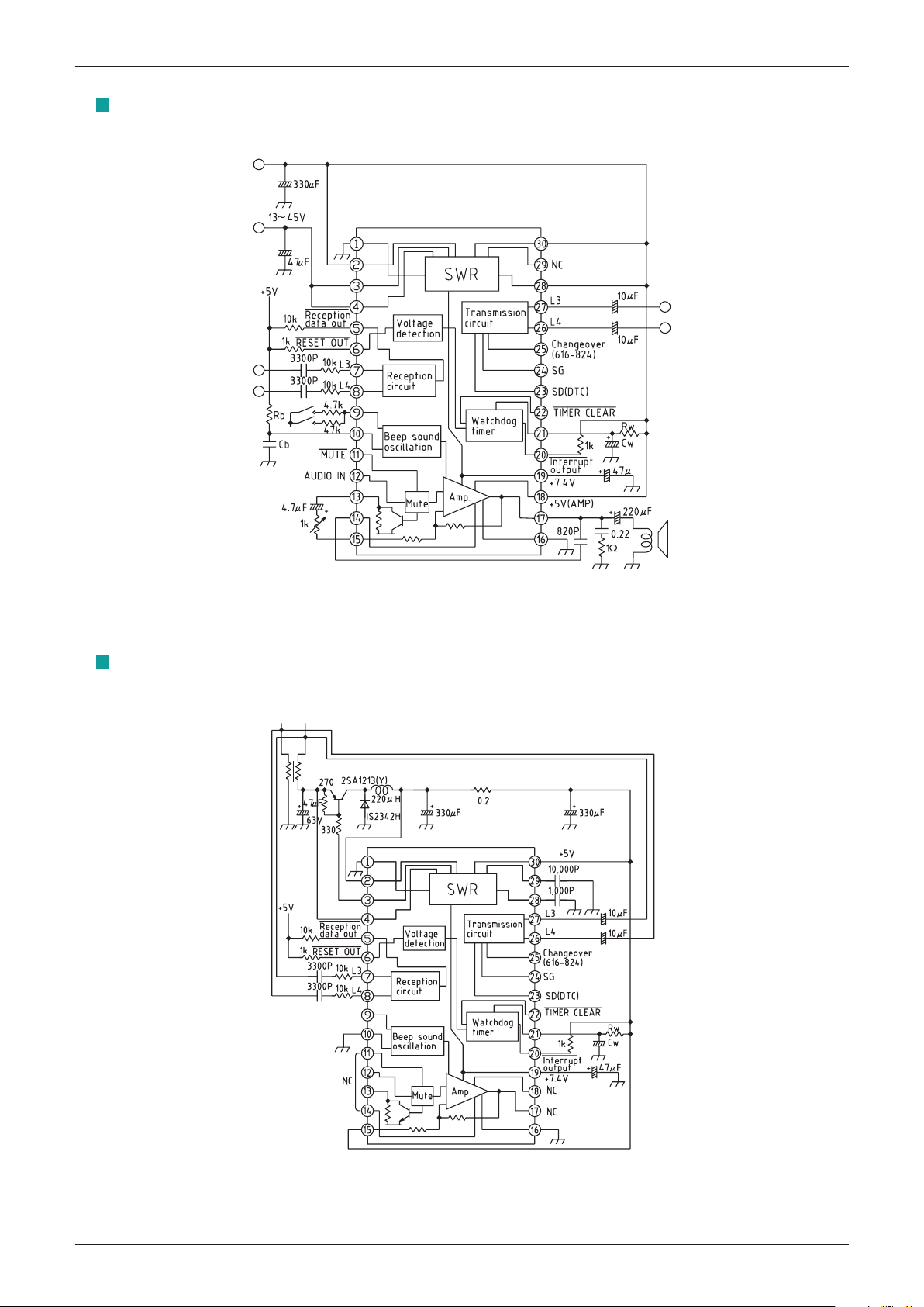
Block Diagram and Application Circuits
1. The watchdog timer time is determined by the values of Rw and Cw.
Tt .=.Rw
· Cw where Rw is 56k to 560kΩ
Cw is between 0.01µF and 10µF
2. The beep sound frequency is determined by Rb and Cb.
Fb .=.1/Rb
· Cb where Rb is 56k to 330kΩ
Cb is between 4700PF and 22,000PF.
3. The beep sound volume can be varied through the resistance connected to pin 10.
4.7kΩ the voltage is approx. 4V
P-P, and at 47kΩ it is about 0.4VP-P.
4. In overload protection operation the voltage across pins 1 to 30 is tested, with a limit of 100 ±20mV.
On load shorting, the test voltage is dropped to about 1/4 to conserve power.
Page 9
MITSUMI
IC for Multifunction Telephones LAG640
Even when a 5V external voltage can be supplied, an addition voltage of 13 to 45V must be applied to
pins 3 and 4 in order to obtain an internal biased power supply of 7.4V.
In order to prevent abnormal oscillation of the amplification circuit, a 5 V power supply must be
connected to pin 15 to halt amplification functions.
(SWR circuit not used)
Additional application example 1
(Speaker amp not used)
Additional application example 2
Page 10
MITSUMI
IC for Multifunction Telephones LAG640
Notes on Use
1. Protection from high-frequency noise
In consideration of applications in which telephone sets are connected over long distances, this IC is
designed for high withstand and static breakdown voltages at pins 3 and 4, which are in danger of being
exposed to electrostatic charge and high-frequency noise.
Pins 3 and 4 DC withstand voltage 46V or higher
Static breakdown voltage ±1000V or higher
(human body buildup method, 200pF, 0Ω)
Other pins DC withstand voltage 15V or higher
Static breakdown voltage ±300V or higher
(human body buildup method, 200pF, 0Ω)
However, the IC may be damaged by adverse mounting or use conditions, and so it is recommended that a
surge suppressor be inserted between pin 4 and GND.
2. Protection from surge currents
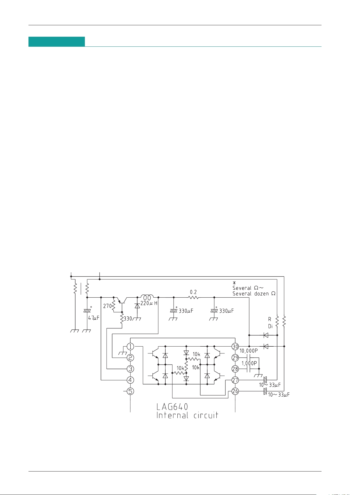
A diode for capacitor charging is connected between data transmission output pins 26 and 27 as shown
below; the surge current ratings shown below should not be exceeded.
If these ratings are to be exceeded, it is recommended that a resistance R for surge current limiting or a
diode Dt for absorption be inserted.
Internal diode maximum ratings Io 100mA
IF (peak) 500mA
IF (surge) 700mA
 Loading...