

Page 1

Ordering number : ENN6575
N2001RM (OT) No. 6575 -1/10
Overview
The LA9702W is an RF signal-processing and servo error
signal generation IC for DVD and CD playback. A DVD
player can be implemented by combining this IC with a
DVD DSP product that includes a digital servo DSP.
Functions and Features
• RF signal generation (with built-in gain adjustment
VGA circuit)
• RF peak detection and generation
• RF bottom detection and generation (with time constant
switching)
• Built-in RF equalizer amplifiers (two systems)
• FE amplifier (with built-in balance adjustment VCA and
offset cancellation pin)
• Three-beam TE amplifier (with built-in balance
adjustment VCA and offset cancellation pin)
• Reflection amplifier
• DPD circuit
• Tracking hold circuit
• Push-pull TE amplifier (with built-in balance adjustment
VCA)
• Built-in wobble detection bandpass filter
• APC circuits (two systems)
• Defect detection circuit
Package Dimensions
unit: mm
3220-SQFP80
14.0
12.0
1.25 1.25
0.5
14.0
12.0
1.25
1.25
0.5
120
21
40
41
60
61
80
0.1
0.5
1.6max
1.4
0.5
0.2
0.135
SANYO: SQFP80
[LA9702W]
LA9702W
SANYO Electric Co.,Ltd. Semiconductor Company
TOKYO OFFICE Tokyo Bldg., 1-10, 1 Chome, Ueno, Taito-ku, TOKYO, 110-8534 JAPAN
DVD Player Front End Processor
Monolithic Linear IC
Any and all SANYO products described or contained herein do not have specifications that can handle
applications that require extremely high levels of reliability, such as life-support systems, aircraft’s
control systems, or other applications whose failure can be reasonably expected to result in serious
physical and/or material damage. Consult with your SANYO representative nearest you before using
any SANYO products described or contained herein in such applications.
SANYO assumes no responsibility for equipment failures that result from using products at values that
exceed, even momentarily, rated values (such as maximum ratings, operating condition ranges, or other
parameters) listed in products specifications of any and all SANYO products described or contained
herein.
Parameter Symbol Conditions Ratings Unit
Maximum supply voltage V
CC
max 6.0 V
Allowable power dissipation Pd max Pdmax for ≤ 70°C (when mounted on a PCB) 500 mW
Operating temperature Topr –25 to +70 °C
Storage temperature Tstg –40 to +150 °C
Specifications
Maximum Ratings at Ta = 25°C
Note: These specifications are subject to change without notice.
Page 2

No. 6575 -2/10
LA9702W
Parameter Symbol Conditions
Ratings
Unit
min typ max
Current drain ICC No signal 40 58 75 mA
Reference voltage 1 PREF Pin 79, load current: ±2 mA 2.3 2.5 2.7 V
Reference voltage 2 SREF Pin 27, load current: ±2 mA 2.3 2.5 2.7 V
RF gain 1 RFG1
Input to pins 1 and 2, pin 21 = SREF – 0.75 V
0.25 3.25 6.25 dB
Pin 61 = pin 63 = pin 76 = 5 V, pins 40 and 41
RF gain 2 RFG2
Input to pins 1 and 2, pin 21 = REF + 0.75 V
18 21 24 dB
Pin 61 = pin 63 = pin 76 = 5 V, pins 40 and 41
PH PH
Pin 7 = pin 8 = pin 9 = 400 mVpp, pin 21 = SREF – 0.75 V
SREF + 0.4
SREF + 0.65
SREF + 0.9
V
Pin 61 = 5 V, pin 63 = pin 76 = 0 V, pin 44
BH BH
Pin 7 = pin 8 = pin 9 = 400 mVpp, pin 21 = SREF – 0.75 V
SREF – 0.08 SREF – 0.28 SREF – 0.48
V
Pin 57 = pin 59 = pin 61 = 5 V, pin 63 = pin 76 = 0 V, pin 42
RREC1 RREC1
Input to pins 3, 4, 5, and 6, pin 18 = SREF – 0.75 V,
4.2 9.2 14.2 dB
pin 76 = 5 V, Pin 28
RREC2 RREC2
Input to pins 3, 4, 5, and 6, pin 18 = SREF – 0.75 V,
20 23 26 dB
pin 76 = 5 V, Pin 28
RRECOST ROST
Pin 3 = pin 4 = pin 5 = pin 6 = PREF, pin 18 = SREF
SREF – 0.3
SREF
SREF + 0.3
V
Pin 76 = 5 V, pin 28
FEGAIN1 FEG1
Input to pins 3, 4, 5, and 6, pin 18 = SREF – 0.75 V,
13.9 17.9 21.9 dB
pin 76 = 5 V, Pin 29
FEGAIN2 FEG2
Input to pins 3, 4, 5, and 6, pin 18 = SREF + 0.75 V,
24 27 30 dB
pin 76 = 5 V, Pin 29
FEOST FOST
Pin 3 = pin 4 = pin 5 = pin 6 = PREF, pin 18 = SREF
SREF – 0.3
SREF
SREF + 0.3
V
Pin 76 = 5 V, pin 29
Input such that pin 3 = pin 5 and pin 4 = pin 6,
FEBAL1 FBAL1 pin 18 = SREF, Pin 76 = 5 V, pin 19 = SREF – 1 V, 3.7 6.7 9.7 dB
pin 29: ∆GAIN
Input such that pin 3 = pin 5 and pin 4 = pin 6,
FEBAL2 FBAL2 pin 18 = SREF, Pin 76 = 5 V, pin 19 = SREF + 1 V, –9.7 –6.7 –3.7 dB
pin 29: ∆GAIN
TEGAIN1 TEG1
Input to pin 10 and 11, pin 18 = SREF – 0.75 V,
11.8 15.8 19.8 dB
pin 63 = 0 V, Pin 68 = 0 V, pin 36
TEGAIN2 TEG2
Input to pin 10 and 11, pin 18 = SREF + 0.75 V,
26 29 32 dB
pin 63 = 0 V, pin 68 = 0 V, pin 36
TEOST TOST
Pin 10 = pin 11 = PREF, pin 18 = SREF, pin 63 = 0 V
SREF – 0.3
SREF
SREF + 0.3
V
Pin 68 = 0 V, pin 53 = 5 V, pin 36
TEBAL1 TBAL1
Input to pins 10 and 11, pin 18 = SREF, pin 63 = 0 V
4 7 10 dB
Pin 68 = 0 V, pin 20 = REF – 1 V, pin 36 ∆GAIN
TEBAL2 TBAL2
Input to pins 10 and 11, pin 18 = SREF, pin 63 = 0 V
–10 –7 –4 dB
Pin 68 = 0 V, pin 20 = REF + 1 V, pin 36 ∆GAIN
The difference in the pin 30 voltage between when
DPD phase difference
input with pin 1 = SREF, pin 2 = 5 MHz with 0° phase,
Voltage difference 1
PD1 pin 3 = 5 MHz with 36° phase, and when input with 0.25 0.37 0.48 V
pin 1 = SREF, pin 2 = 5 MHz with 36° phase,
pin 3 = 5 MHz with 0° phase. R
L
= 6.8 kΩ
The difference in the pin 30 voltage between when
DPD phase difference
input with pin 1 = SREF, pin 2 = 5 MHz with 0° phase,
Voltage difference 2
PD2 pin 4 = 5 MHz with 36° phase, and when input with –0.48 –0.37 –0.25 V
pin 1 = SREF, pin 2 = 5 MHz with 36° phase,
pin 4 = 5 MHz with 0° phase. R
L
= 6.8 kΩ
Electrical Characteristics/Operating Characteristics
at Ta = 25°C, VCC(pins 12, 55, and 66) = 5 V, ground (pins 17, 49, and 74) = 0 V
Parameter Symbol Conditions Ratings Unit
Recommended supply voltage Vcc 5.0 V
Operating supply voltage Vccop 4.5 to 5.5 V
Operating Conditions at Ta = 25°C
Continued on next page.
Page 3

No. 6575 -3/10
LA9702W
Continued from preceding page.
Parameter Symbol Conditions
Ratings
Unit
min typ max
The difference in the pin 30 voltage between when
DPD phase difference
input with pin 1 = SREF, pin 2 = 5 MHz with 0° phase,
Voltage difference 3
PD3 pin 5 = 5 MHz with 36° phase, and input with 0.25 0.37 0.48 V
pin 1 = SREF, pin 2 = 5 MHz with 36° phase,
pin 5 = 5 MHz with 0° phase. R
L
= 6.8 kΩ
The difference in the pin 30 voltage between when
DPD phase difference
input with pin 1 = SREF, pin 2 = 5 MHz with 0° phase,
Voltage difference 4
PD4 pin 6 = 5 MHz with 36° phase, and input with –0.48 –0.37 –0.25 V
pin 1 = SREF, pin 2 = 5 MHz with 36° phase,
pin 6 = 5 MHz with 0° phase. R
L
= 6.8 kΩ
DPD offset DPDOF Pin 1 = SREF, 2 = 3 = 4 = 5 = 5 MHz, R
L
= 6.8 kΩ
SREF – 0.5
SREF
SREF + 0.5
V
APC1 reference voltage LDS1 Pin 72 = 5 V 150 180 200 mV
APC1 off level LDD1 Pin 72 = 0 V 4.5 5 V
APC2 reference voltage LDS2 Pin 70 = 5 V 150 180 200 mV
APC2 off level LDD2 Pin 70 = 0 V 4.5 5 V
DFFTMU DEFTMU
Pin 2 = 80 kHz. The time difference from a pin 2 edge to
1.8 4 5.8 µS
the rising edge on pin 46.
DFFTMD DFFTMD
Pin 2 = 80 kHz. The time difference from a pin 2 edge to
100 500 µS
the falling edge on pin 46.
BPF1 BPF1 Pin 34 = 210 kHz, pin 32 –1 2 5 dB
BPF2 BPF2 Pin 34 = 120 kHz, pin 32 –20 –4 0 dB
BPF3 BPF3 Pin 34 = 3500 kHz, pin 32 –20 –6.5 –1 dB
Page 4

Functional Description
1. RF amplifier
• DVD mode
The RF signal input as a differential signal to pins 1 and 2 is passed through the RF VCA and is output from pin 65.
The signal output from pin 65 is passed through a DVD RF equalizer and is output to later stage ICs from pins 40 and
41. When pin 63 is high, the RF signal does not pass through the customer amplifier. As a result, it is not influenced by
the external peripheral circuit connected to pins 78 through 80. The RF VCA gain is controlled by applying a DC
voltage to pin 21. This IC provides two RF equalizer systems, and when pin 61 is high the pin 77 equalizer output is
selected, and when low, the pin 52 equalizer output is selected. The amount of boost provided by the RF equalizer can
be modified with the pin 22 DC voltage.
• CD mode
Pins 8, 9, and 10 can be set to be the RF input pins by setting pin 76 low. The customer amplifier connected to pins 78
through 80 is enabled by setting pin 63 low, a CD equalizer circuit can be constructed on pins 78 through 80, and the
signal will not pass through the DVD RF equalizer. The RF VCA gain is controlled by applying a DC voltage to pin
21.
2. Peak hold/bottom hold
The envelope waveforms for the peak and bottom of the front end RF signal output from pins 40 and 41 are output
from pins 42 and 43. The envelope detection constants are set by the values of the resistors inserted between pins 43
and 39 and ground. The bottom hold detection constant can be increased by about a factor of 4 by setting pin 59 low.
The bottom hold band width is also be increased by about a factor of 2 by setting pin 57 low.
3. Defect detection
The RF signal input from the pickup is converted to binary by a limiter circuit. The binary signal time is observed with
a monostable multivibrator, and if there is no change in binary signal for over a certain fixed period, pin 46 is set high.
The time period of the monostable multivibrator is set by the value of the capacitor connected to pin 47 and the resistor
connected to pin 48.
4. RF equalizer
The CD RF equalizer is constructed from external components and the customer amplifier on pins 78 and 80, and
outputs to the RF VCA in the next stage.
This IC provides two DVD RF equalizer systems, one of which is formed from external components and pins 67, 69,
71, 73, 75, and 77, and the other system is formed from external components and pins 52, 54, 56, 58, 60, and 62. When
pin 61 is high, the equalizer system on pins 67, 69, 71, 73, 75, and 77 is selected, and when that pin is low, the
equalizer system on pins 52, 54, 56, 58, 60, and 62 is selected. Since the customer amplifier is excluded from the
signal path when pin 63 is high, the CD equalizer does not influence IC operation in DVD mode.
5. BCA
Peak envelope detection is applied to the previous stage RF signal output from pins 40 and 41. The result is converted
to binary by comparison with the BCA threshold and output from pin 45. The BCA threshold is input from external
circuits to pin 25.
6. Reflect amplifier
The signals input to pins 3, 4, 5, and 6 or pins 7, 8, and 9 are added with an summing amplifier. The pit component is
removed from the input signal with a low-pass filter. The summed signal is passed through a VCA that adjusts the
servo gain and output from pin 28. The VCA that adjusts the servo gain is controlled by the DC voltage applied to pin
18.
Note that when the pin 76 input is high, pins 3, 4, 5, and 6 are selected, and when low, pins 7, 8, and 9 are selected.
No. 6575 -4/10
LA9702W
Page 5

7. FE amplifier
The signal input from either pins 3, 4, 5, and 6 or pins 8 and 9 is first passed through an offset adjustment circuit and is
then passed through a balance adjustment VCA. Then either the calculation <(pin 3 + pin 5) – (pin 4 + pin 6)> or <pin
8 – pin 9> is performed. The result is passed through the servo gain adjustment VCA and output from pin 29. The gain
of the balance adjustment VCA is adjusted by the DC voltage input to pin 19. The offset adjustment can be adjusted by
the DC voltage applied to pin 23. The VCA that adjusts the servo gain is controlled by the DC voltage applied to pin
18.
Note that when the pin 76 input is high, pins 3, 4, 5, and 6 are selected, and when low, pins 8 and 9 are selected.
8. TE amplifier (for three-beam operation)
The current signal input to pin 10 and 11 is converted from a current to a voltage, passed through an offset adjustment
circuit, and passed through a balance adjustment VCA. Then the calculation <pin 11 – pin 10> is performed and the
result passed through a servo gain adjustment VCA. The result is output from pin 30 after band switching. The offset
adjustment can be adjusted by the DC voltage applied to pin 24. The gain of the balance adjustment VCA can be
adjusted by the DC voltage applied to pin 20. The VCA that adjusts the servo gain is controlled by the DC voltage
applied to pin 18. The band switching circuit is a low-pass filter with a cutoff frequency of 30 kHz when pin 57 is high
and 100 kHz when pin 57 is low. When pin 53 is low, pin 30 operates in hold mode.
Note that the three-beam TE is used when pin 68 is low.
9. DPD circuit
The phases of the signals input to pins 1 and 2, and the signals input to pins 3, 4, 5, and 6 are compared and the result
outputs from pin 30.
The phase comparison result signal is output as a current by the pin 38 constant-current charge pump and converted to
a voltage level by the external capacitor and resistor on pin 38. The voltage-converted signal is passed through a buffer
amplifier, is band limited by a band switching circuit, and is output from pin 30. The charge pump is turned off when
pin 51 is high. The band switching circuit is a low-pass filter with a cutoff frequency of 30 kHz when pin 57 is high
and 100 kHz when pin 57 is low. When pin 53 is low, pin 30 operates in hold mode.
Note that the DPD circuit is used when pin 63 will be high.
10. PP amplifier
The signals input to pins 3, 4, 5, and 6 are passed first through an offset adjustment circuit and then through a balance
adjustment VCA. The calculation <(pin 3 + pin 6) – (pin 4 – pin 5)> is performed. The result is passed through a servo
gain adjustment VCA and is output from pin 35 after band switching. The offset adjustment can be adjusted by the DC
voltage applied to pin 24. The gain of the balance adjustment VCA can be adjusted by the DC voltage applied to pin
20. The VCA that adjusts the servo gain is controlled by the DC voltage applied to pin 18.
Note that the PP amplifier is used when pin 68 will be high.
11. Wobble bandpass filter
The signal input to pin 34 is passed through a bandpass filter and output from pin 32. The frequency fo for the
bandpass filter can be modified with the external resistor on pin 33. When the pin 33 external resistor is 62 kΩ, fo will
be about 200 kHz.
12. APC circuit
A servo loop that holds the laser power fixed can be formed by inputting a monitor signal to pin 14 and connecting the
laser driver to pin 13. The laser can be turned off by setting pin 72 low.
Note that there are two APC systems, with the other system consisting of pin 16 as the monitor input pin, pin 15 as the
drive pin, and pin 70 as the laser off control pin.
13. Reference circuit
A voltage that is created by resistor dividing VCCby 2 is output from pin 26. The pin 26 voltage is buffered and output
from pins 79 and 27. The pin 79 voltage is a special-purpose reference voltage only for use by the pickup, and the pin
27 voltage is a reference supplied to the DSP and other systems.
No. 6575 -5/10
LA9702W
Page 6

No. 6575 -6/10
LA9702W
Pin Functions
Pin No. Pin Function
1 RFN RF signal – input
2 RFP RF signal + input
3 PD1 Pickup signal input
4 PD2 Pickup signal input
5 PD3 Pickup signal input
6 PD4 Pickup signal input
7 PD5 Pickup signal input
8 PD6 Pickup signal input
9 PD7 Pickup signal input
10 PD8 Pickup signal input
11 PD9 Pickup signal input
12 VCC Power supply (servo signal system)
13 LDD1 APC 1 output
14 LDS1 APC 1 monitor voltage input
15 LDD2 APC 2 output
16 LDS2 APC 2 monitor voltage input
17 GND Ground (servo signal system)
18 SGC Servo gain control (RREC, FE, and TE)
19 FEBL Focus balance adjustment
20 TEBL Tracking balance adjustment
21 VGA RF gain adjustment
22 BST Equalizer boost adjustment
23 FOST Focus offset adjustment
24 TOST Tracking offset adjustment
25 BCATH BCA threshold adjustment
26 REFI Reference voltage setting
27 SREF Servo signal reference voltage output
28 RREC Reflection output
29 FE Focus error output
30 TE Tracking error output
31 THC TE hold time constant setting capacitor connection
32 WO Wobble output
33 ISET Bandpass filter center frequency setting resistor connection
34 WOI Push-pull signal input
35 WOO Push-pull signal output
36 TEO Three-beam TE gain setting
37 TEN Three-beam TE gain setting
38 CP Charge pump gain setting resistor and capacitor connection
39 BHI Bottom hold detection constant setting resistor connection
40 RFON RF – output
41 RFOP RF + output
42 BH RF bottom detection output
43 PHI Peak hold detection constant setting resistor connection
44 PH RF peak detection output
45 BCA BCA output
46 DEF Defect output (High: defect detected)
47 DEFC Defect detection capacitor connection
48 TC Defect detection constant setting resistor connection
49 GND Ground (DPD system)
50 LPC RF DC servo capacitor connection
51 CPOF Charge pump on/off control (High: off)
52 EQO2 RF equalizer setting
53 TH Tracking hold (High: hold)
Continued on next page.
Page 7

No. 6575-7/10
LA9702W
Pin No. Pin Function
54 EQL2 RF equalizer setting
55 VCC Power supply (DPD system)
56 EQO4 RF equalizer setting
57 XHTR Tracking and bottom detection band switching (Low: high band)
58 EQI4 RF equalizer setting
59 XQBH Bottom detection time constant switching (Low: fast)
60 EQ03 RF equalizer setting
61 EQSCT Equalizer switching (High: pin 77 selected, low: pin 52 selected)
62 EQI3 RF equalizer setting
63 DPD/TE DPD/three-beam tracking switching (High: DPD)
64 RFO2 RF output
65 RFO1 RF output
66 VCC Power supply (RF system)
67 EQI1 RF equalizer setting
68 PP/TE Three-beam/push-pull tracking switching (Low: three-beam)
69 EQO1 RF equalizer setting
70 LDON2 APC 2 laser on/off control (High: on)
71 EQI2 RF equalizer setting
72 LDON1 APC 1 laser on/off control (High: on)
73 EQO2 RF equalizer setting
74 GND Ground (RF system)
75 EQL1 RF equalizer setting
76 RFSCT RF input switching (High: RF differential input, PP error)
77 EQO1 RF equalizer setting
78 CAO Customer amplifier output
79 PREF Reference voltage output (pickup)
80 CAN Customer amplifier input
Continued from preceding page.
Note: The equalizer constants support 1× and 2× speeds.
Page 8
LA9702W
No. 6575-8/10
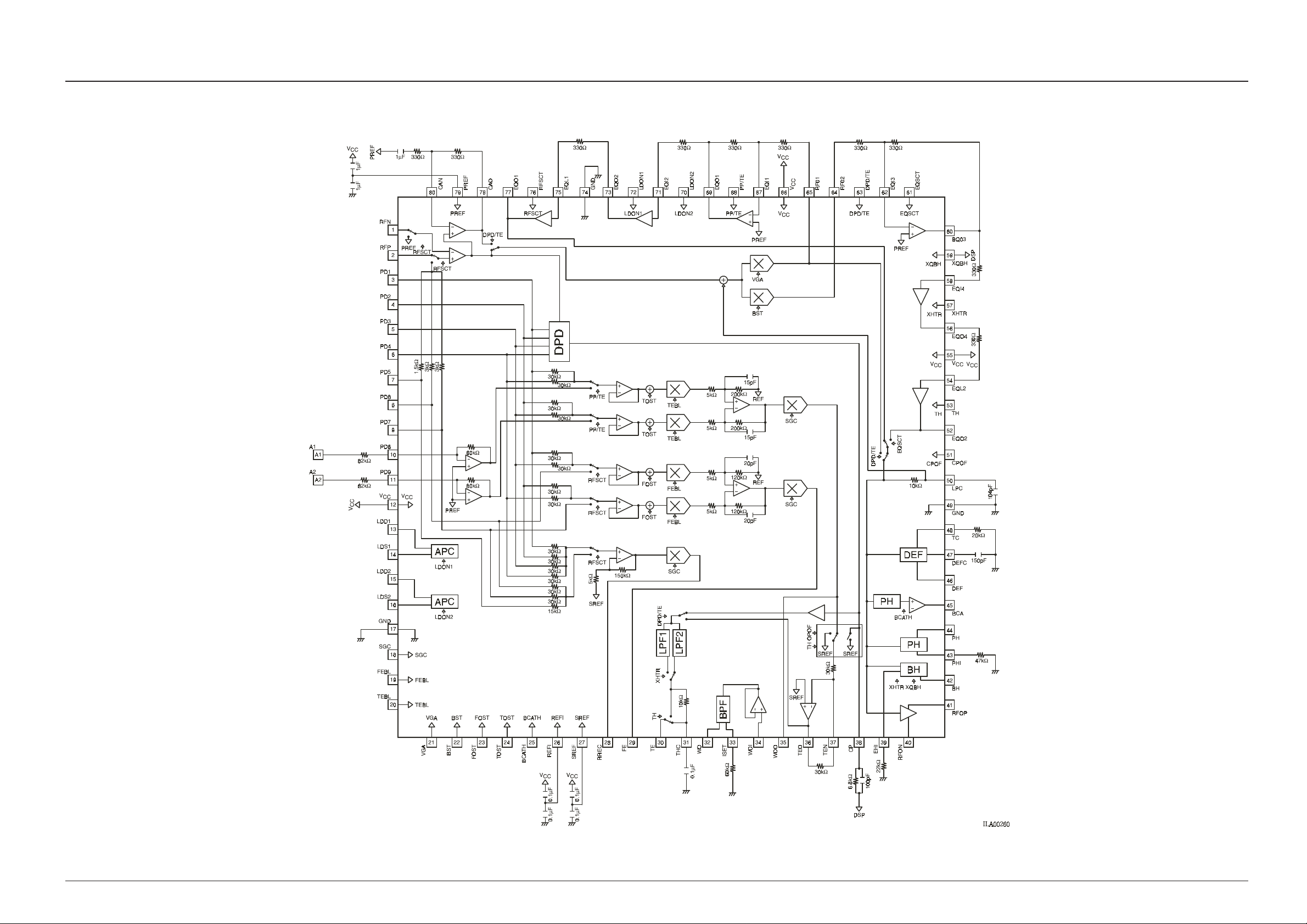
Test Circuit
Page 9
LA9702W
No. 6575-9/10
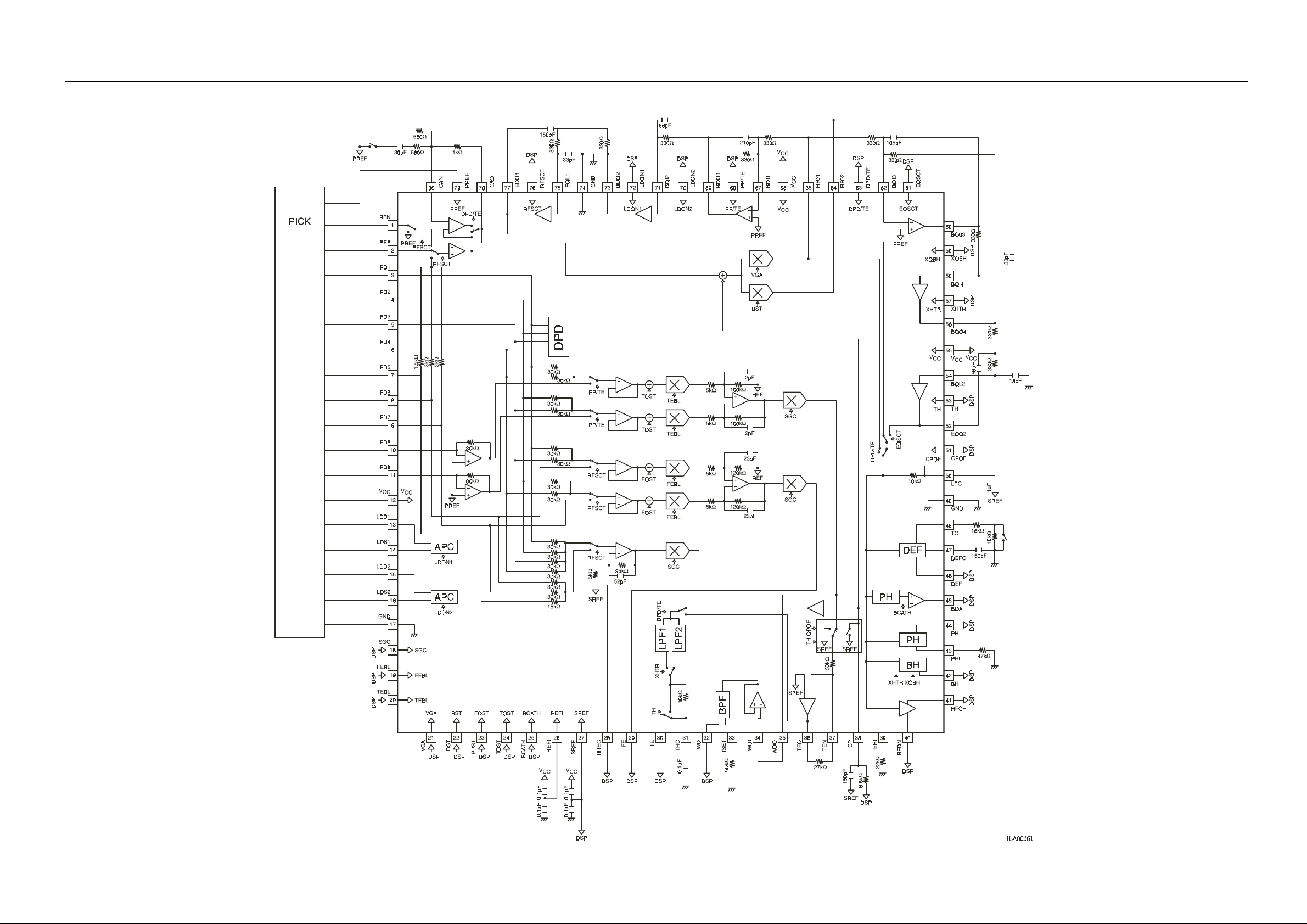
Sample Application Circuit
The equalizer constants support normal and 2× speeds.
Page 10
PS No. 6575 -10/10
LA9702W
This catalog provides information as of November, 2001. Specifications and information herein are
subject to change without notice.
Specifications of any and all SANYO products described or contained herein stipulate the performance,
characteristics, and functions of the described products in the independent state, and are not guarantees
of the performance, characteristics, and functions of the described products as mounted in the customer’s
products or equipment. To verify symptoms and states that cannot be evaluated in an independent device,
the customer should always evaluate and test devices mounted in the customer’s products or equipment.
SANYO Electric Co., Ltd. strives to supply high-quality high-reliability products. However, any and all
semiconductor products fail with some probability. It is possible that these probabilistic failures could
give rise to accidents or events that could endanger human lives, that could give rise to smoke or fire,
or that could cause damage to other property. When designing equipment, adopt safety measures so
that these kinds of accidents or events cannot occur. Such measures include but are not limited to protective
circuits and error prevention circuits for safe design, redundant design, and structural design.
In the event that any or all SANYO products (including technical data, services) described or contained
herein are controlled under any of applicable local export control laws and regulations, such products must
not be exported without obtaining the export license from the authorities concerned in accordance with the
above law.
No part of this publication may be reproduced or transmitted in any form or by any means, electronic or
mechanical, including photocopying and recording, or any information storage or retrieval system,
or otherwise, without the prior written permission of SANYO Electric Co., Ltd.
Any and all information described or contained herein are subject to change without notice due to
product/technology improvement, etc. When designing equipment, refer to the “Delivery Specification”
for the SANYO product that you intend to use.
Information (including circuit diagrams and circuit parameters) herein is for example only; it is not
guaranteed for volume production. SANYO believes information herein is accurate and reliable, but
no guarantees are made or implied regarding its use or any infringements of intellectual property rights
or other rights of third parties.
 Loading...