

Page 1
Ordering number: EN5177
Monolithic Linear IC
LA7583
(A
Overview
The LA7583 is a VIF + SIF IC that requires no adjustments. In
order to eliminate the need for adjustments in the VIF block, a
multi-network PLL has been developed and adopted for video
detection. In the SIF block, adjustments were eliminated by
using gyrator technology in the FM quadrature detector. In
addition to eliminating the need for adjustments, a buzz
canceller that suppresses Nyquist buzz has been built into the
LA7583 in order to provide excellent sound quality.
Features
.
Elimination of VCO, AFT, and SIF coils eliminates the need
for adjustments.
.
A variety of built-in filters.
.
Built-in buzz canceller results in excellent audio
characteristics.
2
Note: A
C Automatic Adjustment Control
AQT Automatic Quadrature Tuning
2
C PLL VIF + SIF) for TVs and VCRs
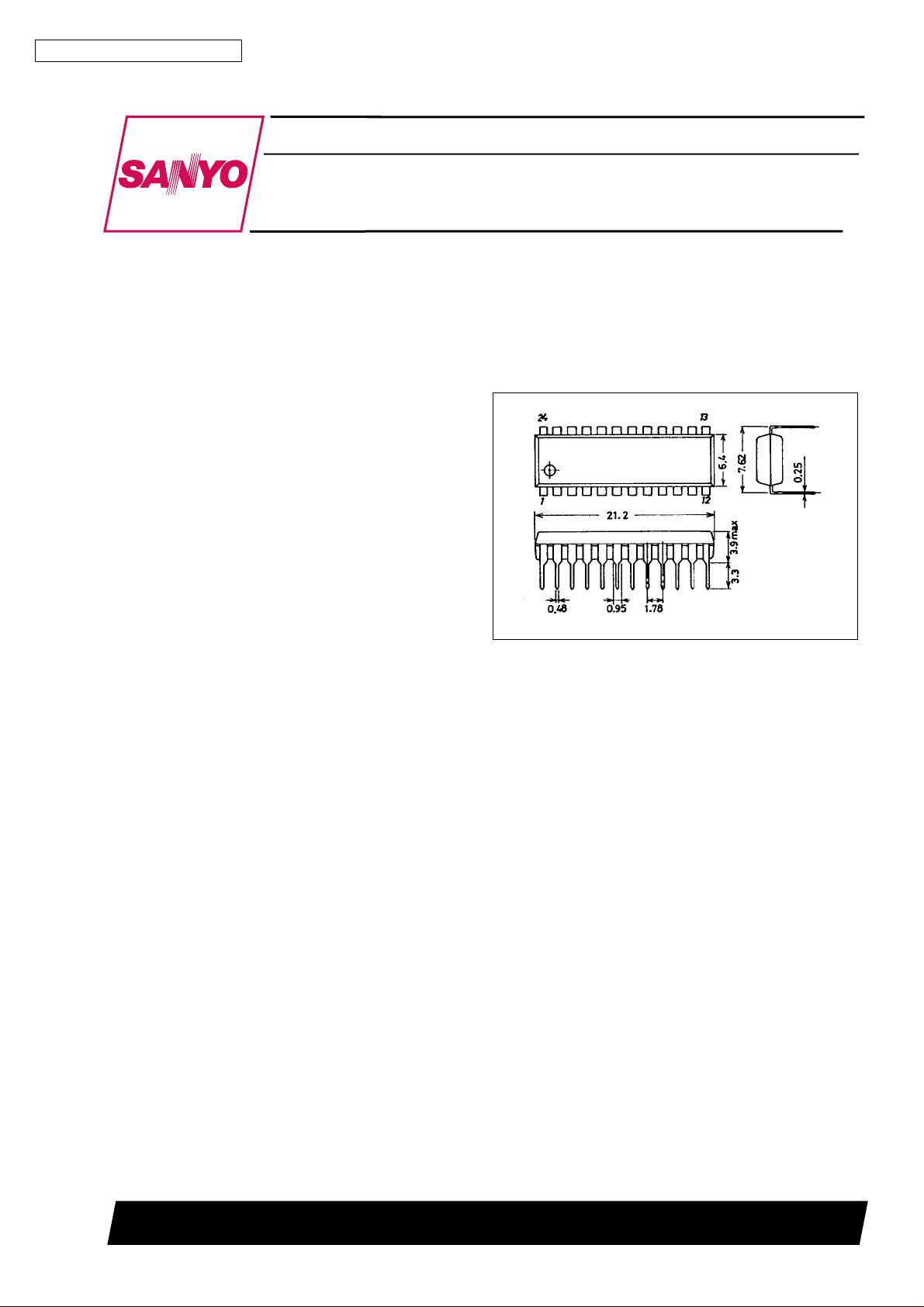
Package Dimensions
unit : mm
3067-DIP24S
[LA7583]
SANYO : DIP24S
IF Signal Processing Circuit
Functions
[VIF]
.
VIF amplifier
.
Equalizer amplifier
.
AGC lag lead filter
[1st SIF]
.
Preamplifier
[SIF]
.
Limiter amplifier
[mute]
.
Audio mute
.
Multinetwork PLL
.
AFT
.
Video driver
.
1st SIF detector
.
AQT detector (gyrator)
.
AV mute
.
BNC
.
IFAGC
.
AGC detector
.
J/U switch
.
FAGC
.
Buzz canceller
.
Built-in AGC filter
SANYO Electric Co.,Ltd. Semiconductor Bussiness Headquarters
TOKYO OFFICE Tokyo Bldg., 1-10, 1 Chome, Ueno, Taito-ku, TOKYO, 110 JAPAN
83095HA(II) No.5177-1/15
Page 2
LA7583
Specifications
Maximum Ratings atTa=25°C
Parameter Symbol Conditions Ratings Unit
V
17V
Maximum supply voltage
Circuit voltage
Circuit current I1, I10, I23 –1 mA
Allowable power dissipation Pd max T
Operating temperature Topr –20 to +70
Storage temperature Tstg –55 to +150
*A2C (Automatic Adjustment Control)
Note: Current flowing into the IC is positive (no signal) and current flowing out is negative.
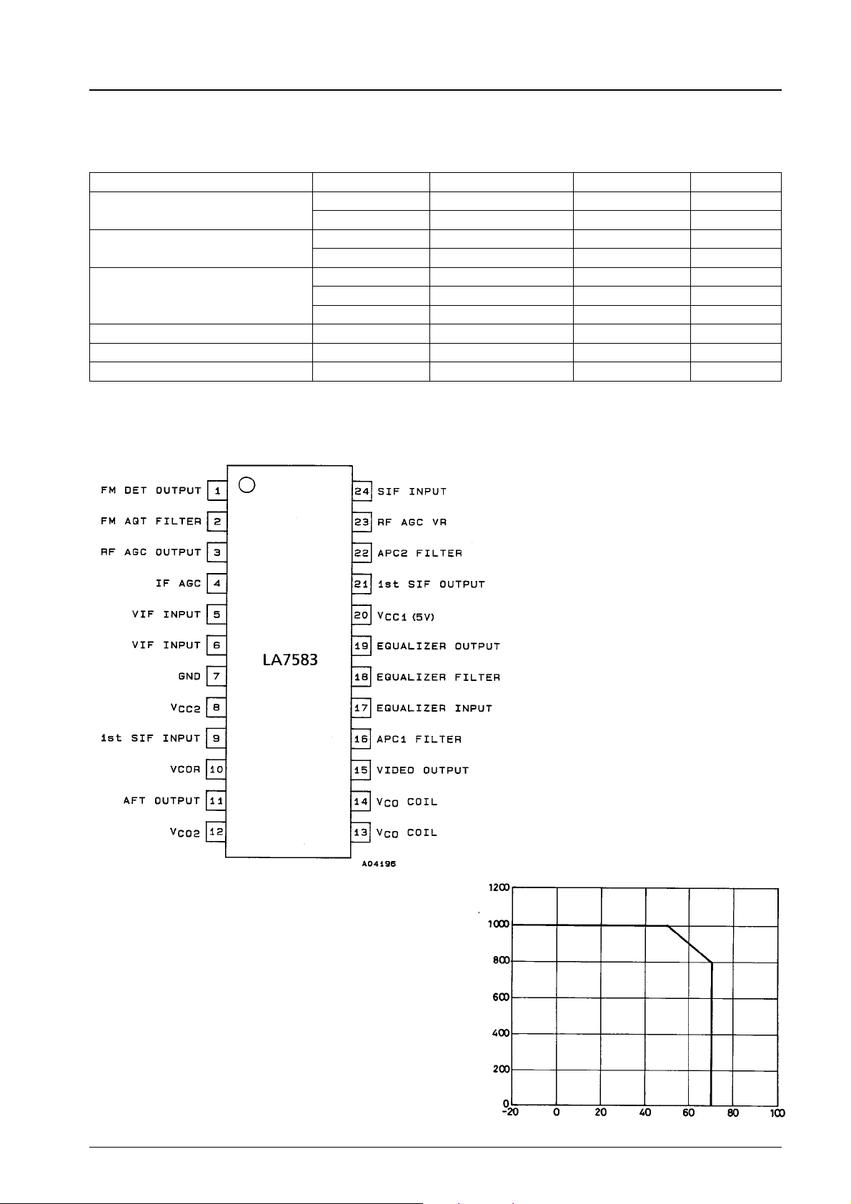
Pin Assignment
CC
V
2 13.2 V
CC
V4 V
V3, V11 V
I3, I21 –3 mA
I15, I19 –5 mA
% 50°C 1000 mW
a
1V
CC
2V
CC
C
°
C
°
Top View
Pd max — Ta
Allowable power dissipation, Pd max − mW
Ambient temperature, Ta −°C
No.5177-2/15
Page 3
LA7583
Operating Conditions atTa=25°C
Parameter Symbol Conditions Ratings Unit
V
15V
Recommended supply voltage
Operating supply voltage range
Electrical Characteristics atTa=25°C, VCC1=5V,VCC2 = 9 V, fp = 45.75 MHz
Parameter Symbol Conditions min typ max Unit
[VIF Block]
Circuit current 1 I20 V
Circuit current 2 I8 V
Maxinum RF AGC voltage V3H V4=3V 7.5 8.1 9 V
Mininum RF AGC voltage V3L V4 = 1.5 V 0 +0.5 V
Input sensitivity Vi S1 = OFF 32 38 44 dBµ
AGC range G
Maxinum Allowable Input Vi max 95 103 dBµ
Video output voltage
with no signal
Sync signal tip voltage V19(tip) Vi = 10 mV 1.1 1.4 1.7 V
Video output amplitude V
Black noise threshold level
voltage
Black noise clamp voltage V
Output S/N S/N 48 52 dB
920 kHz beat level I920 P = 0, C = –10 dB, S = –10 dB 41 45 dB
Frequency characteristics f
Differential gain DG Vi = 10 mV, 87.5% 3 8 %
Differential phase DP 10STAR STEP 3 8 rad
AFT output voltage
with no signal
Maxinum AFT output voltage V11H 7.5 8.5 9 V
Mininum AFT output voltage V11L 0 +1 +1.5 V
AFT detection sensitivity Sf 33 48 69
VIF input resistance Ri(VIF) f = 45.75 MHz 0.8 1.1 1.5 kΩ
VIF input capacity Ci(VIF) f = 45.75 MHz 2 3 5 pF
APC pull-in range (U) f
APC pull-in range (L) f
AFT crossover frequency ∆f
VCO1 maximum variable range
VCO2 maximum variable range
VCO1 control sensitivity β1 V22 = 2.8 V to 3.2 V 2.4 4.8 9.6
VCO2 control sensitivity β2 V16 = 2.8 V to 3.2 V 0.3 0.6 1.2
[1st SIF Block]
4.5 MHz output gain VG Vi=1mV,41.25 MHz 23 26 29 dB
4.5 MHz output level SO Vi = 10 mV, 41.25 MHz 50 85 120 mVrms
1st SIF maximum input level Si (max) So + 12 dB–1dB 60 70 mVrms
1st SIF input resistance Ri (SIF1) f = 41.25 MHz 1.2 2 kΩ
1st SIF input capacity Ci (SIF1) f = 41.25 MHz 3 6 pF
R
V19 V4=2V 3.3 3.6 3.9 V
(V) 87.5% mod 1.7 2.0 2.3 Vp-p
O
V
BTH
BCL
C
V11 0.3 4.5 8.7 V
PU
PL
A
∆f
1 V22=4V 2.0 5.0 MHz
U
∆f
1 V22=2V –5.0 –2.0 MHz
L
∆f
2 V16=4V 100 200 kHz
U
∆f
2 V16=2V –1000 –200 kHz
L
CC
V
29V
CC
V
1 4.6 to 6 V
CC
V
2 7 to 12 V
CC
= 5 V 57 66 78 mA
CC
= 9 V 7.8 11.0 14.0 mA
CC
56 62 dB
0.4 0.7 1.1 V
1.65 1.95 2.25 V
P = 0, S = –14 dB 6 8 MHz
mV/kHz
1.0 3 MHz
–4.5 –1.0 MHz
–65 +65 kHz
kHz/mV
kHz/mV
Continued next page.
No.5177-3/15
Page 4

LA7583
Continued from preceding page.
Parameter Symbol Conditions min typ max Unit
[SIF Block]
SIF limiting sensitivity Vi (lim) ∆f = 25 kHz, 400 Hz 47 53 59 dBµ
FM detection output voltage V
AMR AMR AM = 30%, 400 Hz 40 56 dB
Total harmonic distortion THD ∆f = 25 kHz, 400 Hz 0.4 1.5 %
SIF S/N S/N(SIF) ∆f = 25 kHz, 400 Hz 55 59 dB
[Mute defeat]
FM mute V24T 0.5 1.0 V
AFT defeat voltage VD11 3.9 4.5 5.1 V
J/U SW start voltage VJU24 1.5 2.0 2.5 V
AV mute voltage VM23 1 1.5 V
Vi = 100 mV, ∆f = 25 kHz, 400 Hz 300 400 520 mVrms
O
No.5177-4/15
Page 5
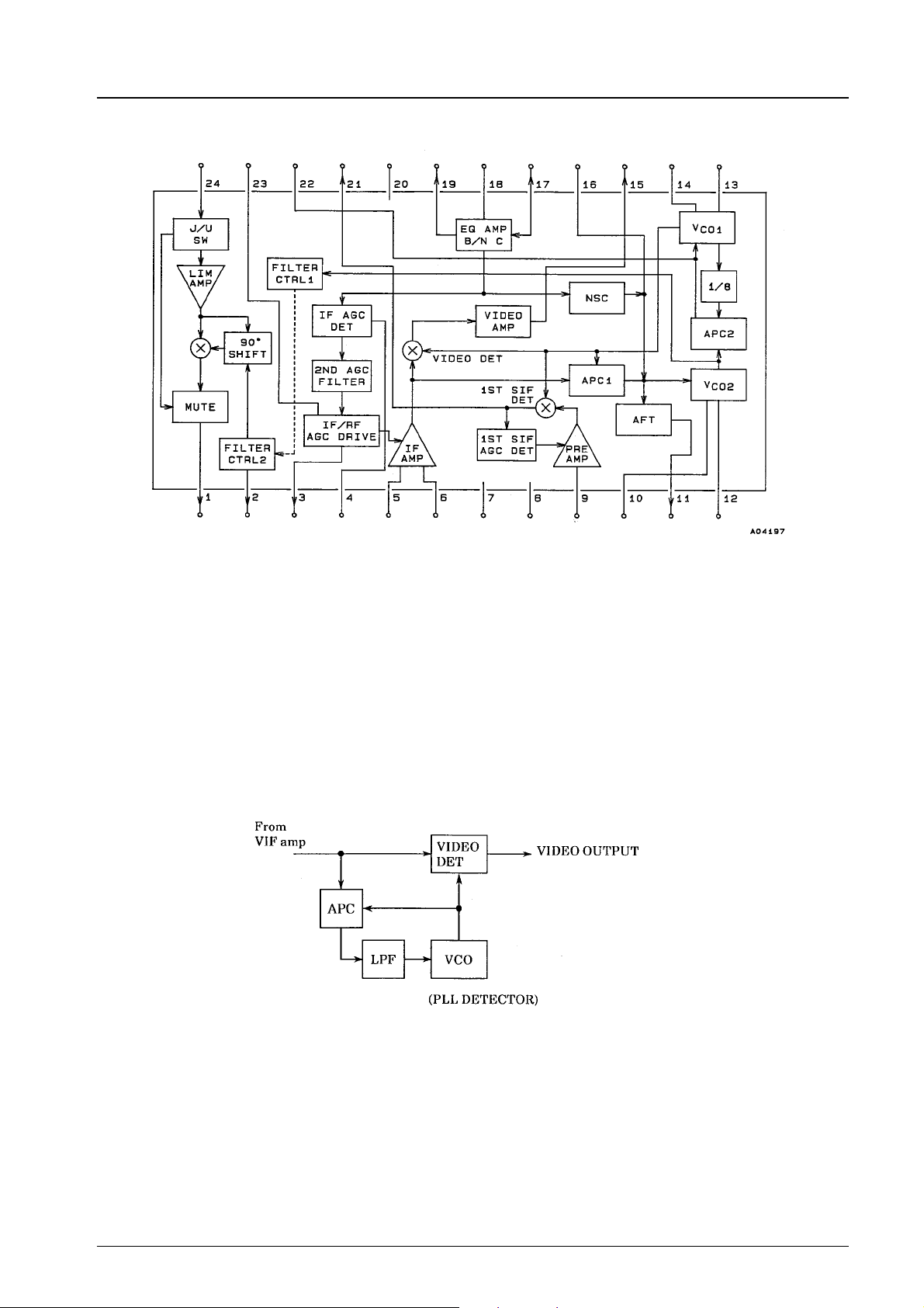
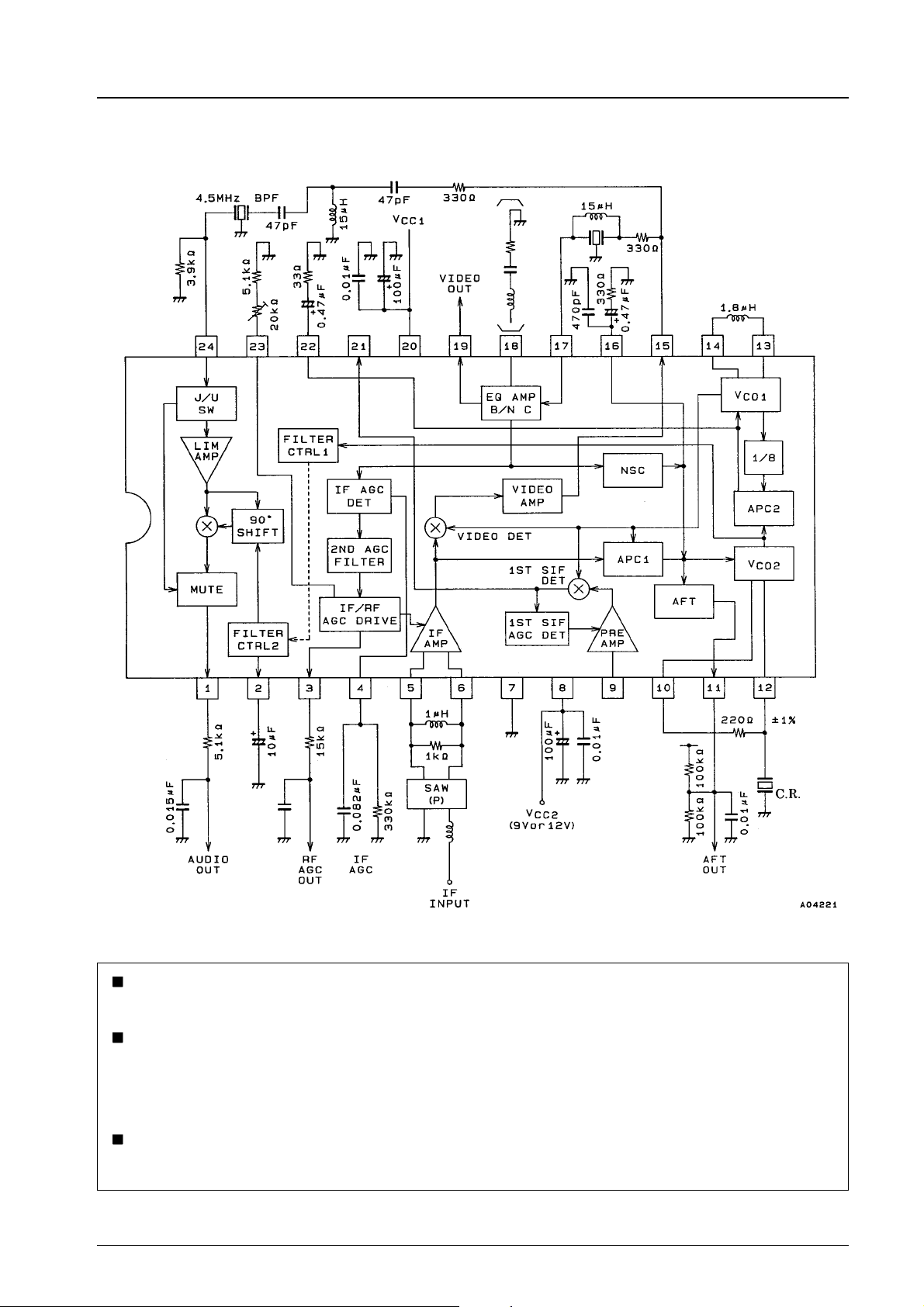
Equivalent Circuit Block Diagram
LA7583
Multinetwork PLL (Automatic Adjustment Control)
The LA7583’s PIF detector uses a multinetwork PLL and a buzz canceller. The multinetwork PLL is a PLL detector that was
developed in order to eliminate the need for adjustments in video detection.
This PLL detector offers the following features:
(1) Eliminates the need for adjustments in video detection.
(2) The PLL detection characteristics are unaltered.
a. Offers better waveform response characteristics in comparison with the quasi-synchronous detection method.
b. The harmonic wave component of the video signal (demodulated output) is reduced.
c. The 1/2 IF signal suppression ratio is improved.
(3) Audio buzz is greatly reduced by the buzz canceller.
A typical PLL detector consists of the blocks shown below.
In these blocks, if the VCO coil is not adjusted to the IF frequency, a phase difference will appear in the control loop. As a result,
the PLL detector detection axis will shift from the ideal 180°. The group delay, DP characteristics, etc., deteriorate as a result.
No.5177-5/16
Page 6
LA7583
[Multinetwork PLL]
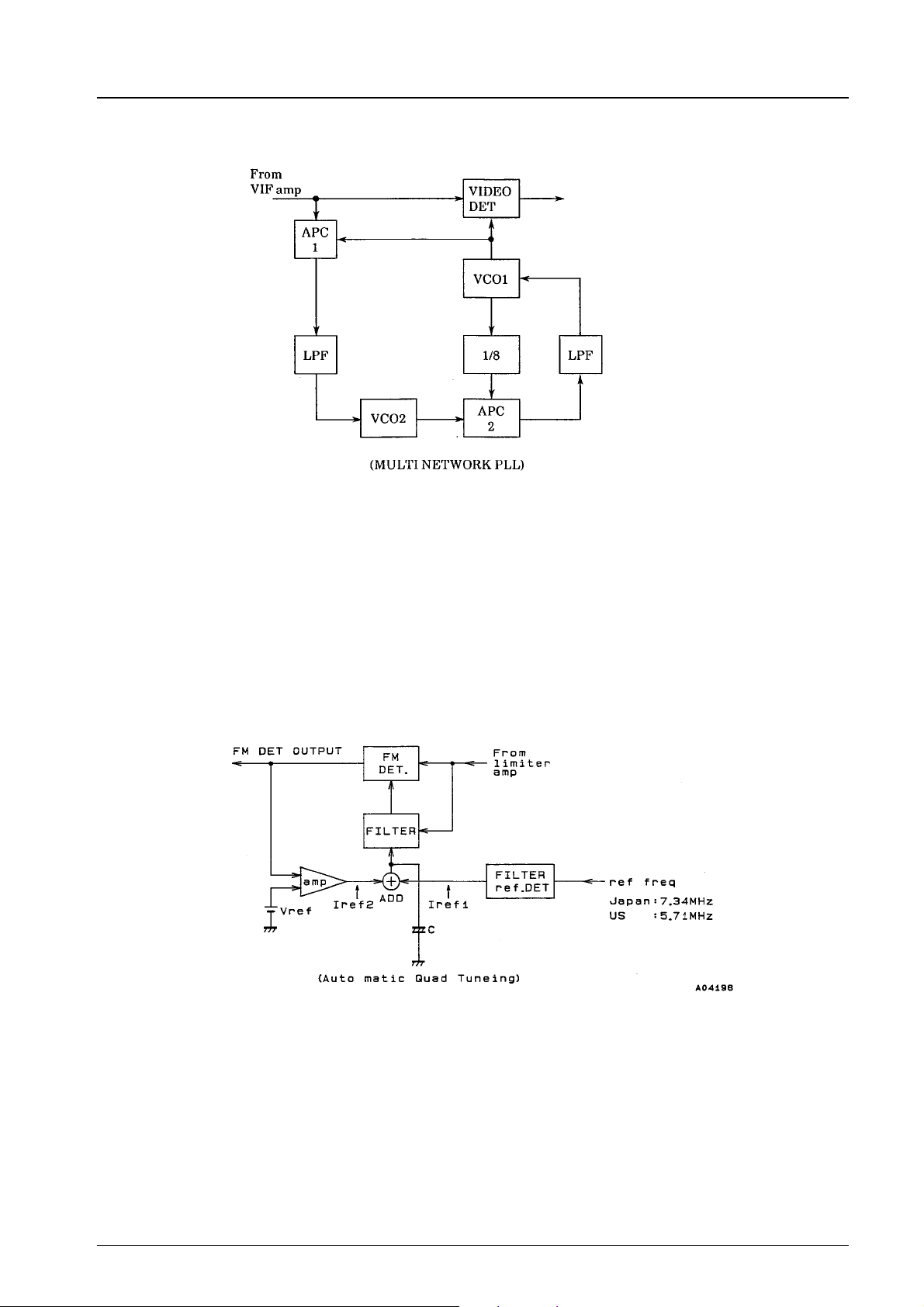
The multinetwork PLL consists of the blocks shown below.
The multinetwork PLL has two VCO circuits. Each of these form a separate PLL. The operational relationship between these
circuits is as follows:
f
VCO1=fVCO2
Initially, in APC1, the phases of the IF signal and the VCO carrier are compared. The control signal derived is then used to
control VCO2. VCO1 is controlled by comparing the phases of VCO2 and VCO1 x 1/8. As a result, VCO1 always has the same
frequency as the IF signal, and the following relationship results:
f
VCO1=fVCO2
If the precision of the ceramic oscillator for f
phase error is very small. As a result, the multinetwork PLL operates as an ideal PLL detector.
× 8
× 8
is within the adjustment range for VCO in a typical PLL, the video detector
VCO2
Automatic Quadrature Tuning (AQT)
A quadrature detector that is controlled automatically is used in the FM detector. The AQT in the LA7583 consists of the blocks
shown in the following diagram.
The FM detection filter (gyrator) is controlled at 4.5 MHz by the control current (Iref1) generated by reference circuit 1. At the
same time, precision control is performed by using the control current (Iref2) derived by detecting the offset from the detected
output so that the FM detector phase relationship is 90°. As a result, automatic control makes an ideal quadrature detector
possible.
(Note) Gyrator: Circuit-formed equivalent inductance
The SIF circuit contains a 4.5 MHz tank circuit having the gyrator and an internal capacitor.
No.5177-6/15
Page 7
Pin Functions
LA7583
Pin
No.
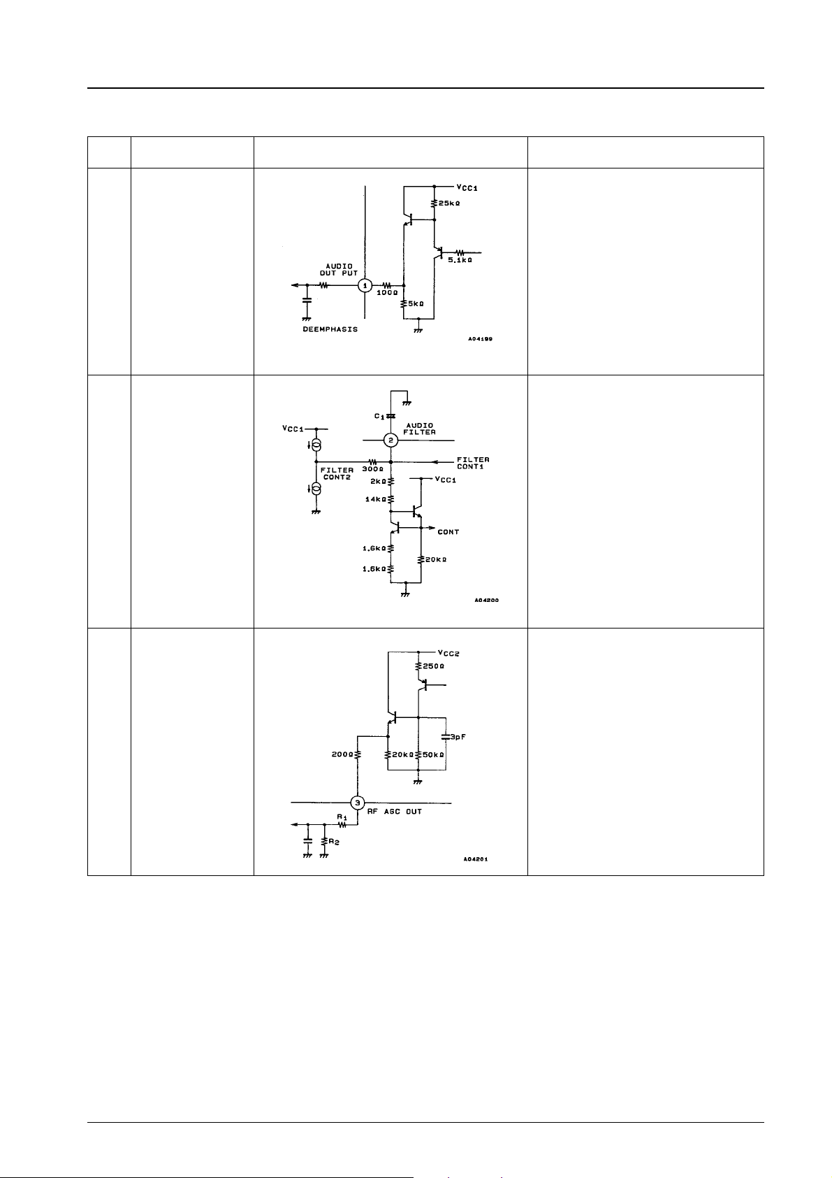
1 FM DETECTOR
2 FM AQT FILTER
Symbol Circuit Configuration Description
OUTPUT
GYLATOR
Pin 1 is an audio FM output pin. A 100 Ω
resistor is connected in series with the
emitter follower.
(1) Monaural applications
CR are used to form a de-emphasis
cicuit externally.
t = CR1
(2) Audio multiplexing applications
Depending on the audio multiplexing
decoder application, the input
impedance is low, which may distort the
L-R signals, etc., and degrade the
stereo characteristics. In such an event,
add a resistor between pin 1 and GND.
R2 ^ 5.1 kΩ
Pin 2 is the FM Automatic Quadrature
Tuning filter pin. This pin controls the
quadrature detector so that it remains at its
center frequency (4.5 MHz), and is the point
where the two control currents are added.
If the value of external capacitor C1 is small,
the low-range frequency characteristics
deteriorate. If the capacitance is too large,
the low-range characteristics improve, but
the response characteristics at SW-ON, etc.,
worsen.
The recommended value for C1 is 10 µF to
33 µF.
3 RF AGC OUTPUT
Pin 3 is the RF AGC output pin. It is an
emitter output, and a protective resistor of
200 Ω is connected between pin 3 and
emitter.
This pin determines the resistance bleeder
(R1, R2) values according to the maximum
gain of the tuner.
Continued on next page.
No.5177-7/15
Page 8

Continued from preceding page.
LA7583
Pin
No.
4 IF AGC
56VIF INPUT
Symbol Circuit Configuration Description
Pin 4 is the 1st IFAGC filter pin. This filter
smoothes out the peaks detected in the
signal by the AGC detector, and generates
the AGC voltage. The 2nd AGC filter (lag
lead filter) is built in using filter technology.
The cutoff frequency is approximately
500 Hz.
.
AGC filter constants and AGC speed
Medium-speed AGC: R1 = 330 kΩ
High-speed AGC: R1 = 470 kΩ
Pins 5 and 6 are the VIF amplifier input
pins. The VIF amplifier has three stages,
each of which uses a C cut, so when used
in conjunction with a SAW filter, DC cut by a
capacitor becomes unnecessary.
Ri = 1.1 kΩ
Ci=3pF
C1 = 0.1 µF
C1 = 0.056 µF
9 1st SIF INPUT
Pin 9 is the 1st SIF input pin. Input is such
that DC cut must be performed using a
capacitor. When a SAW filter, etc. is used in
the input circuit, an L that is used to
neutralize the SAW filter output capacitance
and the IC input capacitance serves to
improve the 1st SIF sensitivity.
Continued on next page.
No.5177-8/15
Page 9
Continued from preceding page.
LA7583
Pin
No.
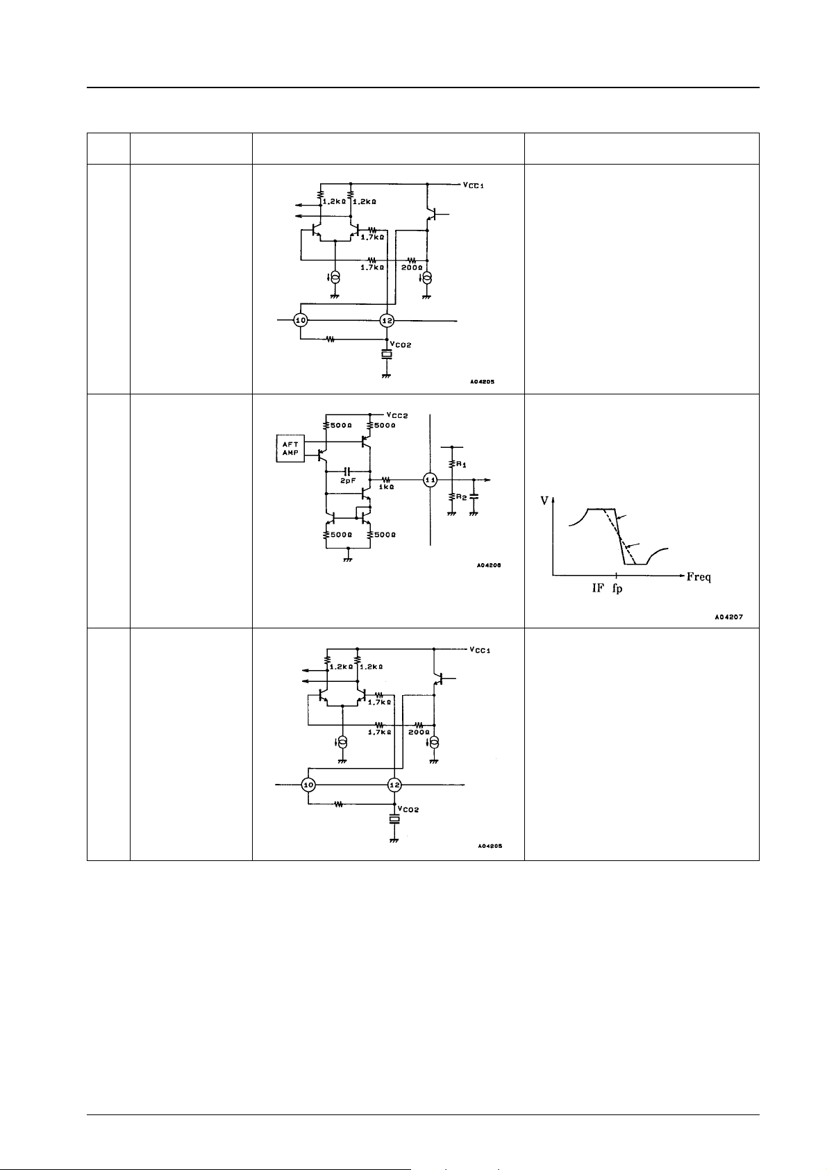
10 VCOR
11 AFT OUTPUT
Symbol Circuit Configuration Description
Pin 10 is the pin for connecting the resistor
that determines the impedance of the
oscillation point of the oscillating circuit by
the ceramic oscillator. Oscillation frequency
variations can be reduced by connecting a
resistor with a tolerance of 1% between pin
10 and pin 12.
Pin 11 is the AFT output pin. This pin
determines the gain (control sensitivity: β
(kHz/mV)) according to the R1 and R2
bleeder resistance values. β is decreased in
weak electric fields by AGC voltage in order
to reduce malfunction of AFT. R1 and R2
must be 200 kΩ or less.
AFT curve for medium/
strong electric fields
AFT curve for weak
electric fields
12 VCO2
Pin 12 is the ceramic oscillator (VCO2) pin.
A series resonance-type oscillator is used to
oscillate 1/8 of the IF signal.
Japan = 58.75 MHz × 1/8
U.S. = 45.75 MHz × 1/8
Continued on next page.
No.5177-9/15
Page 10
Continued from preceding page.
LA7583
Pin
No.
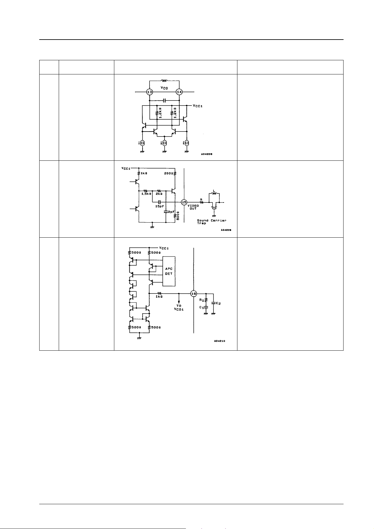
1314VCO COIL
15 VIDEO OUTPUT
16 APC1 FILTER
Symbol Circuit Configuration Description
Pins 13 and 14 are the VCO tank circuit.
VCO coil recommended
.
Japan 1.2 µH
.
U.S. 1.8 µH
Make the circuit pattern between the IC and
the coil as short as possible.
Pin 15 is the SIF carrier (4.5 MHz)-contained
video output pin. The level of the video
output is approximately 1.5 Vp-p.
Pin 16 is the APC1 filter pin. The filter
smoothes the output after comparing the
phase of the IF signal with that of VCO1 in
APC1.
C
= 0.47 µF
1
R
= 330 to 560Ω
1
C
= 470 pF
2
Continued on next page.
No.5177-10/15
Page 11
Continued from preceding page.
LA7583
Pin
No.
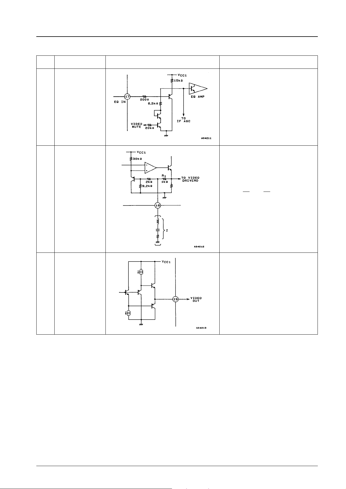
17 EQUALIZER INPUT
18 EQUALIZER FILTER
Symbol Circuit Configuration Description
Pin 17 is the equalizer amplifier input pin. A
signal which has passed through a 4.5 MHz
trap is input through pin 17 and is output
through pin 19.
.
The input level of pin 17 is 1.5 Vp-p. This
is amplified 3 dB to 2 Vp-p by the
equalizer amplifier.
Pin 18 is the equalizer pin. The equalizer
amplifier is of the voltage follower type with
a voltage gain of 3 dB. To correct the
frequency characteristics, connect LCR
externally.
The operating characteristics are as follows:
Av =
Ve
Vi
=1+
R1
Z
(times)
19 EQUALIZER
OUTPUT
Pin 19 is the equalizer amplifier output pin.
This output has a built-in low-impedance
drive circuit.
Continued on next page.
No.5177-11/15
Page 12
Continued from preceding page.
LA7583
Pin
No.
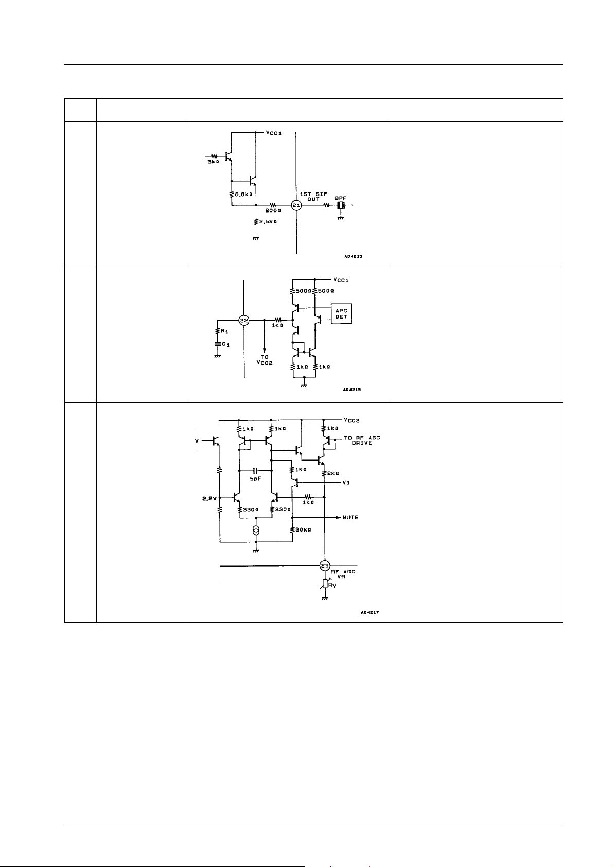
21 1st SIFOUT
22 APC2 FILTER
Symbol Circuit Configuration Description
Pin 21 is the 1st SIF output pin. The SIF
carrier output level is approximately
50 mVrms.
Pin 22 is the APC2 filter pin. The filter
smoothes the output after comparing the
phase of VCO2 with that of VCO1 x 1/8 in
APC2.
C
= 0.47µF
1
R
=33Ω
1
23 RF AGC VR
Pin 23 is the RF AGC adjusting pin. The
adjustment point is where Rv approximates
15 kΩ. AV (audio/video) mute is effected by
dropping this pin to GND.
Continued on next page.
No.5177-12/15
Page 13
Continued from preceding page.
LA7583
Pin
No.
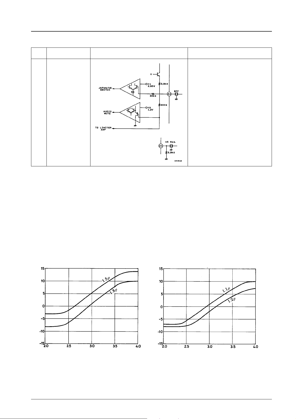
24 SIF INPUT, J/U SW
LA7583 VCO COIL design considerations
1. Design criteria
Allow for an adequate variable range for the IF frequency in the design. Specifically, select a coil value so that the carrier
frequency is roughly in the center of the characteristics diagram shown below when 2 V and 4 V are applied to pin 22.
Symbol Circuit Configuration Description
Pin 24 is used both for SIF input and J/U
SW audio mute.
.
The input impedance is approximately
1.5 kΩ.
.
J/U (Japan/U.S.) switch
The oscillating frequency for VCO2 in
Japan and the U.S. differs. However, the
center frequency of the SIF detector is
controlled using VCO2 as a reference. As
a result, the filter control mode can be
changed either by leaving this pin open or
dropping it to GND through a 3.9 kΩ
resistor.
Open: Japan mode
3.9 kΩ: U.S. mode
.
Audio mute:
Audio muting can be applied by dropping
the voltage on this pin to 0.5 V or less.
2. Design notes
a. When selecting the L value, the LA7583 must be soldered directly on the board. If an IC socket is used, an error in the VCO
center frequency will arise from the capacitance of the socket.
b. The patterns for pins 13 and 14 must be made as short as possible (15 mm or less). Minimize the effect of the printed
pattern.
c. A VCO coil of which tolerance is ± 5% must be used.
3. Measuring the IF frequency range
Drop the IF AGC (pin 4) to GND. Next, pick up the VCO carrier leak at a pin other than the VCO coil (pins 13 and 14) and
read the carrier frequency. And then, apply a voltage ranging from 1.5 V to 4.5 V to pin 22, and record the characteristics of the
maximum variable frequency range for VCO as shown in the diagram below.
US fO: 45.75 MHz JAPAN fO: 58.75 MHz
− MHz
O
f
− MHz
O
f
Y22−V Y22−V
4. Recommended VCO coil
A. Tokyo Parts Industry Co., Ltd. 5LC JAPAN 1.2 µH ± 5%
U.S. 1.8 µH ± 5%
No.5177-13/15
Page 14
LA7583
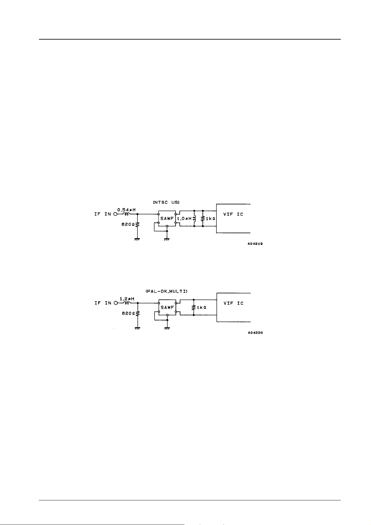
Notes on Sanyo SAW Filters
There are two types of filters, depending on the piezoelectric substrate material.
(1) LiTaO
(2) LiNbO
(lithium tantalate) SAW filters: .......TSF1xxx
3
TSF2xxx
While the LiTaO
SAW filters offer excellent stability with a low temperature coefficient of –18 ppm/°C, the insertion
3
loss is high. However, by using a coil, etc., to obtain proper matching on the SAW filter output side (which does increase
the number of external components), it is possible to suppress the insertion loss while at the same time making the level
of the characteristics variable, which provides additional design freedom. (Refer to Fig. 13.) In addition, because the SAW
(surface wave) reflection is small, ripple within the band can be kept low.
(lithium niobate) SAW filter: ......TSF5xxx
3
While the LiNbO
dB compared to the LiTaO
SAW filter has a high temperature coefficient of –72 ppm/°C, it has a lower insertion loss by about 10
3
SAW filters. Therefore, matching on the output side of the SAW filter is not necessary. (Refer
3
to the diagram below.) In addition, because the insertion loss is low (although the ripple within the band is somewhat
higher than in the case of the LiTaO
SAW filter), the low impedance and small feedthrough diminish the effects of
3
peripheral circuit components and the pattern layout, and make it possible to stabilize the trap characteristics outside of
the band.
LiTaO
LiNbO
From the above, it is clear that the LiTaO
high, while the LiNbO
SAW Filter
3
SAW Filter
3
SAW filter is suitable for PAL and U.S. bands where the IF frequency is low.
3
SAW filter is suitable for Japan and U.S. bands where the IF frequency is
3
(a) Picture wide BAND SAW Filter
Japan TSF1137U
U.S. TSF1241U(with IS-31 Trap)
(b) INTER Carrier SAW Filter
Japan TSF1138P
U.S. TSF1220P
No.5177-14/15
Page 15
Test circuit Diagram
LA7583 (U.S.)
LA7583
*2
*1
*1. TDK ceramic oscillator FCR5.71M2SF3
*2. Micro-inductor 5LC1R8, made by Tokyo Parts Industry Co., Ltd.
No products described or contained herein are intended for use in surgical implants, life-support systems, aerospace equipment,
nuclear power control systems, vehicles, disaster/crime-prevention equipment and the like, the failure of which may directly or
indirectly cause injury, death or property loss.
Anyone purchasing any products described or contained herein for an above-mentioned use shall:
1 Accept full responsibility and indemnify and defend SANYO ELECTRIC CO., LTD., its affiliates, subsidiaries and distributors
and all their officers and employees, jointly and severally, against any and all claims and litigation and all damages, cost and
expenses associated with such use:
2 Not impose any responsibility for any fault or negligence which may be cited in any such claim or litigation on SANYO
ELECTRIC CO., LTD., its affiliates, subsidiaries and distributors or any of their officers and employees jointly or severally.
Information (including circuit diagrams and circuit parameters) herein is for example only; it is not guaranteed for volume
production. SANYO believes information herein is accurate and reliable, but no guarantees are made or implied regarding its use
or any infringements of intellectual property rights or other rights of third parties.
This catalogprovidesinformationasofAugust, 1995. Specifications and information herein are subject to change without notice.
No.5177-15/15
 Loading...