

Page 1
Overview
The LA7566 is a VIF/SIF IC that supports PAL and
NTSC multisound and that adopts a semi-adjustment-free
system. To simplify adjustment, the VIF block adopts a
technique in which AFT adjustment is no longer required
by VCO adjustment. The SIF block supports audio multidetection by adopting a PLL detection technique. The SIF
block provides 4 inputs with IC internal switching for easy
design of multi-sound systems. Additionally, these
switches can also be used for video system sound trap
switching. The LA7566 also includes a buzz canceller that
suppresses Nyquist buzz to achieve improved audio
quality.
Functions
[VIF Block]
• VIF amplifier • PLL detector • BNC • RF AGC
• EQ amplifier • AFT • IF AGC • Buzz canceller
[First SIF Block]
• First SIF amplifier • First SIF detector • AGC
[SIF Block]
• Multiple input switch • Limiter amplifier • PLL FM
detector
Features
• No coils are used in the AFT and SIF blocks, making
these circuits adjustment free.
• PAL / NTSC multisound system can be constructed
easily.
• Built-in buzz canceller for excellent audio performance
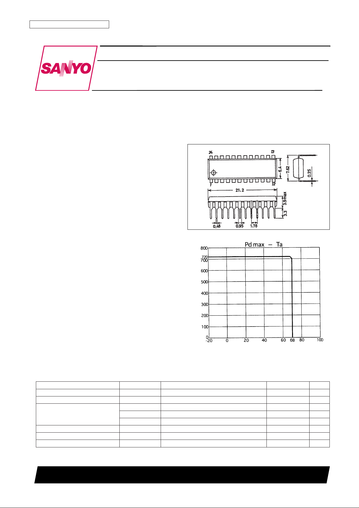
Package Dimensions
unit: mm
3067-DIP24S
Monolithic Linear IC
31398HA (OT) No. 5764-1/11
SANYO: DIP24S
[LA7566]
SANYO Electric Co.,Ltd. Semiconductor Bussiness Headquarters
TOKYO OFFICE Tokyo Bldg., 1-10, 1 Chome, Ueno, Taito-ku, TOKYO, 110-8534 JAPAN
VIF/SIF IF Signal-Processing Circuit with TV/VCR PAL
and NTSC Multisound Support
LA7566
Ordering number : EN5764
Ambient temperature, Ta — °C
Parameter Symbol Conditions Ratings Unit
Maximum supply voltage V
CC
max 10 V
Circuit voltage V7, V9, V10, V17 V
CC
V
I1 –2 mA
Circuit current I13 –3 mA
I18 –10 mA
Allowable power dissipation Pd max 720 mW
Operating temperature Topr –20 to +70 °C
Storage temperature Tstg –55 to +150 °C
Specifications
Maximum Ratings at Ta = 25°C
Allowable power dissipation, Pd max — W
Page 2

No. 5764-2/11
LA7566
Parameter Symbol Conditions Ratings Unit
Recommended supply voltage V
CC
9 V
Operating supply voltage range V
CC
op 4.6 to 9.5 V
Operating Conditions at Ta = 25°C
Parameter Symbol Conditions
Ratings
Unit
min typ max
[VIF Block]
Circuit current I3 45 53 61 mA
Maximum RF AGC voltage V9H 7.5 8.1 V
Minimum RF AGC voltage V9L 0 0.5 V
Input sensitivity V
IN
S1 = OFF 28 34 40 dBµV
AGC range G
R
45 50 dB
Maximum allowable input V
IN
max 95 100 dBµV
No-signal video output voltage V13 3.7 4.0 4.3 V
Sync tip voltage V13 tip 1.3 1.6 1.9 V
Video output level V
O
1.7 2.0 2.3 Vp-p
Black noise threshold voltage V
BTH
0.7 1.0 1.3 V
Black noise clamp voltage V
BCL
2.0 2.3 2.6 V
Video signal-to-noise ratio S/N 48 52 dB
C-S beat IC-S 44 49 dB
Frequency characteristics f
C
6 MHz –3 –1.5 dB
Differential gain DG 3 8 %
Differential phase DP 3 8 deg
Maximum AFT voltage V10H 7.5 8.5 9.0 V
Minimum AFT voltage V10L 0 0.2 1.0 V
AFT detection sensitivity Sf 29 37 47 mV/kHz
VIF input resistance Ri 38.9 MHz 1.5 kΩ
VIF input capacitance Ci 38.9 MHz 3 pF
APC pull-in range (U) f
PU
1.0 1.5 MHz
APC pull-in range (L) f
PL
–1.5 –0.8 MHz
AFT tolerance frequency 1 dfa1 –500 0 +500 kHz
VCO 1 maximum variability range (U) dfu 1.7 2.0 MHz
VCO 1 maximum variability range (L) dfl –2 –1 MHz
VCO control sensitivity B 1.15 2.3 4.6 kHz/mV
[First SIF Block]
Conversion gain VG 32 35 38 dB
5.5 MHz output level S
O
84 87 90 mVrms
Maximum first SIF input S
IN
max 85 88 91 mVrms
First SIF input resistance R
IN
(SIF) 33.4 MHz 2 kΩ
First SIF input capacitance C
IN
(SIF) 33.4 MHz 3 pF
[SIF Block]
Limiting sensitivity VIi(lim) 43 49 dBµV
FM detector output voltage V
O
(FM) 5.5 MHz ± 30 kHz 390 500 630 mVrms
AM rejection ratio AMR 50 60 dB
Total harmonic distortion THD 0.2 1.5 %
SIF S/N S/N (FM) 55 60 dB
[SIF Switch Block] Switches A, B, and C: H = open, L = ground
NTSC mode 6-dB amplifier NTSW 5 6 7 dB
SIF crosstalk 21 CT21 51 57 dB
SIF crosstalk 22 CT22 51 57 dB
SIF crosstalk 23 CT23 51 57 dB
SIF crosstalk 24 CT24 51 57 dB
Switch threshold low-level voltage SW (L) 1.0 1.5 V
Operating Characteristics at Ta = 25°C, VCC= 9 V, fp = 38.9 MHz
Page 3
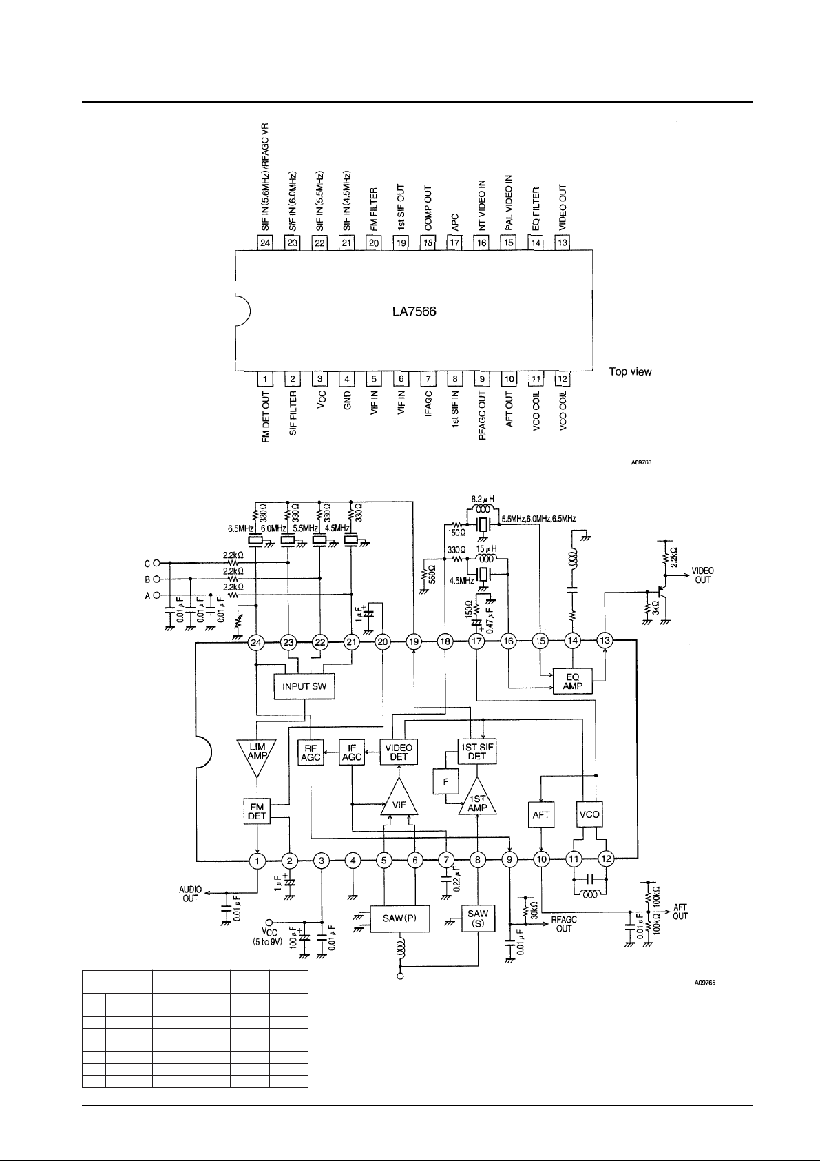
Pin Assignment
No. 5764-3/11
LA7566
Application Circuit Diagram
H : OPEN
L : GND
Switch
5.5 MHz 6.0 MHz 6.5 MHz 4.5 MHz
A B C
H H H
●●
H H L ●●
H L H ●●
H L L ●●
L H H ●● ●● ●●
L L L ●● ●● ●● ●●
L H L ●● ●●
L L H ●● ●●
Page 4

Internal Equivalent Circuit Diagram
No. 5764-4/11
LA7566
Page 5
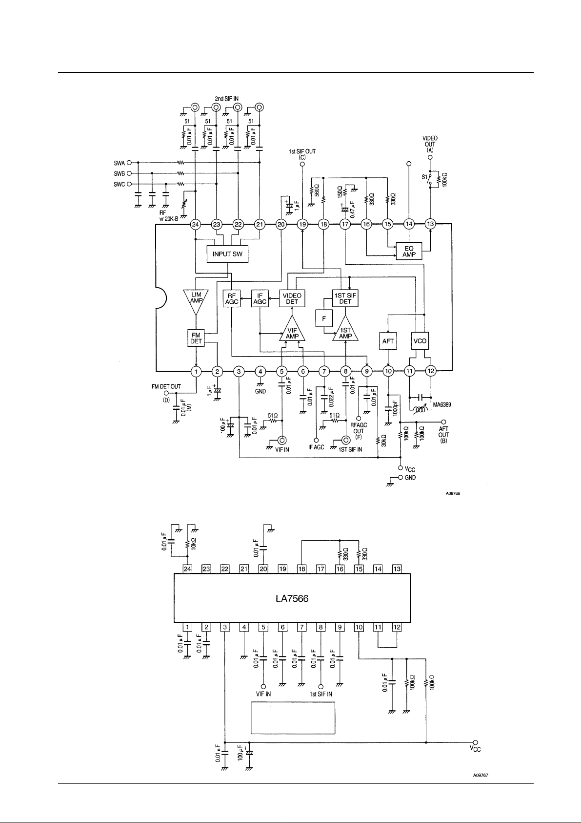
AC Characteristics Test Circuit Diagram
No. 5764-5/11
LA7566
Test Circuit
Input Impedance Test Circuit (VIF and first SIF input impedance)
Impedance analyzer
Page 6

No. 5764-6/11
LA7566
Pin No. Symbol Pin function Equivalent circuit
Pin Functions
1 FM DET OUT
• Audio FM detector output.
Deemphasis is switched internally in the IC. (5 kΩ and 7.5 kΩ)
This switching is linked to the SIF input switch. An external
emitter-follower circuit must be provided if the deemphasis is
disabled.
2 SIF FILTER
• Connection for a filter that holds the FM detector output DC
voltage at a fixed level. Normally, a 1-µF electrolytic capacitor is
used. To improve the low band (around 50 Hz) frequency
characteristics, increase the value of this capacitor (C1).
5
6
VIF IN
• VIF amplifier input.
The input circuit is constructed as a balanced input, and the
input has the following impedance characteristics:
R ≈ 1.5 kΩ
C ≈ 3 pF
Continued on next page.
Page 7

No. 5764-7/11
LA7566
Continued from preceding page.
Pin No. Symbol Pin function Equivalent circuit
7 IF AGC
• IF AGC filter connection.
The AGC voltage is created at pin 7 from the signal to which
peak detection was applied by the internal AGC detector.
Additionally, the IC includes an internal second AGC filter (a
lag-lead filter) used to create a dual time constant. A 0.022 µF
capacitor is used as the external capacitor. The value of this
capacitor must be adjusted according to measurement of the
sag, AGC speed, and other circuit aspects.
8 1st SIF IN
• First SIF input.
A DC cut capacitor must be inserted in the input to this circuit.
When a SAW filter is used: The first SIF sensitivity can be
increased by inserting an inductor between the SAW and the IC
to match the SAW output and IC input capacitances.
When an intercarrier system is used: This pin must be
connected to ground through a capacitor.
9 RF AGC OUT
• RF AGC output.
This output controls the tuner RF AGC. This is an open-
collector output with an inserted 100-Ω protective resistor.
Determine the value of the external bleeder resistor to match
the tuner specifications.
10 AFT OUT
• AFT output.
The AFT center voltage is created with an external bleeder
resistor. The AFT gain increases as the value of this bleeder
resistor increases. The value of this resistor must not exceed
390 kΩ. This circuit includes a control function that controls the
AFT voltage to be equal to the center voltage in weak field
reception conditions.
Continued on next page.
Page 8

No. 5764-8/11
LA7566
Continued from preceding page.
Pin No. Symbol Pin function Equivalent circuit
11
12
VCO
• VCO tank circuit used for video detection.
See the separately provided documentation for the tank circuit
coil (inductor) specifications.
13
14
VIDEO OUT
EQ FILTER
• Equalizer circuit. This circuit corrects the video signal frequency
characteristics.
• Notes on equalizer amplifier design:
The equalizer amplifier is designed as a voltage follower
amplifier with a gain of about 2.3 dB. When the frequency
characteristics are corrected, connect an inductor, a capacitor,
and a resistor in series between pin 14 and ground.
The equalizer amplifier gain is given by:
R1
AV = ——+ 1
Z
Here, R1 is an IC internal resistor with a value of 1 kΩ. Select Z
according to the desired characteristics. However, care is
required to prevent distortion at the resonant point determined
by Z, where the gain is maximum.
15
16
PAL VIDEO IN
NT VIDEO IN
• Equalizer amplifier inputs.
Pin 15 is for PAL, and pin 16 for NTSC format signals. These
inputs are linked to and switched by the SIF switches.
17
APC FILTER
• PLL detector APC filter connection.
The APC time constants are switched internally in the IC. When
locked, the VCO is controlled over the path A, and the loop gain
is reduced. When unlocked and during weak field reception, the
VCO is controlled over the path B, thus increasing the loop
gain.
We recommend values of:
R = 150 to 390 Ω, and
C = 0.47 µF
for the loop filter constants.
Continued on next page.
Page 9

No. 5764-9/11
LA7566
Continued from preceding page.
Pin No. Symbol Pin function Equivalent circuit
18 COMP OUT
• Output for the video signal that includes the SIF carrier.
A resistor must be inserted between pin 18 and ground to
acquire an adequate drive capability.
R ≥ 470 Ω
19 1st SIF OUT
• First SIF output
The signal output from this pin is passed through a bandpass
filter and input to the SIF circuit. This is an emitter-follower
output.
20 FM FILTER
• The FM detector signal-to-noise ratio can be improved by
inserting a filter in the FM detector bias line.
C1 should have a value of 0.47 µF or greater, and 1 µF is
recommended .
If the FM detector is not used, pin 20 must be connected to
ground through a 2-kΩ resistor. This stops the FM detector
VCO circuit.
21
22
23
24
SIF IN (4.5 MHz)
SIF IN (5.5 MHz)
SIF IN (6.0 MHz)
SIF IN (6.5 MHz)
RF AGC VR
• SIF inputs.
Four input pins are provided to support multi-side systems, and
a switching function is also included. Since buzzing and bass
beating can occur if interference signals, such as the video
signal or the chrominance signal, enter these pins, extra care
must be taken in designing the input circuit pattern layout. Note
that pin 24 also functions as the RF AGC adjustment pin. This
pin sets the tuner RF AGC operating point. Also, the FM output
and the video output can be muted at the same time by setting
this pin to the ground level.
Switch
5.5 MHz 6.0 MHz 6.5 MHz 4.5 MHz
A B C
H H H ●●
H H L ●●
H L H ●●
H L L ●●
L H H ●● ●● ●●
L L L ●● ●● ●● ●●
L H L ●● ●●
L L H ●● ●●
Page 10

Notes on Sanyo SAW Filters
There are two types of SAW filters, which differ in the piezoelectric substrate material, as follows:
1. Lithium tantalate (LiTaO3) SAW filter
TSF11 ■■ ■■ ■■ ······ Japan
TSF12 ■■ ■■ ■■ ······ US
Although lithium tantalate SAW filters have the low temperature coefficient of –18 ppm/°C, they suffer from a large
insertion loss. However, it is possible, at the cost of increasing the number of external components required, to minimize
this insertion loss by using a matching circuit consisting of coils and other components at the SAW filter output. At the
same time as minimizing insertion loss, this technique also allows the frequency characteristics, level, and other aspects
to be varied, and thus provides increased circuit design flexibility. Also, since the SAW filter reflected wave level is
minimal, the circuit can be designed with a small in-band ripple level.
2. Lithium niobate (LiNbO3) SAW filter
TSF52 ■■ ■■ ■■ ······ US
TSF53 ■■ ■■ ■■ ······ PAL
Although lithium niobate SAW filters have the high temperature coefficient of –72 ppm/°C, they feature an insertion loss
about 10 dB lower than that of lithium tantalate SAW filters. Accordingly, there is no need for a matching circuit at the
SAW filter output. Although the in-band ripple is somewhat larger than with lithium tantalate SAW filters, since they
have a low impedance and a small field slew, they are relatively immune to influences from peripheral circuit
components and the geometry of the printed circuit board pattern. This allows stable out-of-band trap characteristics to be
acquired. Due to the above considerations, lithium tantalate SAW filters are used in applications for the US and Japan
that have a high IF frequency, and lithium niobate SAW filters are used in PAL and US applications that have a low IF
frequency.
Notes on SAW Filter Matching
In SAW filter input circuit matching, rather than matching the IF frequency, flatter video band characteristics can be
acquired by designing the tuning point to be in the vicinity of the audio carrier rather than near the chrominance carrier.
The situation shown in figure on the right makes it easier to acquire flat band characteristics than that in figure on the left.
No. 5764-10/11
LA7566
Frequency
Tokyo Parts Industrial Co., Ltd. 236 Hinode Machi Isesaki Shi, Gunma Prefecture Japan TEL: +81-270-23-3731
Coil Specifications
JAPAN f = 58.75 MHz US f = 45.75 MHz PAL f = 38.9 MHz
VCO coils
Test production No. 16991A Test production No. 16687A Test production No. 16686A
Tokyo Parts Industrial Co., Ltd. Tokyo Parts Industrial Co., Ltd. Tokyo Parts Industrial Co., Ltd.
Picture Picture Picture
SAW filters (split) TSF1137U TSF1241 TSF5315
SOUND SOUND SOUND
SAW filters (inter)
TSF5220 TSF5321
TSF5221 TSF5344
SAW filter characteristics
The high-band reduced
The high-band is
extended
Frequency
With the tuning set to the IF frequency With the tuning set to the vicinity of S and C
Page 11

PS No. 5764-11/11
LA7566
Notes on VCO Tank Circuits
1. Built-in capacitor VCO tank circuits
When the power is turned on, the heat generated by the IC is transmitted through the printed circuit board to the VCO
tank circuit. At this point, the VCO coil frame functions as a heat sink and the IC heat is dissipated. As a result, it
becomes more difficult to transmit heat to the VCO tank cricuit's built-in capacitor, and the influence of drift at power
on is reduced. Therefore, it suffices to design the circuit so that the coil and capacitor thermal characteristics cancel.
Ideally, it is better to use a coil with a core material that has low temperature coefficient characteristics.
2. External capacitor VCO tank circuits
When an external capacitor is used, heat generated by the IC is transmitted through the printed circuit board directly
to the VCO tank circuit external capacitor. While this capacitor is heated relatively early after the power is turned on,
the coil is not influenced as much by this heat, and as a result the power-on drift is increased. Accordingly, a coil
whose core material has low temperature coefficient characteristics must be used. It is also desirable to use a
capacitor with similarly low temperature coefficient characteristics.
Note: Applications that use an external capacitor here must use a chip capacitor. If an ordinary capacitor is used,
problems such as the oscillator frequency changing with the capacitor orientation may occur.
This catalog provides information as of March, 1998. Specifications and information herein are subject to
change without notice.
■ No products described or contained herein are intended for use in surgical implants, life-support systems, aerospace
equipment, nuclear power control systems, vehicles, disaster/crime-prevention equipment and the like, the failure of
which may directly or indirectly cause injury, death or property loss.
■ Anyone purchasing any products described or contained herein for an above-mentioned use shall:
➀ Accept full responsibility and indemnify and defend SANYO ELECTRIC CO., LTD., its affiliates, subsidiaries and
distributors and all their officers and employees, jointly and severally, against any and all claims and litigation and all
damages, cost and expenses associated with such use:
➁ Not impose any responsibility for any fault or negligence which may be cited in any such claim or litigation on
SANYO ELECTRIC CO., LTD., its affiliates, subsidiaries and distributors or any of their officers and employees
jointly or severally.
■ Information (including circuit diagrams and circuit parameters) herein is for example only; it is not guaranteed for
volume production. SANYO believes information herein is accurate and reliable, but no guarantees are made or implied
regarding its use or any infringements of intellectual property rights or other rights of third parties.
 Loading...