

Page 1

Overview
The LA7437, 7437A is a video signal processing singlechip IC that handles the PAL-G, B and I, 4.43 NTSC, and
MESECAM formats. IC internal trimming is used to make
the LA7437, 7437A is completely adjustment free, and in
combination with a special-purpose CCD (the
LC89973M) it provides a significant reduction in external
components, including the glass delay line. Thus the
LA7437, 7437A can significantly reduce the signal
processing board manufacturing costs. Furthermore, the
LA7437, 7437A supports the NAP format (NTSC to PAL
conversion) that is poised to become widespread in
Europe, China and other markets.
Features
• Completely adjustment free
The AGC, carrier, deviation, and PB-Y level are
adjustment free.
The YC record current can also be made adjustment free
by using the LA7437, 7437A as the head amplifier.
• Support for NAP and PAL color array correction
Full modulation using a balanced modulator allows
playback and conversion to PAL format of NTSC
signals recorded on tape.
• Crosstalk exclusion in combination with a specialpurpose CCD
Crosstalk can be excluded without using a glass delay
line by combining the LA7437, 7437A with a specialpurpose CCD (the LC89973M).
• Minimal number of external components
New built-in components:
— Detail enhancer CR
— C-trap in the Y low-pass filter
— Playback C low-pass filter
• High performance and multiple functions
Linear phase picture controller
Double high-pass noise canceller, high-speed AFC,
DCC
New built-in functions
— NAP circuit
— AVNS (advanced vertical noise suppresor)
— Automatic QH insertion
— FM AGC
• Miniature package (42-pin DIP)
Package Dimensions
unit: mm
3025B-DIP42S
Monolithic Linear IC
41096HA (OT) No. 5473-1/8
SANYO: DIP42S
[LA7437, 7437A]
SANYO Electric Co.,Ltd. Semiconductor Bussiness Headquarters
TOKYO OFFICE Tokyo Bldg., 1-10, 1 Chome, Ueno, Taito-ku, TOKYO, 110 JAPAN
Video Signal Processing IC
for VHS VCR Systems
LA7437, 7437A
Ordering number : EN5473
Page 2
No. 5473-2/8
LA7437, 7437A
Functions
All VHS format VCR signal processing functions
Specifications
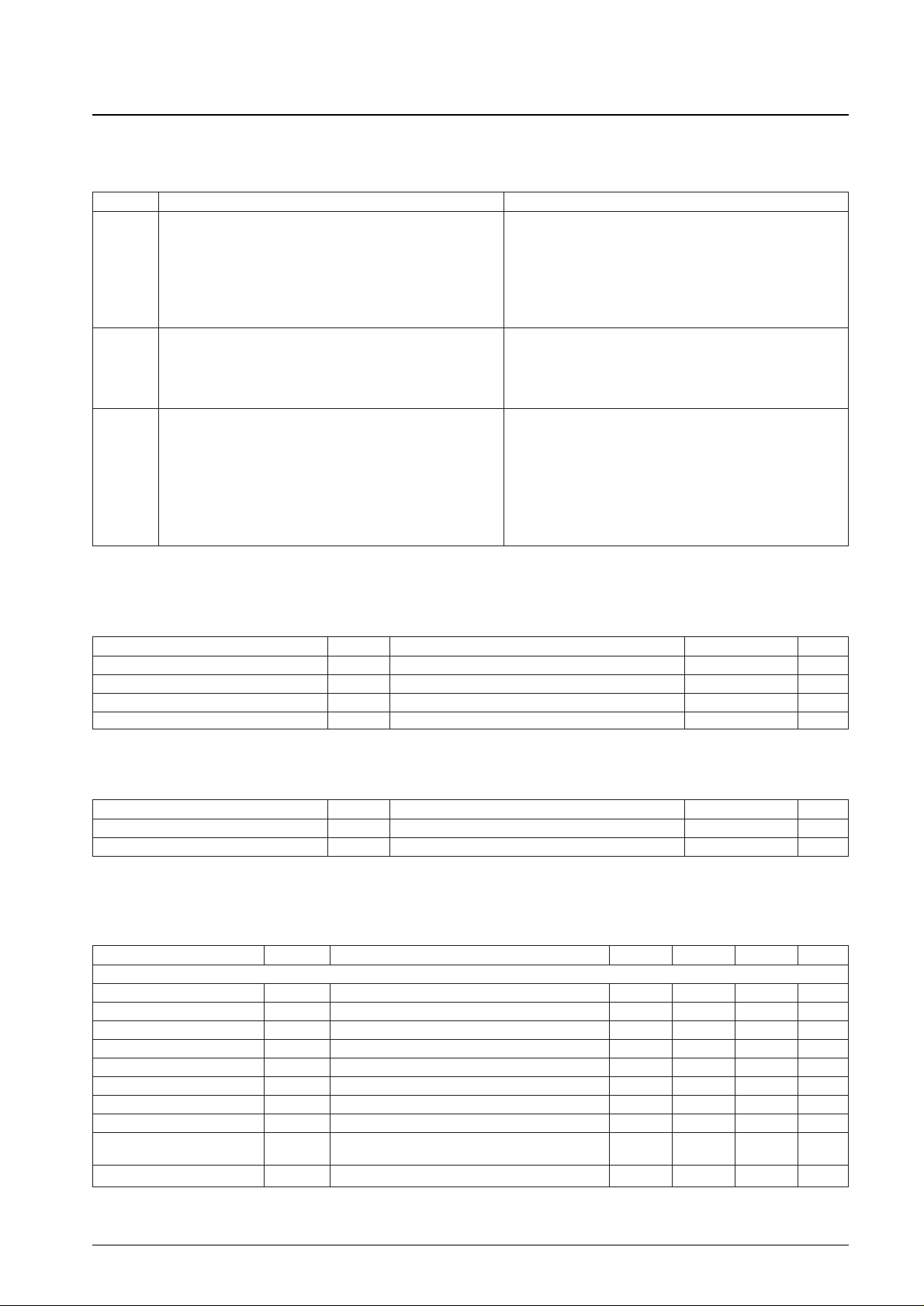
Maximum Ratings at Ta = 25°C
Note: * When mounted on a 70 mm by 65 mm, 1.5 mm thickness Bakelite board. The value for the DIP package is 1150 mW.
Operating Conditions at Ta = 25°C
Operating Characteristics at Ta = 25°C, VCC= 5.0 V
Luminance Chrominance
Video amp.
4.43 BPF Half H killer
Feed back clamp
ACC amp. BGP generator
Main LPF
ACC det. Killer det.
R/P YNR (AVNS)
Main converter VCO
VCA
1.3 M LPF Phase shifter
Sync separator
VXO/XO Sub converter
4.2 V regulator
Side lock det. 5.06 BPF
3rd lock protector
Video AGC amp. NL emphasis Pre amp. Burst gate amp.
Video AGC det. Main emphasis Burst emphasis (NTSC)
REC Pre LPF White/dark clip Killer
Detail enhancer FM modulator APC det.
1/2 f
H
carrier shift AFC det.
FM AGC amp. Drop out det. Pre amp. APC det.
FM AGC det. NL de-emphasis Burst de-emphasis (NTSC) ID det.
Double limiter Picture control PB amp. DCC
FM demodulator Y/C mix Killer Trick det.
PB Sub LPF NAP DPLL
Double high pass noise canceller PAL burst sequence
QV/QH/character insert – Compensator
Main de-emphasis Carrier balancer
DOC Burst gate amp.
Parameter Symbol Conditions Ratings Unit
Maximum supply voltage V
CC
max 7.0 V
Allowable power dissipation Pd max Ta ≤ 65°C* 1350* mW
Operating temperature Topr –10 to +65 °C
Storage temperature Tstg –40 to +150 °C
Parameter Symbol Conditions Ratings Unit
Recommended supply voltage V
CC
5.0 V
Operating supply voltage V
CC
op 4.8 to 5.5 V
Parameter Symbol Conditions min typ max Unit
[Record Mode Y System]
Record mode current drain I
CCR
Input: 1.0 Vp-p video signal 100 130 160 mA
EE output level 1 V
EE
1 Input: 50 Hz system 1.0 Vp-p video signal 2.0 2.1 2.2 Vp-p
AGC characteristics 1 AGC1 Input: 50 Hz system 2.0 Vp-p video signal 2.11 2.21 2.31 Vp-p
AGC characteristics 2 AGC2 Input: 50 Hz system 0.5 Vp-p video signal 1.99 2.09 2.19 Vp-p
AGC characteristics 3 AGC3 Input: 50 Hz system with only SYNC increased 6 dB 590 660 730 mVp-p
AGC characteristics 4 AGC4 Input: 50 Hz system with only SYNC decreased 6 dB 340 380 420 mVp-p
Sync separator output level V
SYR
The SYNC-OUT output pulse wave height 3.9 4.2 4.5 V
Sync separator output pulse width PW
SYR
The SYNC-OUT output pulse width 3.9 4.2 4.6 µs
Sync separator output
∆T
SYR
The SYNC-OUT delay time 0.9 1.1 1.3 µs
prerecord delay time
Sync separator threshold level TH
SYR
–20 –15 dB
Continued on next page.
Page 3
No. 5473-3/8
LA7437, 7437A
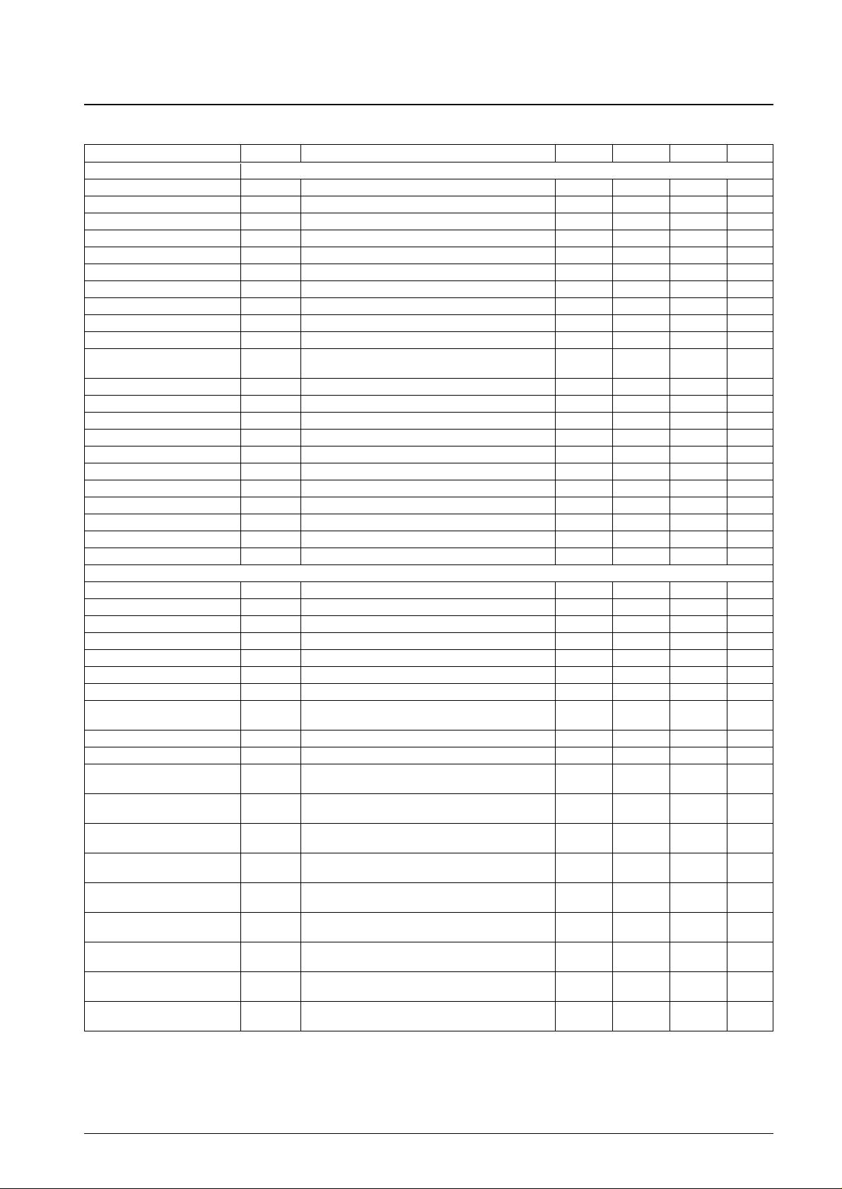
Parameter Symbol Conditions min typ max Unit
[Record Mode Y System]
Pseudo-H insertion level ∆HD
R
With 2.7 V applied to T19A –300 –200 –100 mV
White insertion level ∆WH
R
With 1.3 V applied to T19A 150 300 450 mV
VCA detection voltage V
VCA
2.95 3.10 3.25 V
Record YNR operation EP/LP V
R-YNR1
Input: 50 Hz system standard color bar signal 10 12 14 mVp-p
Y-LPF frequency characteristics 1 YLPF1 The 1 MHz attenuation with respect to 500 kHz –0.5 0.0 +0.5 dB
Y-LPF frequency characteristics 2 YLPF2 The 2 MHz attenuation with respect to 500 kHz –1.0 0.0 +1.0 dB
Y-LPF frequency characteristics 3 YLPF3 The 3.25 MHz attenuation with respect to 500 kHz –6 –4 –2 dB
Y-LPF frequency characteristics 4 YLPF4 The 4.43 MHz attenuation with respect to 500 kHz –33 –25 dB
FM modulator output level V
FM
No input 1.0 1.2 1.4 Vp-p
Carrier frequency 1 F
FM1
50 Hz system 3.7 3.8 3.9 MHz
FM modulator output 2nd
H
MOD
–40 –35 dB
harmonic distortion
Deviation 1 DEV1 50 Hz system 0.95 1.00 1.05 MHz
FM modulator linearity L
MOD
–2 0 2 %
1/2 f
H
carrier shift CS 6.5 7.8 9.1 kHz
Emphasis gain G
EMP
Input: 0.5 Vp-p, 10 kHz sine wave –0.5 0.0 0.5 dB
NL emphasis characteristics 1 G
NLEMP1
Input: 500 mVp-p, 2 MHz sine wave 0.5 1.4 2.3 dB
NL emphasis characteristics 2 G
NLEMP2
Input: 158 mVp-p, 2 MHz sine wave 2.6 3.8 5.2 dB
NL emphasis characteristics 3 G
NLEMP3
Input: 50 mVp-p, 2 MHz sine wave 4.9 6.4 7.9 dB
Main emphases characteristics 1 G
ME1
Input: 100 mVp-p, 500 kHz sine wave 4.9 5.2 5.5 dB
Main emphases characteristics 2 G
ME2
Input: 100 mVp-p, 2 MHz sine wave 13.1 13.6 14.1 dB
White clipping level L
WC
Input: 1.0 Vp-p, white 100% video signal 176 185 194 %
Dark clipping level L
DC
Input: 1.0 Vp-p, white 100% video signal –55 –50 –45 %
[Playback Mode Y System]
Playback mode current drain I
CCP
135 160 185 mA
Dropout compensation time T
DOC
0.72 0.85 0.98 ms
DOC loop gain G
DOC
5H later –1.0 0.0 +1.0 dB
Playback Y level V
VOUT
For playback of an FM signal with a 1.0 MHz deviation 2.0 2.1 2.2 Vp-p
FM demodulator linearity L
DEM
2, 4, 6 MHz –3.5 0.0 +3.5 %
Demodulation sensitivity S
DEM
0.43 0.48 0.53 V/MHz
Carrier leakage CL Input: 4 MHz, 600 mVp-p –40 –35 dB
Playback YNR characteristics
G
P-YNR1
Input: 50% white + CW –2.5 –3.0 –3.5 dB
LP/EP
NL de-emphasis characteristics 1 G
NLDE1
Input: 158 mVp-p, 2 MHz sine wave –6.0 –5.0 –4.0 dB
NL de-emphasis characteristics 2 G
NLDE2
Input: 50 mVp-p, 2 MHz sine wave –10.5 –9.0 –7.5 dB
Double noise canceller
G
WNC1
Input: 158 mVp-p, 2 MHz sine wave –1.8 –1.3 –0.8 dB
characteristics 1
Double noise canceller
G
WNC2
Input: 50 mVp-p, 2 MHz sine wave –6.2 –5.2 –4.2 dB
characteristics 2
Double noise canceller
G
WNC3
Input: 15.8 mVp-p, 2 MHz sine wave –11.7 –10.7 –8.7 dB
characteristics 3
PIC-CTL hard response
G
PH1
Input: 50% video + sine wave f = 1 MHz, 158 mVp-p 4.0 5.0 6.0 dB
characteristics 1
PIC-CTL hard response
G
PH2
Input: 50% video + sine wave f = 2 MHz, 158 mVp-p 6.5 7.5 8.5 dB
characteristics 2
PIC-CTL soft response
G
PS1
Input: 50% video + sine wave f = 1 MHz, 158 mVp-p –4.5 –3.5 –2.5 dB
characteristics 1
PIC-CTL soft response
G
PS2
Input: 50% video + sine wave f = 2 MHz, 158 mVp-p –9.0 –7.0 –5.0 dB
characteristics 2
Pseudo-V insertion level
∆VD
P
With 5 V applied to T19A –150 –50 +50 mV
(playback)
Pseudo-H insertion level
∆HD
P
With 2.7 V applied to T19A –300 –200 –100 mV
(playback)
Continued on next page.
Continued from preceding page.
Page 4
No. 5473-4/8
LA7437, 7437A
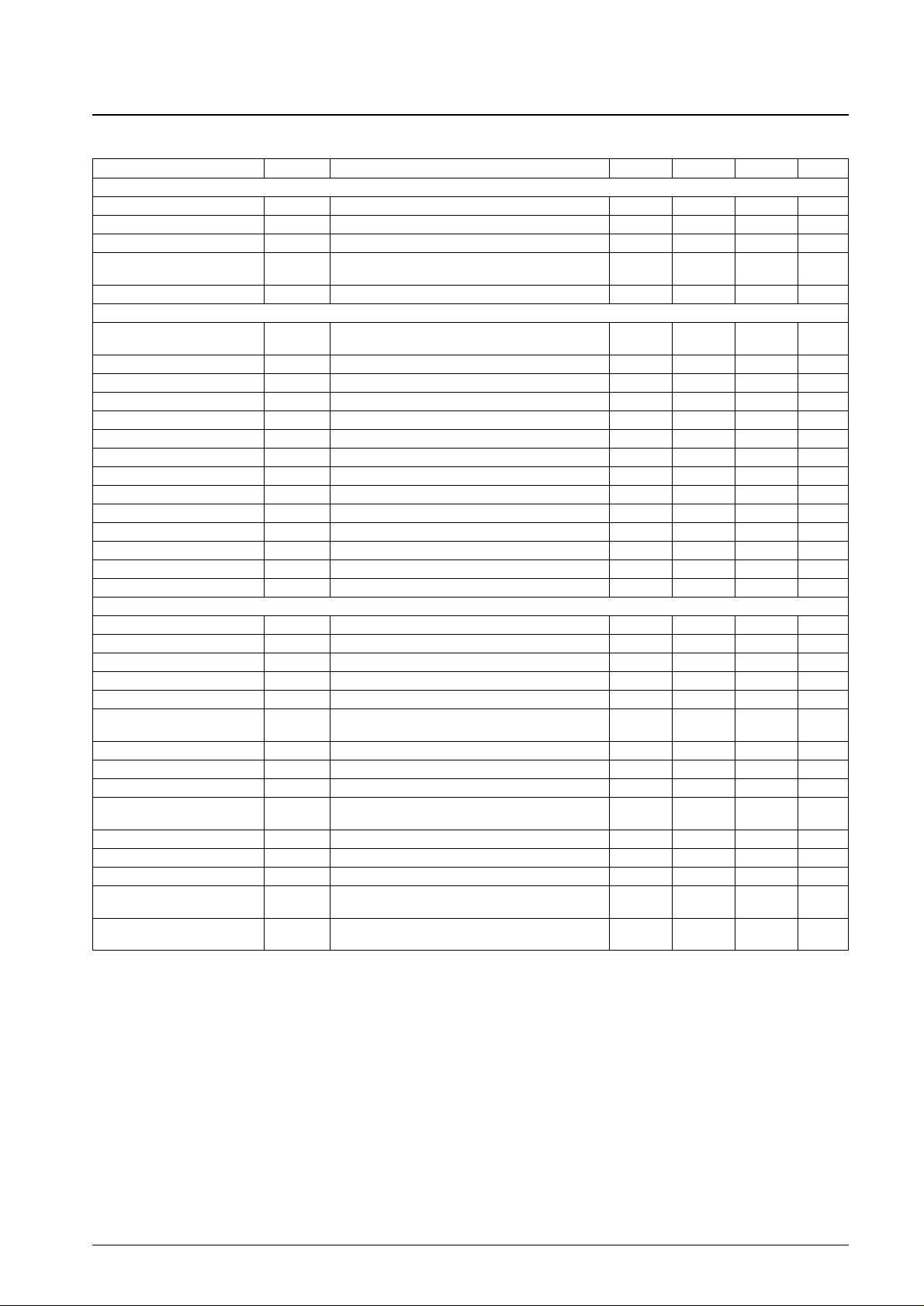
Parameter Symbol Conditions min typ max Unit
[Record Mode Y System]
White insertion level (playback) ∆WH
P
With 1.3 V applied to T14A 150 300 450 mV
Sync separator output level V
SYP
The SYNC-OUT output pulse wave height 3.9 4.2 4.5 V
Sync separator output pulse width PW
SYP
The SYNC-OUT output pulse width 4.2 4.5 4.8 µs
Sync separator output
∆T
SYP
1.4 1.6 1.8 µs
pre-record delay time
4.2 V regulator voltage V
REG
4.0 4.2 4.4 V
[Record Mode Chrominance System]
Chrominance low band
V
OR-38
Input: PAL/GBI standard color bar signal, 1 Vp-p 150 190 230 mVp-p
conversion output burst level
VXO oscillator level 1 V
VXO-R1
Input: PAL/GBI standard color bar signal, 1 Vp-p 300 500 700 mVp-p
Record ACC characteristics 1 ACC
-R1
With only the chrominance signal level increased 6 dB +0.2 +0.6 dB
Record ACC characteristics 2 ACC
-R2
With only the chrominance signal level decreased 6 dB –0.5 –0.1 dB
ACC killer on input level V
ACCK-ON
–26 dB
ACC killer on output level V
O-ACCK
–60 –50 dB
ACC killer recovery input level V
ACCK-OFF
–20 dB
VXO control sensitivity S
VXO
3.8 5.7 7.6 Hz/m
APC pull-in range 1 ∆f
APC1
350 Hz
APC pull-in range 2 ∆f
APC2
–350 Hz
BGP delay time t
D
Input: PAL/GBI standard color bar signal, 1 Vp-p 3.1 3.4 3.7 µs
BGP pulse width t
W
4.7 4.9 5.1 µs
AFC pull-in range 1 ∆f
AFC1
+1.0 +7.0 kHz
AFC pull-in range 2 ∆f
AFC2
–3.7 –1.0 kHz
[Playback Mode Chrominance System]
Video output burst level V
OP-11
SP mode, input: burst 30 mVp-p 255 300 345 mVp-p
Pin 25 output burst level V
OP-25
SP mode, input: burst 30 mVp-p 195 230 265 mVp-p
Playback ACC characteristics 1 ACC
-P1
With the chrominance level increased 6 dB +0.5 +0.8 dB
Playback ACC characteristics 2 ACC
-P2
With the chrominance level decreased 6 dB –0.8 –0.5 dB
Playback killer on input level V
ACK-P
–40 –32 –25 dB
Playback killer on chrominance
V
OACK-P
–44 –40 dB
output level
Main converter carrier leakage C
LP
The 5.06 MHz carrier leakage component –40 –33 dB
Burst de-emphasis level NT G
BD
NTSC mode –5.25 –5.0 –4.75 dB
Playback XO output level 1 V
XO-P1
300 450 600 mVp-p
Playback XO oscillator
∆f
XO
∆fXO = f – 4.43361875 (MHz) –9 0 +9 Hz
frequency deviation
SLD detector current 1 I
SLD1
135 µA
SLD detector current 2 I
SLD2
135 µA
NTSC playback burst output level V
BNT
NTSC mode 255 300 345 mVp-p
NTSC to PAL conversion -
VB-NAP –1.0 0.0 +1.0 dB
V axis burst level
NTSC to PAL conversion burst
∆B-NAP –2.0 0.0 +2.0 dB
level ratio
Continued on next page.
Continued from preceding page.
Page 5
No. 5473-5/8
LA7437, 7437A
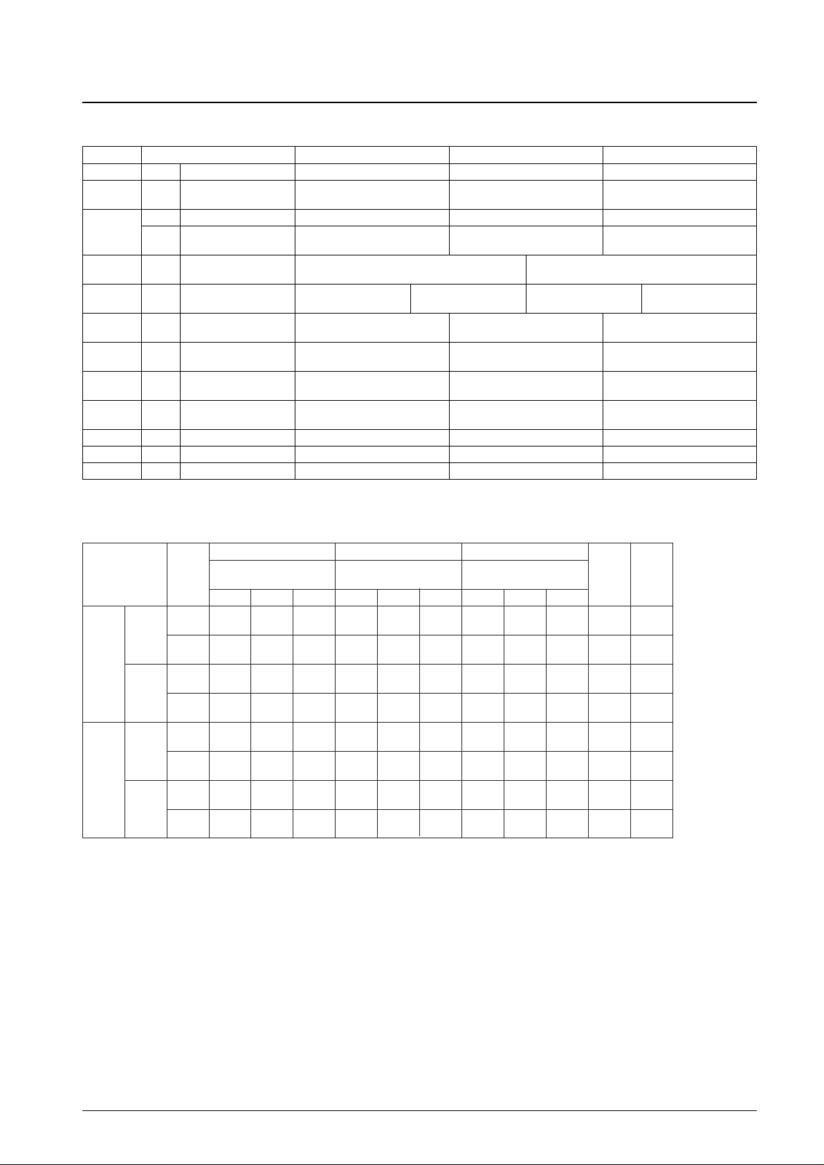
LA7437A Control Pin Table
Note: Do not allow pin 3 to fall under 1.5 V. (The chip will enter test mode.)
Function Control in each of the LA7437A Operating Modes
Note: 1. K1 is the YNR coefficient, K2 is the LNC coefficient
2. Use the 1/2 f
H
carrier shift entries in parentheses when pin 23 is high.
3. The detail enhancer is off when pin 18 is at the middle level.
Pin No. Control function L M H
9 R/P Edit 3.8 VDC or more
40 R/P YNR (AVNS)-CTL
1.0 VDC to less 1.5 to 2.5 VDC 3.5 VDC or more
YNR-off YNR-CTL YNR (strong)
R ****** 3.9 VDC or more
11
P N, C, CTL
1.5 VDC or less 2.0 to 3.0 VDC
N, C-off N, C-CTL
17 R/P C-rotary
0 to 1.9 VDC 2.3 VDC or more
Low CH High CH
19 P QV/QH CHARA. INS
0.8 VDC or less 1.2 to 2.2 VDC 2.6 to 3.3 VDC 3.7 VDC or more
Through CHARA insert Pedestal insert QV insert
25 R/P EP/LP/SP
1.2 VDC or less 2.0 to 2.7 VDC 3.9 VDC or more
SP LP EP
28 R SP carrier shift stop
3.0 VDC or more
SP carrier shift stop
27 P NAP
1.2 VDC or less 2.0 to 2.7 VDC 3.3 VDC or more
Through Balanced-mod output NAP-on
30 R/P NT/MESEC/PAL
1.2 VDC or less 2.0 to 2.7 VDC 3.9 VDC or more
PAL MESEC NTSC
33 P Trick 3.9 VDC or more
2 P DOC-off 4.1 VDC or more
6 R/P PB-H 4.0 VDC or more
YNR Detail enhancer NC
1/2 f
H
Edit Pin 40 control Pin 11 control Pin 11 control PIC-CTL carrier
shift
L M H L M H L M H
On Off Off Off Off Variable Center — — — —
●●
SP
(
✕)
Off Off Off Off Off Variable Center — — — —
●●
REC
(✕)
On Off
K1 = 0.2 K1 = 0.2
Off Variable Center — — — — ●●
LP
K2 = 0.0 K2 = 0.0
EP
Off Off
K1 = 0.5 K1 = 0.5
Off Variable Center — — — — ●●
K2 = 0.0 K2 = 0.0
On
K1 = 0.0 K1 = 0.0 K1 = 0.5
— — — Off Variable Center Center —
SP
K2 = 0.0 K2 = 0.0 K2 = 0.0
Off
K1 = 0.0 K1 = 0.2 K1 = 0.5
— — — Off Variable Center ●● —
PB
K2 = 0.0 K2 = 0.0 K2 = 0.0
On
K1 = 0.0 K1 = 0.2 K1 = 0.5
— — — Off Variable Center Center —
LP
K2 = 0.5 K2 = 0.5 K2 = 0.5
EP
Off
K1 = 0.0 K1 = 0.2 K1 = 0.5
— — — Off Variable Center ●● —
K2 = 0.5 K2 = 0.5 K2 = 0.5
Page 6
No. 5473-6/8
LA7437, 7437A
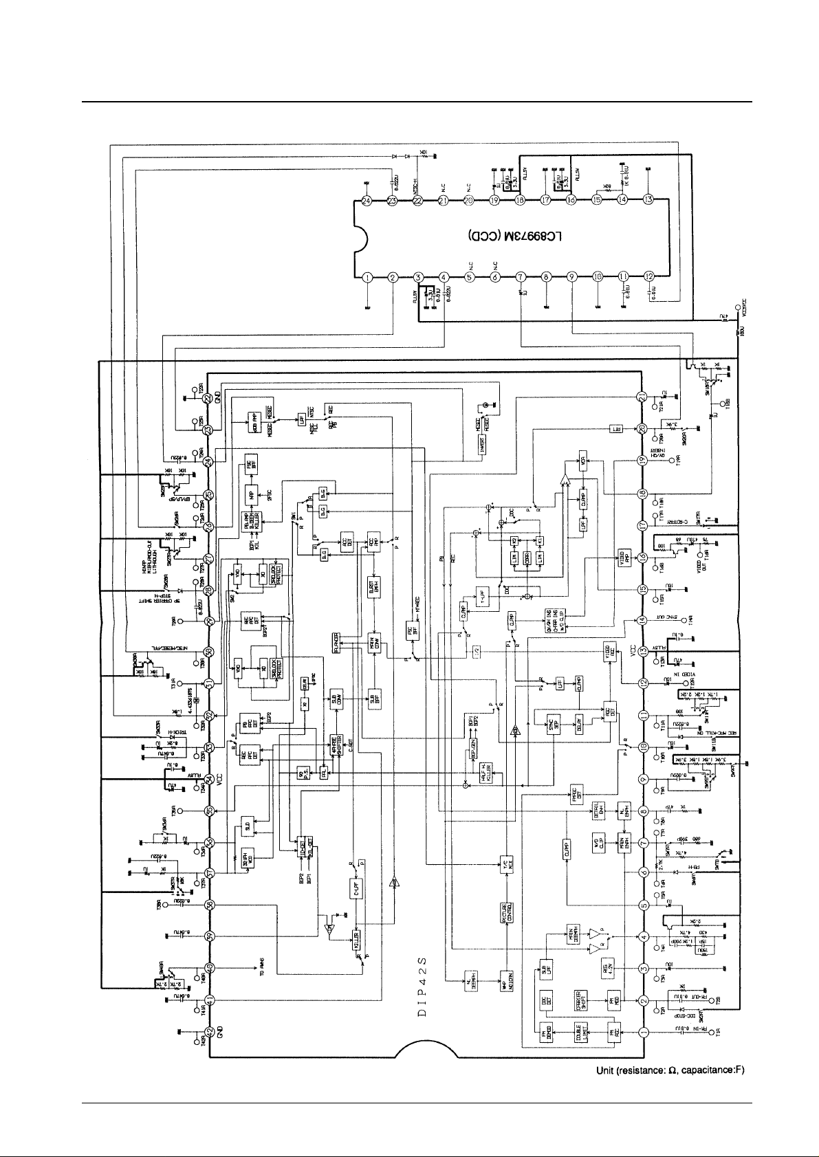
LA7437 Test Circuit
Page 7
No. 5473-7/8
LA7437, 7437A
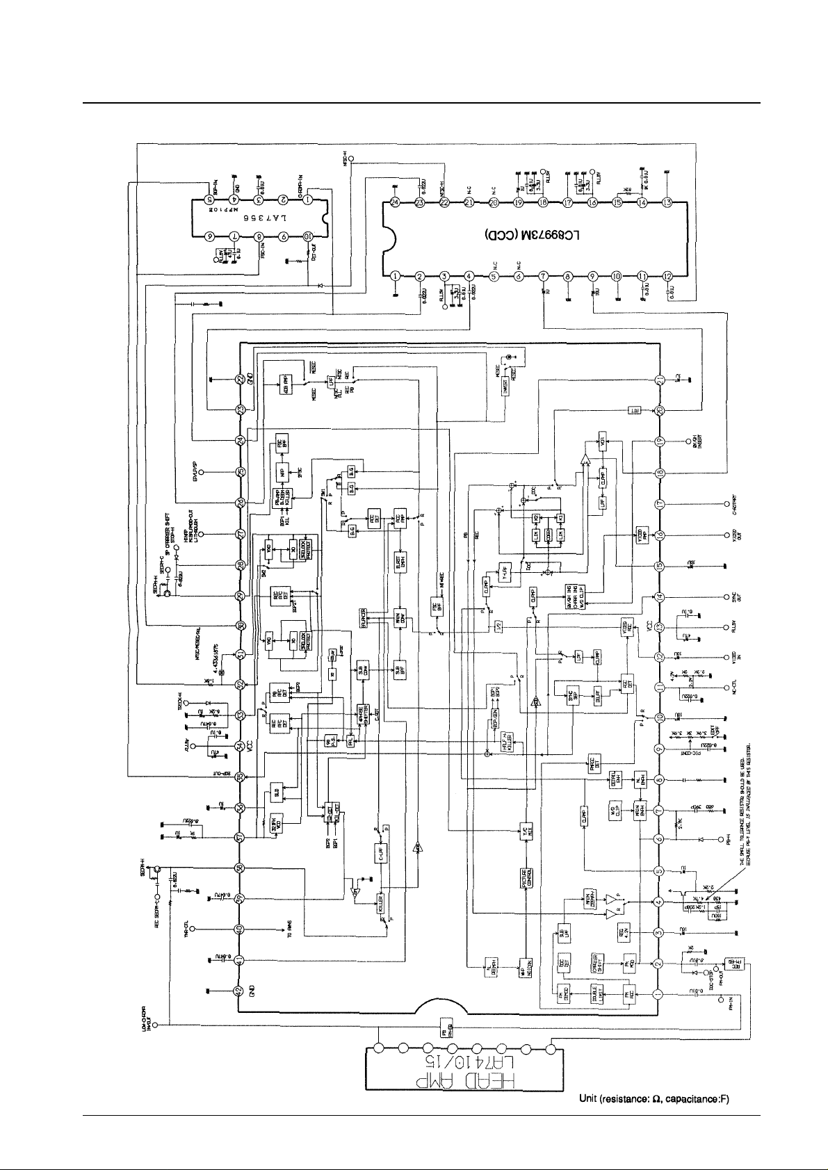
LA7437 Block Diagram
Page 8

No. 5473-8/8
LA7437, 7437A
This catalog provides information as of December, 1997. Specifications and information herein are subject to
change without notice.
■ No products described or contained herein are intended for use in surgical implants, life-support systems, aerospace
equipment, nuclear power control systems, vehicles, disaster/crime-prevention equipment and the like, the failure of
which may directly or indirectly cause injury, death or property loss.
■ Anyone purchasing any products described or contained herein for an above-mentioned use shall:
➀ Accept full responsibility and indemnify and defend SANYO ELECTRIC CO., LTD., its affiliates, subsidiaries and
distributors and all their officers and employees, jointly and severally, against any and all claims and litigation and all
damages, cost and expenses associated with such use:
➁ Not impose any responsibility for any fault or negligence which may be cited in any such claim or litigation on
SANYO ELECTRIC CO., LTD., its affiliates, subsidiaries and distributors or any of their officers and employees
jointly or severally.
■ Information (including circuit diagrams and circuit parameters) herein is for example only; it is not guaranteed for
volume production. SANYO believes information herein is accurate and reliable, but no guarantees are made or implied
regarding its use or any infringements of intellectual property rights or other rights of third parties.
 Loading...