

Page 1
Monolithic Linear IC
No. 5647
VHS VCR Playback Head and Record Amplifiers
Overview
The LA7415 is a record and playback amplifier IC for
VHS format VCR decks. In combination with a Sanyo
LC7420 or LA7430 Series video signal processing IC, the
LA7415 can provide an adjustment-free Y/C record
current.
Features
• Record amplifier: Provides stable recording
characteristics using a fixed-current drive technique that
is resistant to load variations.
• REC-AMP: Includes a built-in AGC circuit.
• Can use the same printed circuit board as the LA7411.
LA7415
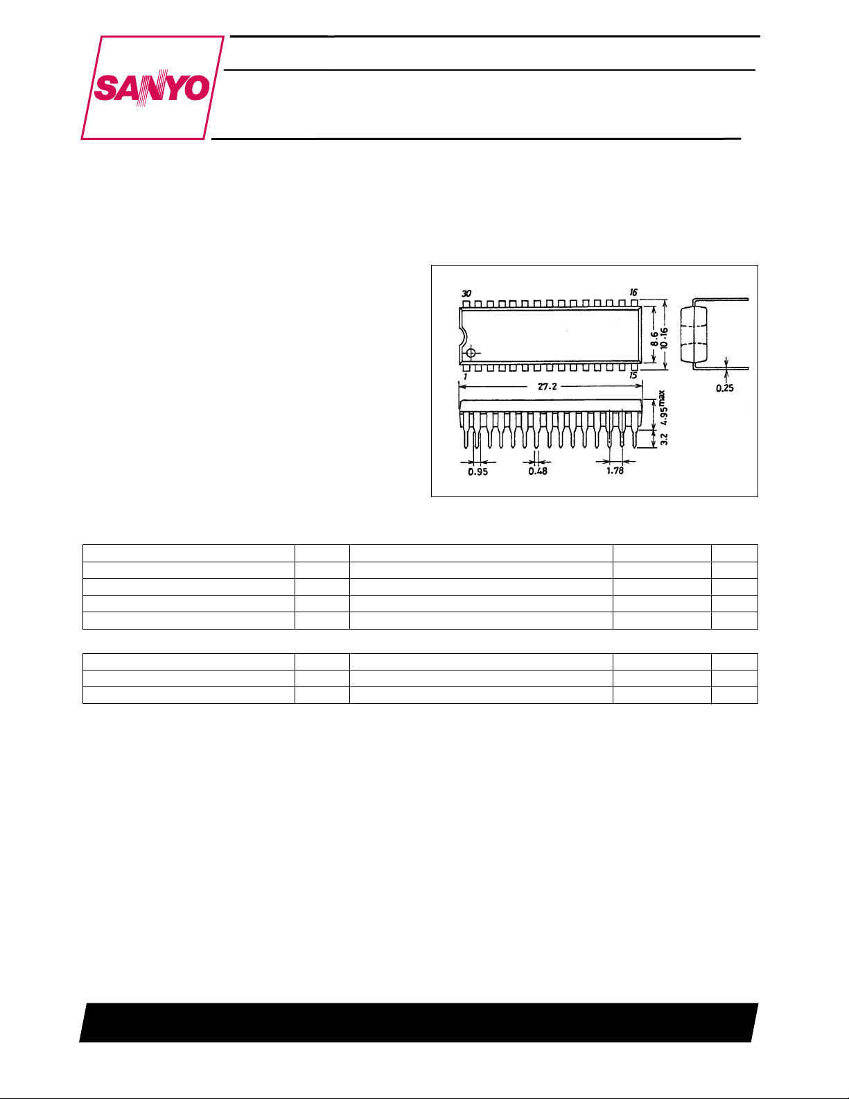
Package Dimension
unit: mm
3061-DIP30S
[LA7415]
SANYO: DIP30S
Specifications
Maximum Ratings at Ta = 25°C
Parameter Symbol Conditions Ratings Unit
Maximum supply voltage V
Allowable power dissipation Pd max Ta ≤ 65 °C 650 W
Operating temperature Topr –10 to +65 °C
Storage temperature Tstg –40 to +150 °C
Operating Conditions at Ta = 25°C
Parameter Symbol Conditions Ratings Unit
Supply voltage V
Operating voltage range V
max 7.0 V
CC
CC
op 4.8 to 5.5 V
CC
5.0 V
SANYO Electric Co.,Ltd. Semiconductor Bussiness Headquarters
TOKYO OFFICE Tokyo Bldg., 1-10, 1 Chome, Ueno, Taito-ku, TOKYO, 110 JAPAN
43097HA(OA) No. 5647-1/12
Page 2
LA7415
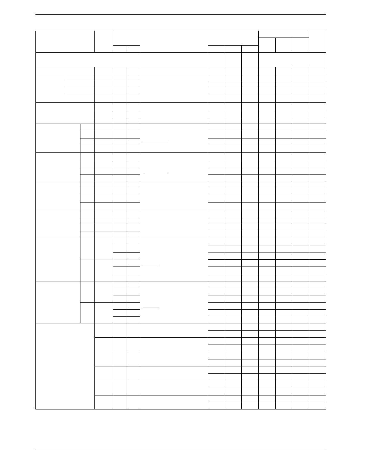
Electrical Characteristics at Ta = 25°C
Ratings
Parameter Symbol Conditions
Input Output T2 T4 T5
[Playback Mode]
Current drain I
SP L CH1 VG
Voltage gain
SP H CH2 VG
EP L CH3 VG
EP H CH4 VG
Voltage gain differential 1 ∆VG
Voltage gain differential 2 ∆VG
Inter-mode gain difference ∆
Equivalent input CH2 V
noise voltage CH3 V
CH1 V
CH4 V
CCP
1 T20A T10A OPEN 0 0 54.0 57.0 60.0 dB
P
2 T23A T10A
P
3 T27A T10A
P
4 T30A T10A OPEN 5.0 2.5 56.0 59.0 62.0 dB
P
1– –VGP1 – VGP2––––10+1dB
P
2– –VGP3 – VGP4––––10+1dB
P
VG
NIN
NIN
NIN
NIN
––VGP3 – VGP1–––123dB
P EP-SP
1 T20A T10A
2 T23A T10A
3 T27A T10A
4 T30A T10A OPEN 5.0 2.5 – 1.1 1.5 µVrms
CH1 ∆Vfp1 T20A T10A
Frequency CH2 ∆Vfp2 T23A T10A
characteristics CH3 ∆Vfp3 T27A T10A
CH4 ∆Vfp4 T30A T10A
CH1 V
Second harmonic CH2 V
distortion CH3 V
CH4 V
CH1 V
Maximum CH2 V
output level CH3 V
CH4 V
1 T20A T10A
HDP
2 T23A T10A
HDP
3 T27A T10A
HDP
4 T30A T10A
HDP
1 T20A T10A
OMP
2 T23A T10A
OMP
3 T27A T10A
OMP
4 T30A T10A OPEN 5.0 2.5 1.0 1.2 – Vp-p
OMP
T15: 5.0 V, T13: OPEN, TRCK HA SW30
T7: OPEN MUTE
Pin 15 influx current OPEN 0 0 24 30 36 mA
= 38 mVp-p,
V
IN
f = 1 MHz
After the 1.1-MHz LPF
V
OUT
VG
1, 2, 3, 4
P
V
= 38 mVp-p
IN
f = 7 MHz
V
OUT
1, 2, 3, 4 output ratio
VG
P
V
= 38 mVp-p
IN
f = 4 MHz
(8-MHz component)/(4-MHz component)
output ratio
f = 1 MHz
The output level when the third
harmonic in the output is –30 dB
OPEN 0 2.5 54.0 57.0 60.0 dB
OPEN 5.0 0 56.0 59.0 62.0 dB
OPEN 0 0 – 1.1 1.5 µVrms
OPEN 0 2.5 – 1.1 1.5 µVrms
OPEN 5.0 0 – 1.1 1.5 µVrms
OPEN 0 0 –2.5 0 – dB
OPEN 0 2.5 –2.5 0 – dB
OPEN 5.0 0 –2.5 0 – dB
OPEN 5.0 2.5 –2.5 0 – dB
OPEN 0 0 – –40 –35 dB
OPEN 0 2.5 – –40 –35 dB
OPEN 5.0 0 – –40 –35 dB
OPEN 5.0 2.5 – –40 –35 dB
OPEN 0 0 1.0 1.2 – Vp-p
OPEN 0 2.5 1.0 1.2 – Vp-p
OPEN 5.0 0 1.0 1.2 – Vp-p
T23A T10A OPEN 0 0 – –40 –35 dB
CH1 V
Crosstalk SP T30A T10A
(Note 1) T20A T10A
CH2 V
1 T27A T10A
CR
2 T27A T10A
CR
V
= 38 mVp-p,
IN
f = 4 MHz
V
OUT
1, 2
VG
P
OPEN 0 0 – –40 –35 dB
OPEN 0 0 – –40 –35 dB
OPEN 0 2.5 – –40 –35 dB
OPEN 0 2.5 – –40 –35 dB
T30A T10A OPEN 0 2.5 – –40 –35 dB
T23A T10A OPEN 5.0 0 – –40 –35 dB
CH3 V
Crosstalk EP T30A T10A
(Note 1) T20A T10A
CH4 V
3 T27A T10A
CR
4 T27A T10A
CR
V
= 38 mVp-p,
I
f = 4 MHz
V
OUT
3, 4
VG
P
OPEN 5.0 0 – –40 –35 dB
OPEN 5.0 0 – –40 –35 dB
OPEN 5.0 2.5 – –40 –35 dB
OPEN 5.0 2.5 – –40 –35 dB
T30A T10A OPEN 5.0 2.5 – –40 –35 dB
∆V
1 – T10 CH1-CH2
ODC
∆V
2 – T10 CH3-CH4
ODC
∆V
3 – T10 CH1-CH3
Output DC OPEN 5.0 0 –100 0 +100 mV
offset
ODC
∆V
4 – T10 CH2-CH4
ODC
∆V
5 – T10 CH1-CH4
ODC
∆V
6 – T10 CH2-CH3
ODC
OPEN – 0 –100 0 +100 mV
OPEN 0 2.5 –100 0 +100 mV
OPEN – 0 –100 0 +100 mV
OPEN 5.0 2.5 –100 0 +100 mV
OPEN 0 – –100 0 +100 mV
OPEN 0 – –100 0 +100 mV
OPEN 5.0 2.5 –100 0 +100 mV
OPEN 0 0 –100 0 +100 mV
OPEN 5.0 2.5 –100 0 +100 mV
OPEN 0 2.5 –100 0 +100 mV
OPEN 5.0 0 –100 0 +100 mV
Note 1. With the input inductor L (8.2 µH) shorted.
Since the T4 (HA) control switch timing is synchronized with T6 (H-Sync), a T6 trigger (0 - 5 V - 0) must be input before measuring each of these items.
2.
min typ max
Continued on the next page.
Unit
No. 5647-2/12
Page 3
LA7415
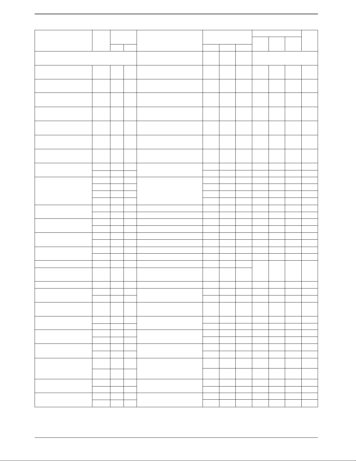
Continued from the preceding page.
Parameter Symbol Conditions
Input Output T2 T4 T5
T15: 5.0 V, T13: OPEN, TRCK HA SW30
T7: OPEN MUTE
Enveloped detector
output pin voltage
Enveloped detector
voltage SP1 T10A: Adjusted to 300 mV p-p
Enveloped detector
voltage SP2 T10A: Adjusted to 600 mV p-p
Enveloped detector
voltage EP1 T10A: Adjusted to 200 mV p-p
Enveloped detector
voltage EP2 T10A: Adjusted to 450 mV p-p
Comparator
output voltage 1 The T3 DC voltage
Comparator
output voltage 2 The T3 DC voltage
Playback mode on switching
transistor on resistance
Playback mode
mode switching
transistor on
resistance
Trick 1 threshold
level
Trick 2 threshold
level
HAPB threshold
level
SW30 threshold
level
[Record Mode]
Current drain I
AGC amplifier
output level
Inter-mode gain
difference
AGC amplifier control
characteristics 1
AGC amplifier control
characteristics 2
AGC amplifier frequency
characteristics
AGC amplifier second
harmonic distortion
AGC amplifier maximum
output level
AGC amplifier muting
attenuation
V
ENV
V
ENVSP1
V
ENVSP2
V
ENVEP1
V
ENVEP2
V
COMP1
V
COMP2
R
17 P-17
PON
18 P-18
R
PON
21 P-21 OPEN 5.0 – – 4.0 6.0 Ω
R
PON
R
24 P-24
PON
26 P-26
R
PON
29 P-29 OPEN 0 – – 4.0 6.0 Ω
R
PON
T8 The T8 DC voltage with no input OPEN 0 0 0 0.4 0.8 V
T20A T8
T20A T8
T27A T8
T27A T8
T20A T3
T20A T3
f = 4 MHz
f = 4 MHz
f = 4 MHz
f = 4 MHz
f = 4 MHz, V
f = 4 MHz, V
= 38 mVp-p
IN
= 38 mVp-p
IN
The difference in the DC measurement
for 1-mA and 2-mA influx currents
The difference in the DC measurement
for 1-mA and 2-mA influx currents
TR1-1 T2 Normal → Trick1 * – – 3.2 – 5.0 V
TR1-2 T2 Trick1 → Normal * – – 1.2 – 2.8 V
TR2-1 T2 Normal → Trick2 * – – 0.0 – 0.8 V
TR2-2 T2 Trick2 → Normal * – – 1.2 – 2.8 V
HAP-1 T4 SP → EP – * – 1.8 – 5.0 V
HAP-2 T4 EP → SP – * – 0.0 – 1.4 V
SW30-1 T5 Lch → Hch – – * 1.2 – 5.0 V
SW30-2 T4 Hch → Lch – – * 0.0 – 0.8 V
T15: 5.0 V, T2: OPEN, REC HA SW30
T6: 5.0 V, T7: 5.0 V Adj2 MUTE
The pin 15 influx current OPEN 0 0 44 55 66 mA
f = 4 MHz
V
= 200 mVp-p
IN
RSP/VREP
f = 4 MHz, V
The output level/V
f = 4 MHz, V
The output level/V
f = 1 MHz, 7 MHz, VIN= 100 mVp-p
The 7 MHz/1 MHz output ratio
f = 4 MHz, V
= 400 mVp-p
IN
RSP, EP
= 100 mVp-p
IN
RSP, EP
= 200 mVp-p
IN
The (8 MHz component)/(4 MHz component)
output ratio
f = 4 MHz, The output level for which
the second harmonic is –35 dB
f = 4 MHz, VI = 200 mVp-p
The output level/V
RSP, EP
∆
∆
∆
∆
∆V
∆V
∆V
∆V
V
V
∆VG
V
AGC
V
AGC
V
AGC
V
AGC
∆V
∆V
∆V
∆V
CCR
RSP
REP
FRS
FRE
HDRS
HDRE
OMRS
OMRE
MRS
MRE
T11A T21A
T11A T26A
––V
R
1-SP
T11A T21A
1-EP
T11A T26A
2-SP
T11A T21A
2-EP
T11A T26A
T11A T21A
T11A T26A
T11A T21A
T11A T21A
T11A T21A
T11A T26A
T11A T21A
T11A T26A
ratio
ratio
ratio
Ratings
min typ max
Unit
OPEN 0 0 2.1 2.6 3.1 V
OPEN 0 0 4.5 4.8 5.0 V
OPEN 5.0 0 2.0 2.6 3.0 V
OPEN 5.0 0 4.5 4.8 5.0 V
5.0 0 0 – 0.4 0.7 V
5.0 5.0 0 4.5 4.8 – V
– – – – 4.0 6.0 Ω
– – – – 4.0 6.0 Ω
OPEN 5.0 – – 4.0 6.0 Ω
OPEN 0 – – 4.0 6.0 Ω
T2 T4 T5
OPEN 0 0 147 156 165 mVp-p
OPEN 5.0 0 116 123 130 mVp-p
– – – 1.30 2.05 2.80 dB
OPEN 0 0 – 0.5 1.0 dB
OPEN 5.0 0 – 0.5 1.0 dB
OPEN 0 0 –1.0 –0.5 – dB
OPEN 5.0 0 –1.0 –0.5 – dB
OPEN 0 0 –1.0 –0.0 +1.0 dB
OPEN 5.0 0 –1.0 –0.0 +1.0 dB
OPEN 0 0 – –45 –40 dB
OPEN 5.0 0 – –45 –40 dB
Adj. 0 0 20 22 – mAp-p
Adj. 5.0 0 20 22 – mAp-p
OPEN 0 5.0 – –45 –40 dB
OPEN 5.0 5.0 – –45 –40 dB
Continued on the next page.
No. 5647-3/12
Page 4
Continued from the preceding page.
Parameter Symbol Conditions
[Record Mode]
LA7415
Input Output T2 T4 T5
T15: 5.0 V, T2: OPEN, REC HA SW30
T6: 5.0 V, T7: 5.0 V Adj2 MUTE
Ratings
min typ max
Unit
AGC amplifier
relative cross
modulation level
Record mode
mode switching
transistor on
resistance
HA record
threshold level
Record MUTE
threshold level
Record/playback
threshold level
Notes 3. Measure with a DC voltage of about 1.8 V applied to the AGC detector filter pin (pin 12) and with the AGC amplifier gain fixed.
4. Adjust the output level by applying a DC voltage to T13 (REC CUR.Adj2)
5. Use a resistor with a ±1.0% tolerance between pins 14 and 15.
∆V
∆V
R
R
R
R
R
R
HAR-1 T4 SP → EP – *–1.8 – 5.0 V
HAR-2 T4 EP → SP – *–0.0 – 1.4 V
MUTE-1 T5 MUTE OFF → ON – – * 3.4 – 5.0 V
MUTE-2 T5 MUTE ON → OFF – – * 0.0 – 3.0 V
SW REC/PB
T10A T21A
CYS
T11A T26A
CYE
17 P-17 OPEN 5.0 – – 4.0 6.0 Ω
RON
18 P-18
RON
21 P-21
RON
24 P-24
RON
26 P-26 OPEN 0 – – 4.0 6.0 Ω
RON
29 P-29 OPEN 0 – – 4.0 6.0 Ω
RON
T10A: f = 629 kHz, VIN= 360 mVp-p
T11A: f = 4 MHz, VIN= 200 mVp-p
(4 MHz ±629 kHz)/(4 MHz)
output ratio
The difference in the DC
measurement for 1-mA
and 2-mA influx currents
T7: control voltage – – – 2.2 – 5.0 V
OPEN 0 0 – –45 –40 dB
OPEN 5.0 0 – –45 –40 dB
OPEN 0 – – 4.0 6.0 Ω
OPEN 5.0 – – 4.0 6.0 Ω
OPEN 5.0 – – 4.0 6.0 Ω
Usage Notes
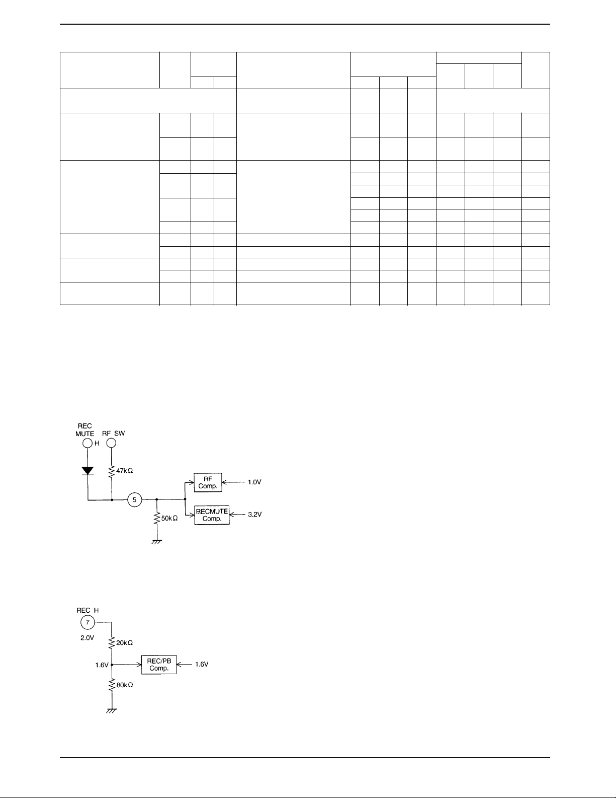
1. Control Pin Logic
RF SW, REC MUTE: pin 5
Record/playback mode switching: pin 7
Playback mode
If the pin 5 DC voltage is < 1.0 V: Lch
If the pin 5 DC voltage is > 1.0 V: Hch
Record mode
If the pin 5 DC voltage is < 3.2 V: Muting will be off
If the pin 5 DC voltage is > 3.2 V: Muting will be on
If the pin 7 DC voltage is < 2.0 V: Playback mode
If the pin 7 DC voltage is > 2.0 V: Record mode
No. 5647-4/12
Page 5
LA7415
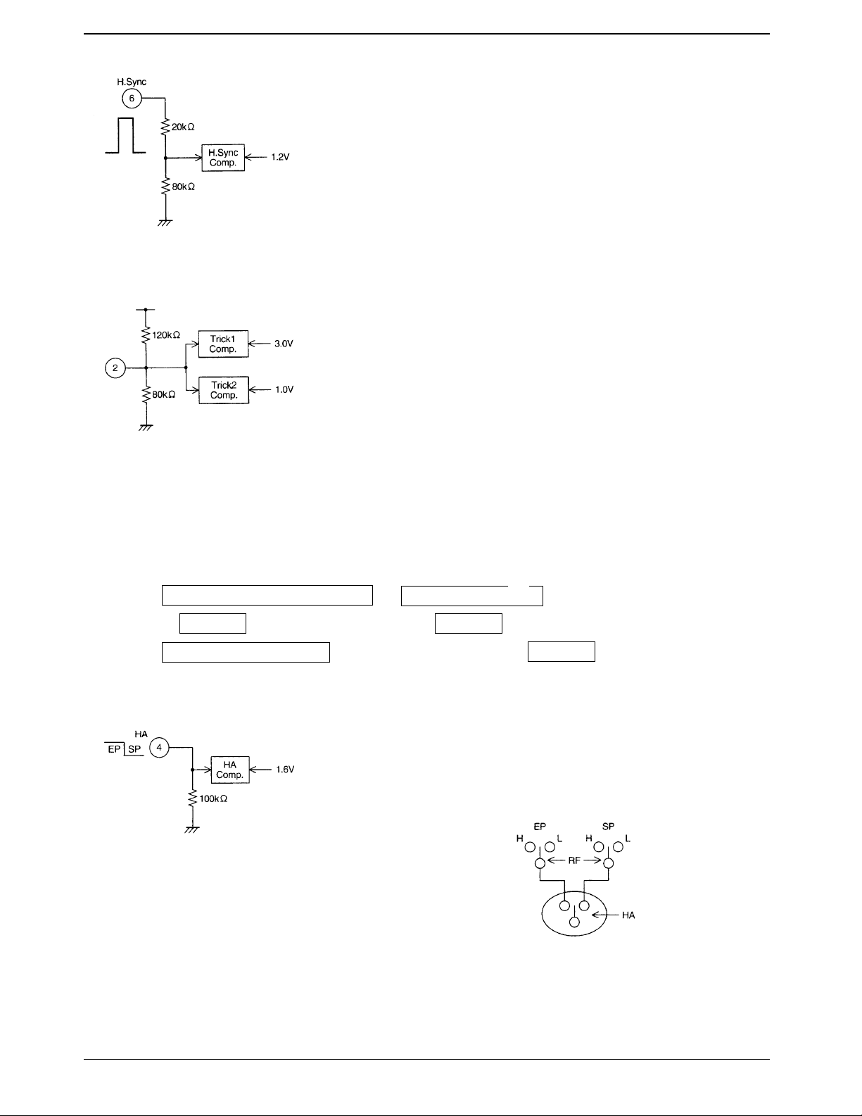
H.Sync input: pin 6
If the pin 6 DC voltage is > 1.5 V: Currently the signal is in an
H.Sync period
*: Playback mode: Used for switching timing in SP search.
Record mode: Used as the record amplifier AGC synchronization block gate pulse.
(4) Playback trick mode switching: pin 2
If the pin 2 DC voltage is > 3.0 V: Trick 1
If the pin 2 DC voltage is < 1.0 V: Trick 2
If the pin 2 DC voltage is > 1.0 V and < 3.0 V: Normal
*: Normal mode: Two channels controlled (EP/SP) by pin 4: ON
Envelope comparator: OFF
In trick 1 and 2 modes: All 4 channels: ON
Envelope comparator: ON
*: The difference between trick 1 and trick 2 is that:
Trick1 →
Trick2 → SP search is performed in the [HA switch] path. (See the block diagram.)
Envelope comparator (pin 3) output
→→SP search is performed in the [HA switch] path.
Pin 4 HA HA switch
Servo (microcontroller)
Envelope comparator output
or
HA switch
HA SW (EP/SP mode switching): pin 4
If the pin 4 DC voltage is < 1.6 V: SP mode
If the pin 4 DC voltage is > 1.6 V: EP mode
*: H.Sync synchronization for HA switching:
The switching of the HA SW circuit show in the figure at the right
is synchronized with the H.Sync signal input to pin 6.
(Other EP/SP switching is performed in real time.)
Comp.OUT (pin 3)
If the EP envelope is > SP: High (4.0 V or higher)
If the EP envelope is < SP: Low (0.7 V or lower)
No. 5647-5/12
Page 6
LA7415
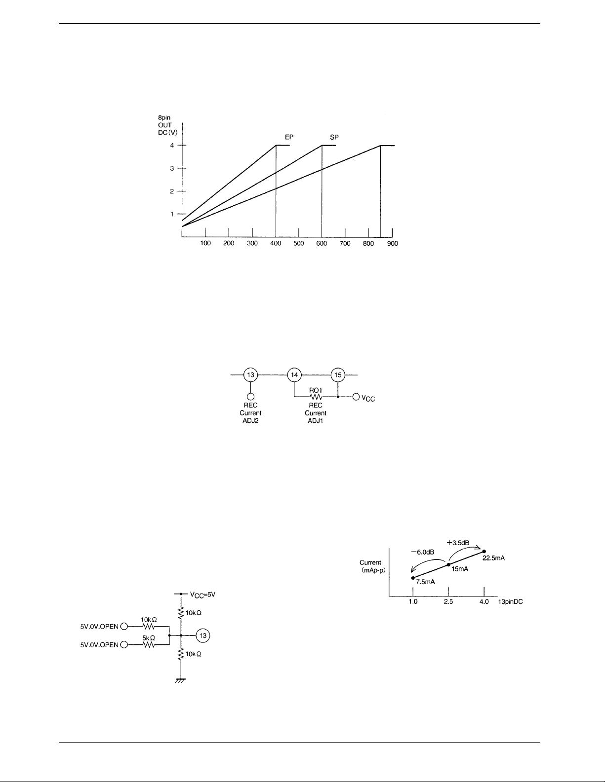
2. Envelope Detector Characteristics: pin 8
The LA6529M includes an on-chip playback signal envelope detector circuit used to achieve automatic tracking
adjustment with essentially linear characteristics.
Envelope Detector Characteristics (design target values) f = 4 MHz
Pin 8 + external 18 kΩ resistor
SP + external 18 kΩ resistor
Pin 10 playback amplifier output level (mVp-p)
3. Record Amplifier Gain Control
The LA6529M achieves an adjustment-free record current by adding an AGC circuit in the record amplifier block. The
record current can be modified using the circuit shown below.
(1) REC Current.Adj2: When open
The pin 13 DC level is set to 1/2 VCC(about 2.5 V) by an internal bias and the record current is determined by RO1.
Design values: RO1: 1.5 kΩ = 15.6 mAp-p (SP) (per channel)
= 12.3 mAp-p (EP)
(2) REC Current.Adj2: When used
The value determined by RO1 can be adjusted from –6.0 dB to +3.5 dB by applying a control DC level (1 to 4 V) to pin 13.
(Reference)
The circuit below can be used to apply the DC control level to pin 13.
This allows 9 modes (1 to 4 V) to be applied.
Microcontroller
Design values
No. 5647-6/12
Page 7
LA7415
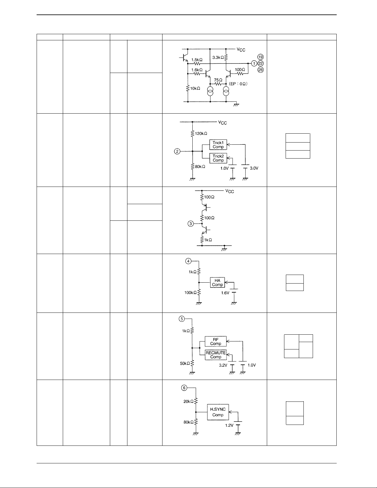
Pin Functions
Pin No. Pin Standard DC voltage (V) Pin circuit Notes
PB 2.0
1
19 PB Amp
22 Second filter
28
REC 3.6
3.0 V
2 TRICK-H
High: 4.5 V or higher
PB
Low: 0.7 V or lower
3 COMP-OUT EP > SP ENV: High
REC OPEN
4 HA (EP/SP)
1.0 V
1.6 V
Trick1
NORMAL
Trick2
EP
SP
5 RF-SW
(REC-MUTE) 1.0 (V) Lch
6 H-SYNC
SW30 REC MUTE
Hch
Sync
1.5 V
H
L
Continued on the next page.
ON 3.2 (V)
OFF
No. 5647-7/12
Page 8
LA7415
Continued from the preceding page.
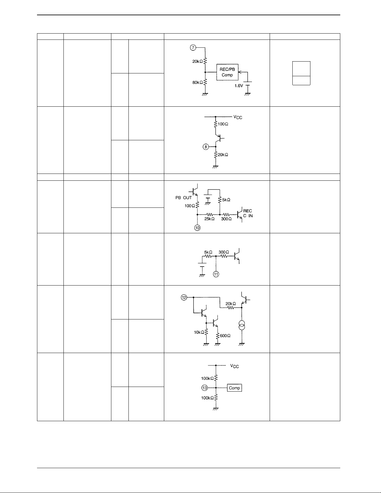
Pin No. Pin Standard DC voltage (V) Pin circuit Notes
PB 0
7 REC-H
8 ENV DET OUT
9 GND
PB-OUT PB 2.3
10
REC-C-IN REC 3.6
REC 5
Described
PB in a separate
document.
REC 0
2.0 V
REC
PB
11 REC-Y-IN REC 3.6
PB 1.6
12 AGC-FLT
REC 1.6
PB 2.5
13 REC-CURRENT ADJ2
REC 2.5
4 V: +3.5 dB
2.5 V: ±0 dB
(OPEN)
1 V: –6 dB
Continued on the next page.
No. 5647-8/12
Page 9
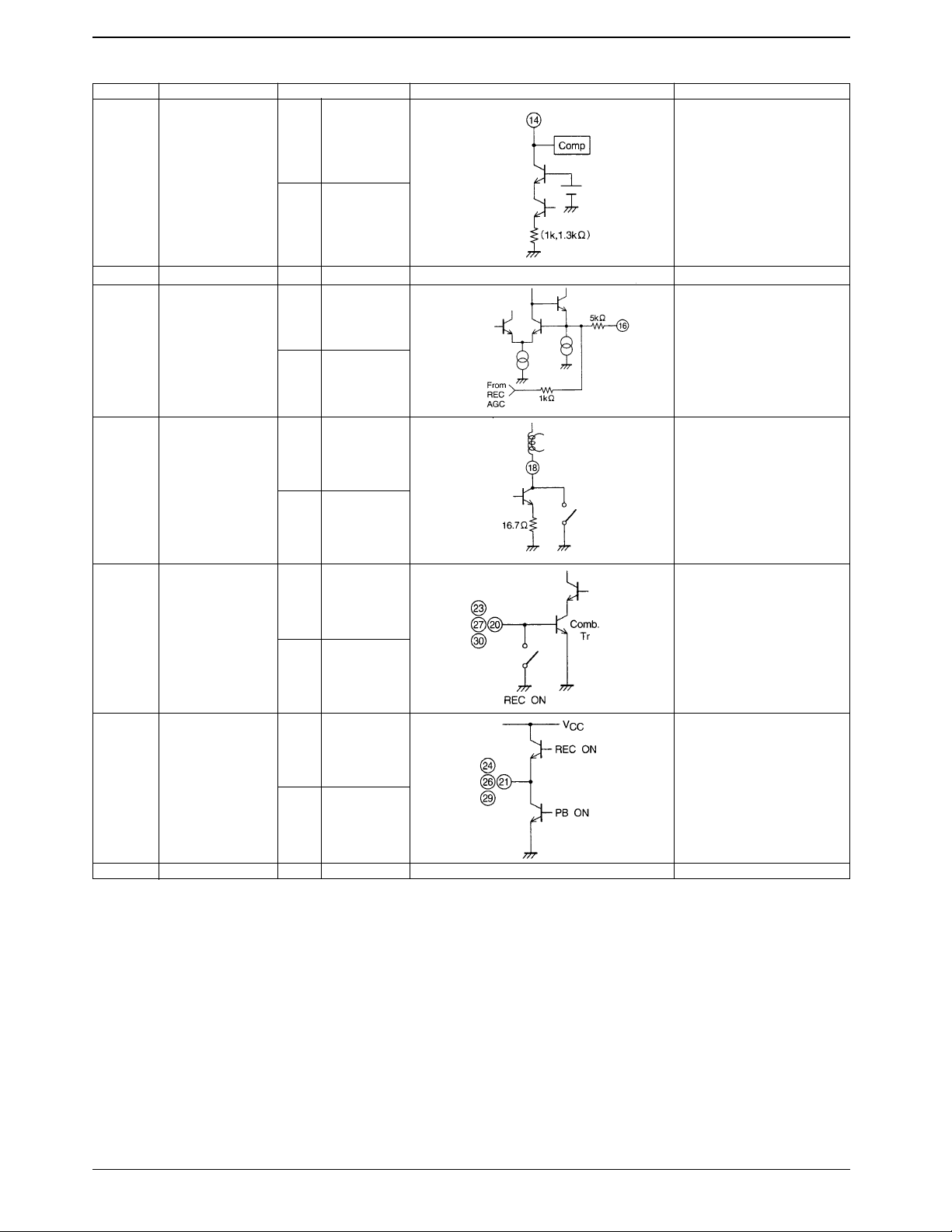
LA7415
Continued from the preceding page.
Pin No. Pin Standard DC voltage (V) Pin circuit Notes
PB 4.5
14 REC-CURRENT ADJ1
REC 5.0
15 V
16 REC-BIAS
17 REC-SP OUT
18 REC-EP OUT
20 SP-L-IN
23 SP-H-IN
27 EP-L-IN
30 EP-H-IN
CC
PB 2.5
REC 1.7
PB 0
REC 4.2
PB 0.7
REC 0
21 SP-L-SW
24 SP-H-SW
26 EP-L-SW
29 EP-H-SW
25 PRE-GND
PB 0
REC 4.2
No. 5647-9/12
Page 10
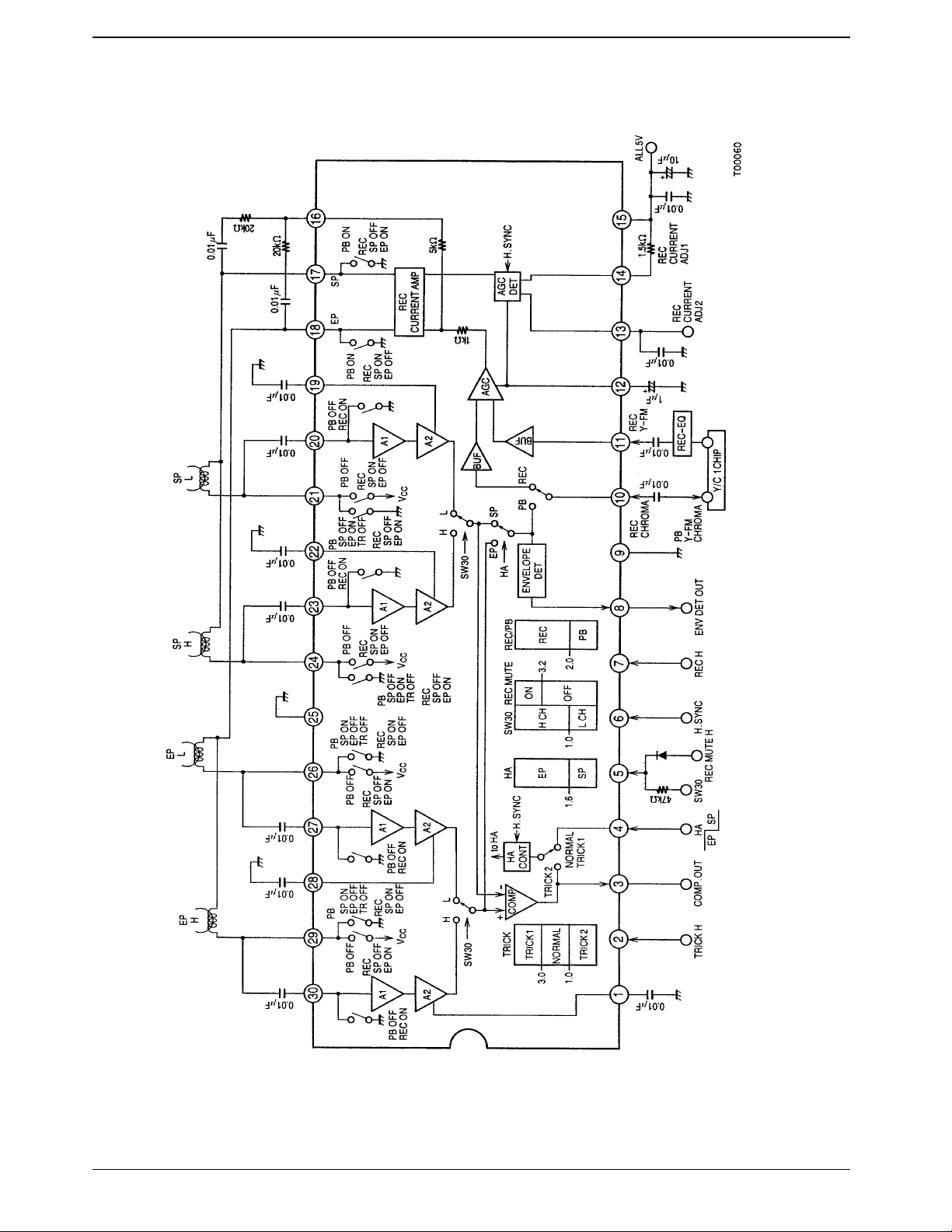
Block Diagram
LA7415
No. 5647-10/12
Page 11
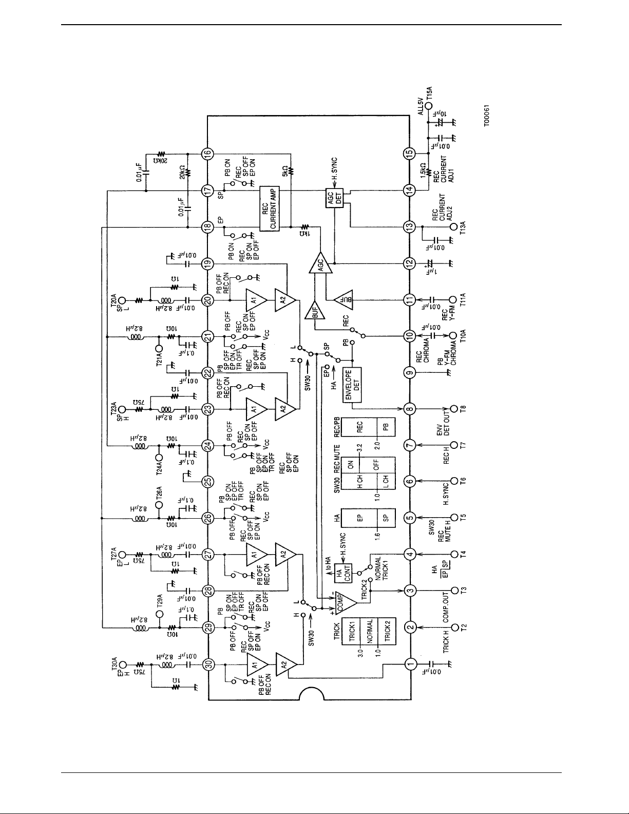
Test Circuit
LA7415
No. 5647-11/12
Page 12

LA7415
■ No products described or contained herein are intended for use in surgical implants, life-support systems, aerospace
equipment, nuclear power control systems, vehicles, disaster/crime-prevention equipment and the like, the failure of
which may directly or indirectly cause injury, death or property loss.
■ Anyone purchasing any products described or contained herein for an above-mentioned use shall:
➀ Accept full responsibility and indemnify and defend SANYO ELECTRIC CO., LTD., its affiliates, subsidiaries and
distributors and all their officers and employees, jointly and severally, against any and all claims and litigation and all
damages, cost and expenses associated with such use:
➁ Not impose any responsibility for any fault or negligence which may be cited in any such claim or litigation on
SANYO ELECTRIC CO., LTD., its affiliates, subsidiaries and distributors or any of their officers and employees
jointly or severally.
■ Information (including circuit diagrams and circuit parameters) herein is for example only; it is not guaranteed for
volume production. SANYO believes information herein is accurate and reliable, but no guarantees are made or implied
regarding its use or any infringements of intellectual property rights or other rights of third parties.
This catalog provides information as of April, 1997. Specifications and information herein are subject to change
without notice.
No. 5647-12/12
 Loading...