

Page 1
Overview
The LA7357 can be used as a PAL/SECAM
discrimination IC. Since no ceramic resonator or tank
circuit is required, only a small number of external
components are used, and the LA7357 can contribute to
reduced mounting areas and lower system costs.
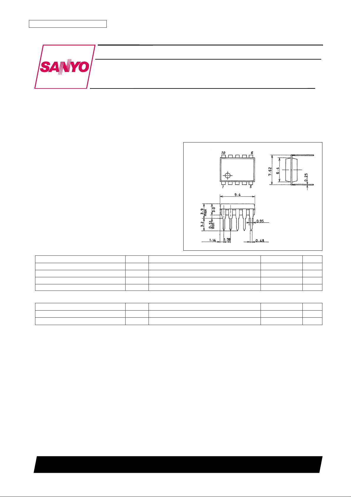
Package Dimension
unit: mm
3098B-DIP10S
Monolithic Linear IC
Ordering number : EN5654
73097HA(OT) No. 5654-1/6
SANYO: DIP10S
[LA7357]
SANYO Electric Co.,Ltd. Semiconductor Bussiness Headquarters
TOKYO OFFICE Tokyo Bldg., 1-10, 1 Chome, Ueno, Taito-ku, TOKYO, 110 JAPAN
PAL/SECAM Discrimination Circuit for VHS VCRs
LA7357
Parameter Symbol Conditions Ratings Unit
Maximum supply voltage V
CC
max 7.0 V
Allowable power dissipation Pd max Ta ≤ 65 °C 120 mW
Operating temperature Topr –10 to +65 °C
Storage temperature Tstg –40 to +125 °C
Parameter Symbol Conditions Ratings Unit
Supply voltage V
CC
5.0 V
Operating voltage range V
CC
op 4.8 to 5.5 V
Operating Conditions at Ta = 25°C
Specifications
Maximum Ratings at Ta = 25°C
Page 2
No. 5654-2/6
LA7357
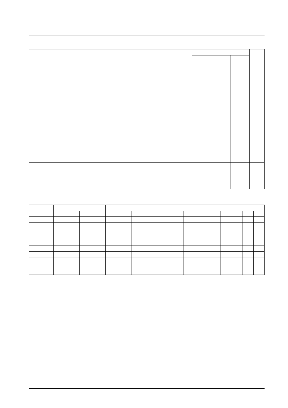
Parameter Symbol Conditions
Ratings
Unit
min typ max
Current drain
I
CC
1 Pin 5 = ground, pin 7 influx current: T4 output 7.0 10.0 13.0 mA
I
CC
2 Pin 5 = VCC, pin 7 influx current: T4 output 7.5 10.5 13.5 mA
The pin 5 voltage when the pin 2 output
appears when slowly raising the voltage
BGP threshold level BTH applied to pin 5 from 0 V. 2.2 2.5 2.8 V
The input signal should be 300 mVp-p:
T2 output
The pin 5 voltage when the pin 2 output
appears when slowly lowering the voltage
SYNC threshold level STH applied to pin 5 from 5 V. 0.6 0.8 1.0 V
The input signal should be 300 mVp-p:
T2 output
Stipulated as the output ratio when a
Input limiter amplifier gain LIMG 10 mVp-p amplitude sine wave is input to 9 12 15 dB
pin 1: T2 output
Measure the output amplitude when a
Input limiter amplifier level LIMD 300 mVp-p amplitude sine wave is input to 150 190 230 mVp-p
pin 1: T2 output
The V1 level when T1 switches from low to
Comparator hysteresis high-level voltage Comp H high when slowly raising V1 from 0 V: T1 2.7 3.0 3.3 V
output
The V1 level when T1 switches from high to
Comparator hysteresis low-level voltage Comp L low when slowly lowering V1 from 5 V: T1 2.0 2.3 2.6 V
output
DET-OUT output high-level voltage DETH With a 2-kΩ load: T1 output 3.6 4.0 4.4 V
DET-OUT output low-level voltage DETL With a 2-kΩ load: T1 output 0 0.2 0.4 V
Operating Characteristics at Ta = 25°C, VCC= 5 V
Switching Conditions
Symbol
Input signal Input pulse Applied voltage Switch states
S1 S2 S3 S4 V1 V2 SW1 SW2 SW3 SW4 SW5
I
CC
1 No signal No signal 0 V 0 V Off Off Off Off Off
I
CC
2 No signal No signal 5 V 5 V Off Off Off Off Off
BTH Sig.1 No signal1 0 V 0 V
Variable DC level
On Off On Off Off
STH No signal Sig.1 0 V 0 V
Variable DC level
On Off On Off Off
LIMG Sig.1 No signal 5 V 0 V On Off Off Off Off
LIMD Sig.1 No signal 5 V 0 V On Off Off Off On
Comp H No signal No signal No signal No signal
Variable DC level
Off On Off Off On
Comp L No signal No signal No signal No signal
Variable DC level
Off On Off Off On
DETH Sig.2 Sig.1 P2 P1 Off Off Off Off On
DETL Sig.3 Sig.1 P2 P1 Off Off Off Off On
Page 3
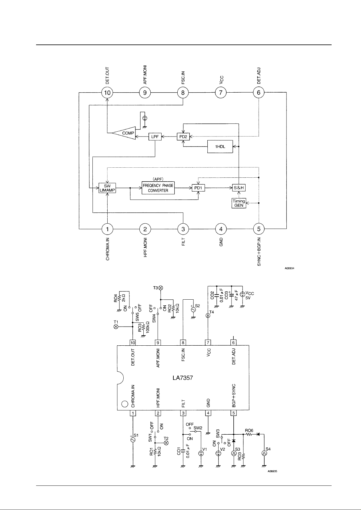
Block Diagram
Test Circuit
No. 5654-3/6
LA7357
Page 4
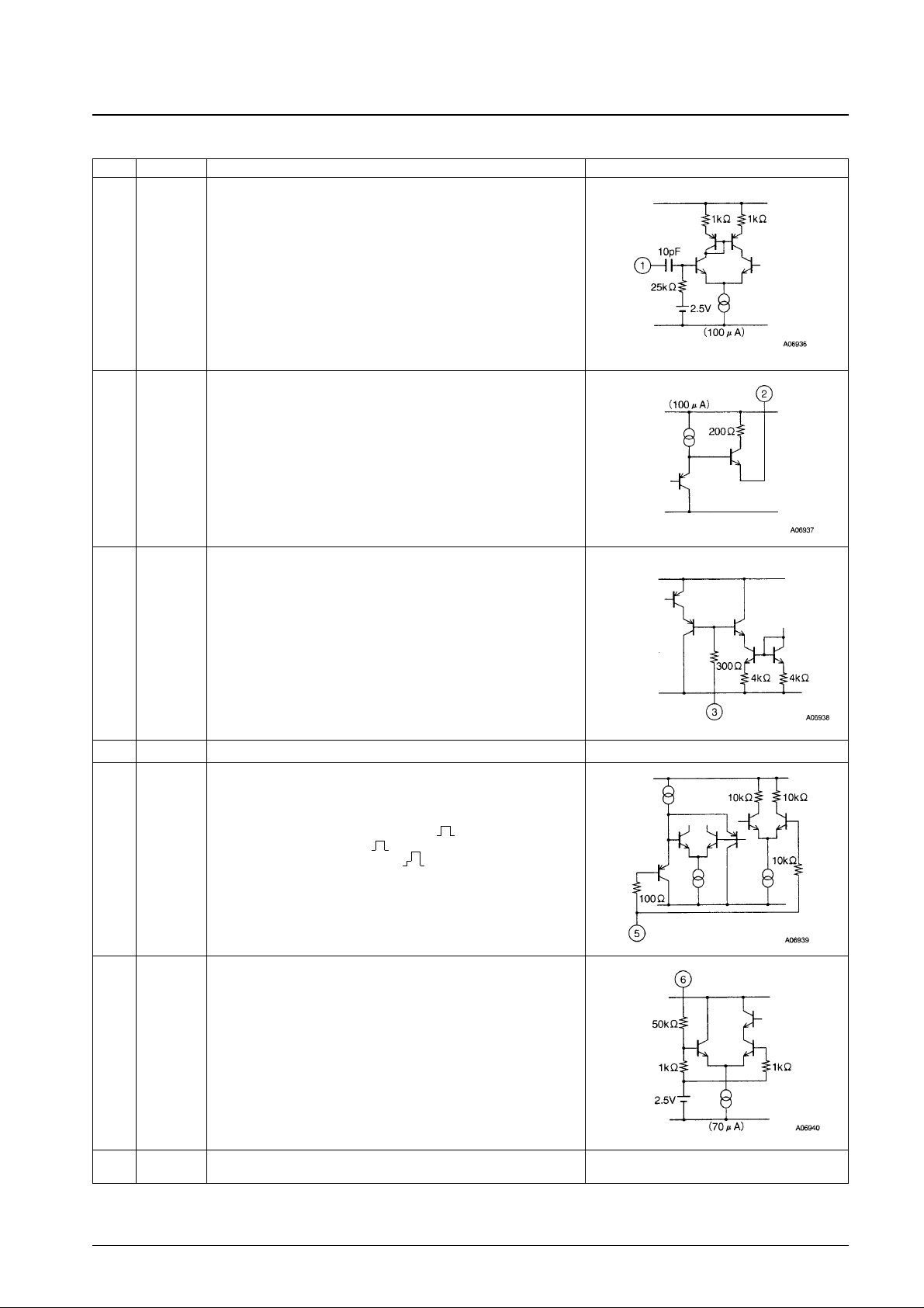
Pin No. Pin Pin Functions Equivalent circuit
No. 5654-4/6
LA7357
Pin Functions
1 CHROMA-IN
• Chrominance signal input. This pin can handle burst (or unmodulated
carrier for SECAM input) signal amplitudes of between 50 and 800 mVp-p.
2 HPF.MONI
• High-pass filter output monitor
To avoid interference between pin 1 and pin 3, this pin should be
connected to V
CC
during normal operation.
3 FILTER
• Phase comparator output
This signal is smoothed with an external capacitor.
The smoothed level will be:
2.0 V or lower for PAL
3.5 V or higher for SECAM or MESECAM.
4 GND
5 SYNC+BGP
• BGP + SYNC input
The input level is a 1.0- to 2.0-V rising pulse ( ) during the SYNC period,
and a 3.0- to 4.5-V rising pulse ( ) during the BGP period. Note that since
a combined BGP and C.SYNC pulse ( ) is output from the Y/C IC when
the LA7357 is used in combination with a Sanyo single-chip Y/C IC (any
one of the LA7430, LA7435, or LA71520) no external component will be
required on pin 5.
6 DET-ADJ
7
V
CC
• Discrimination sensitivity adjustment pin
The discrimination is shifted towards PAL as the pin voltage is increased,
and towards SECAM as the pin voltage is lowered.
This pin is normally left open.
Continued on next page.
Page 5
No. 5654-5/6
LA7357
Continued from preceding page.
Pin No. Pin Pin Functions Equivalent circuit
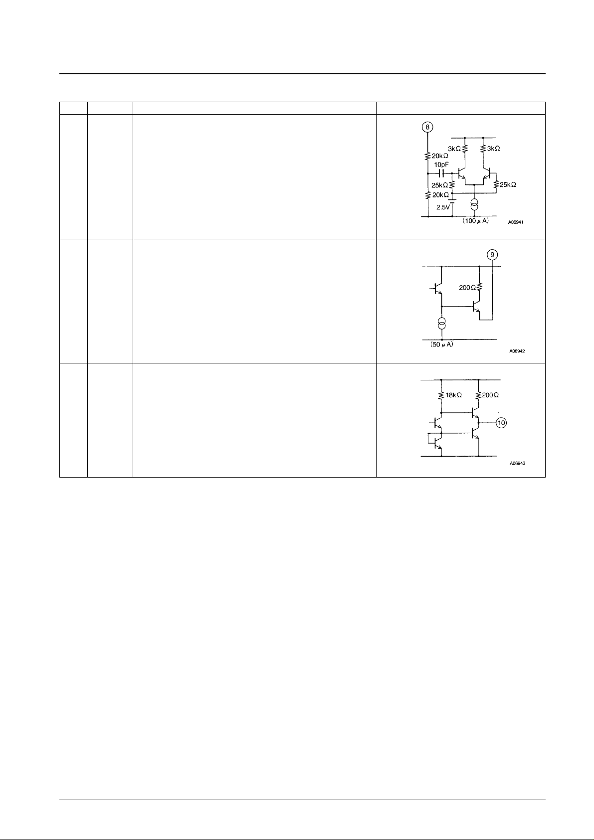
8 FSC-IN
• PAL fsc (4.43 MHZ) input
This pin can handle inputs with amplitude between about 300 and 800
mVp-p.
9 AFP.MONI
• APF output monitor
This pin must be connected to V
CC
to prevent interference between pins 8
and 10.
10 DET-OUT
• Discrimination output
This pin outputs a high level (4.2 V) for SECAM or MESECAM inputs, and a
low level (close to 0 V) for PAL inputs.
Page 6
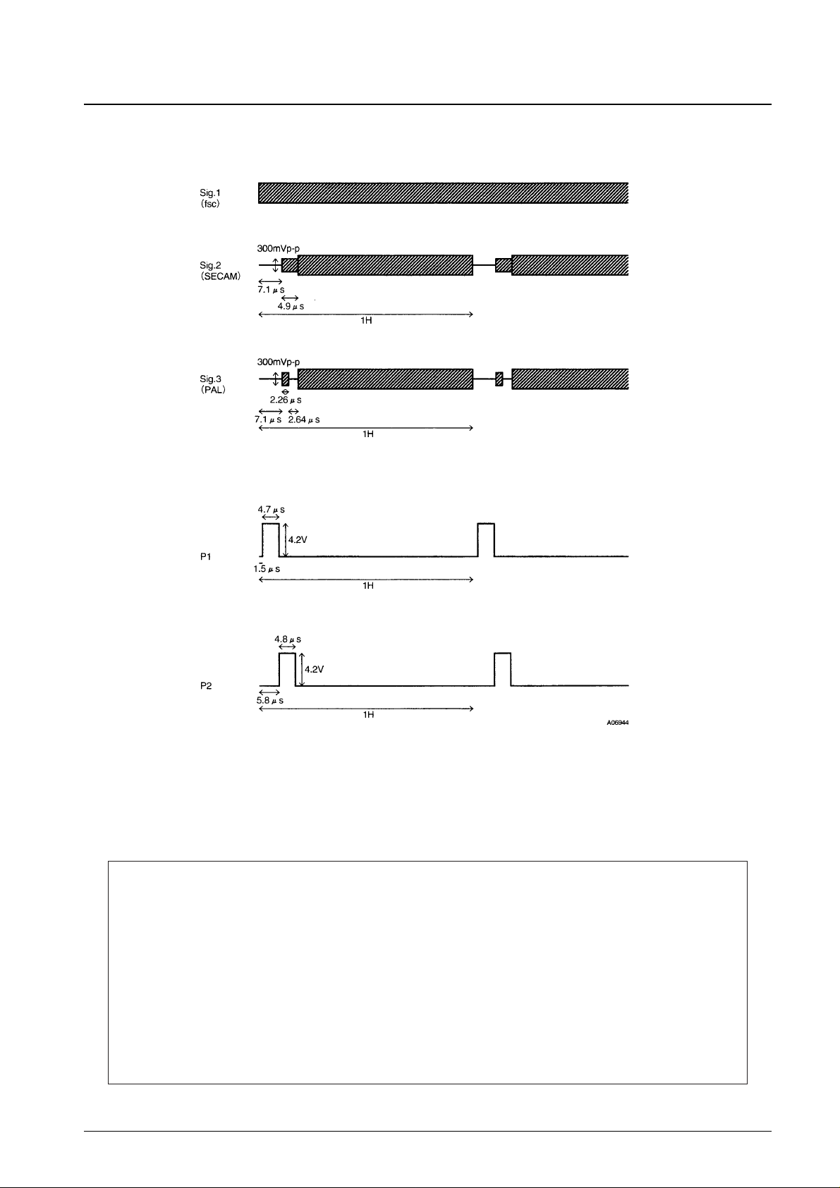
Test Input Signals and Pulses
No. 5654-6/6
LA7357
fsc sine wave
SECAM color bar signal
PAL color bar signal
This catalog provides information as of July, 1997. Specifications and information herein are subject to change
without notice.
■ No products described or contained herein are intended for use in surgical implants, life-support systems, aerospace
equipment, nuclear power control systems, vehicles, disaster/crime-prevention equipment and the like, the failure of
which may directly or indirectly cause injury, death or property loss.
■ Anyone purchasing any products described or contained herein for an above-mentioned use shall:
➀ Accept full responsibility and indemnify and defend SANYO ELECTRIC CO., LTD., its affiliates, subsidiaries and
distributors and all their officers and employees, jointly and severally, against any and all claims and litigation and all
damages, cost and expenses associated with such use:
➁ Not impose any responsibility for any fault or negligence which may be cited in any such claim or litigation on
SANYO ELECTRIC CO., LTD., its affiliates, subsidiaries and distributors or any of their officers and employees
jointly or severally.
■ Information (including circuit diagrams and circuit parameters) herein is for example only; it is not guaranteed for
volume production. SANYO believes information herein is accurate and reliable, but no guarantees are made or implied
regarding its use or any infringements of intellectual property rights or other rights of third parties.
 Loading...