

Page 1
Monolithic Linear IC
Ordering number : N5288A
13097 HA (OT) No. 5288-1/7
SANYO Electric Co.,Ltd. Semiconductor Bussiness Headquarters
TOKYO OFFICE Tokyo Bldg., 1-10, 1 Chome, Ueno, Taito-ku, TOKYO, 110 JAPAN
SECAM-Format VCR
Chroma Signal-Processing Circuit
LA7337
Overview
The LA7337 is an IC that implements SECAM-format
VCR signal processing in a single chip. It incorporates
band-pass filters and a SECAM discrimination circuit on
chip and features automatic adjustment of the bell filter for
a reduced number of external components and adjustmentfree circuit operation.
Features
• All required filters, except for the bell filter,
incorporated on chip.
• Automatic adjustment of the bell filter f0parameter
• Built-in SECAM discrimination circuit
Functions
•4.3-MHz and 1.1-MHz band-pass filters, limiter, AGC (in
playback mode)
• Divide-by-four circuit, 4× frequency multiplier circuit,
2.2-MHz band-pass filter
• Bell filter f0automatic adjustment circuit, SECAM
discrimination circuit
• Sync gate
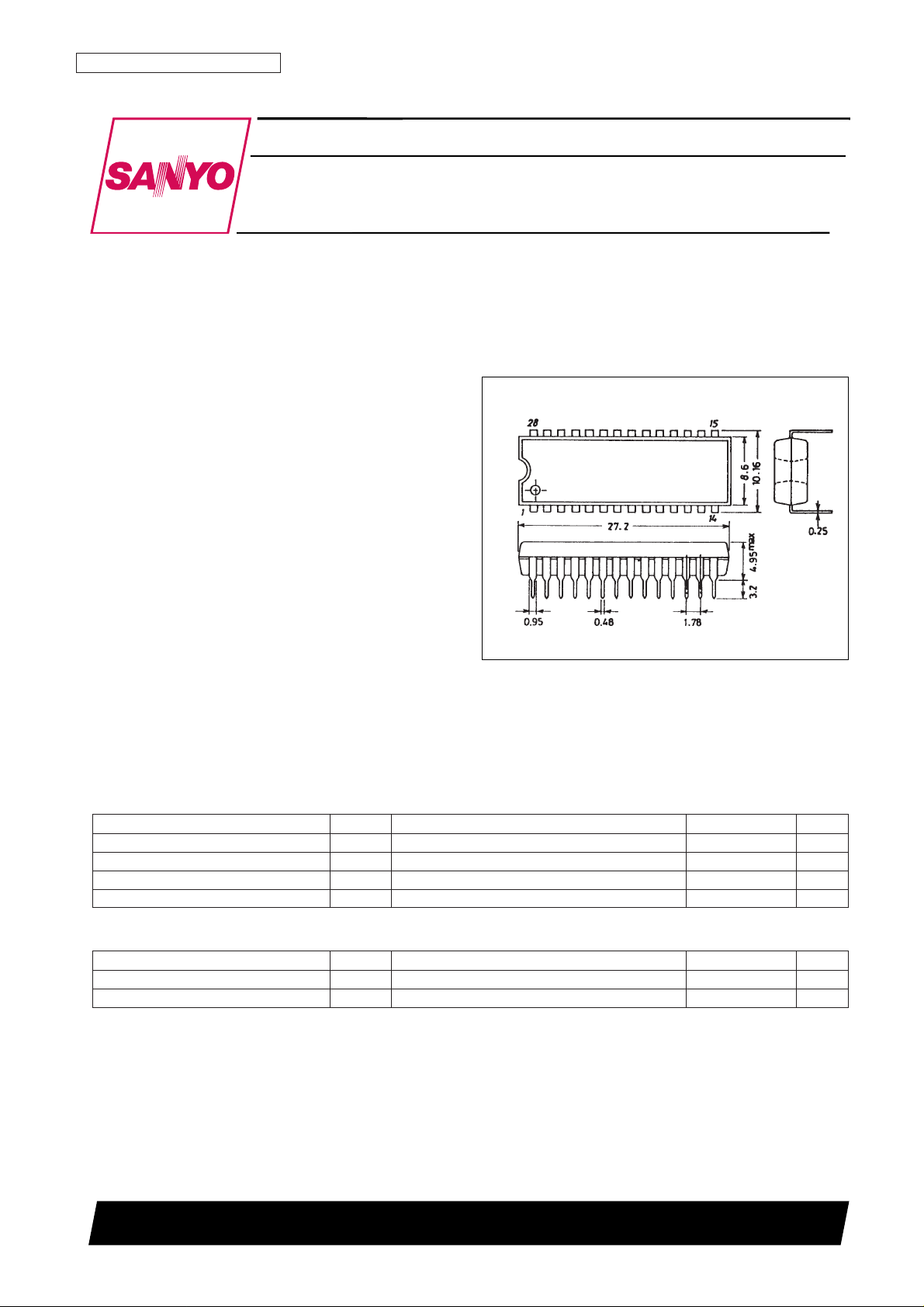
Package Dimensions
unit: mm
3063-DIP28S
SANYO: DIP28S
[LA7337]
Parameter Symbol Conditions Ratings Unit
Maximum supply voltage V
CC
max 7V
Allowable power dissipation Pd max Ta ≤ 70°C 600 mW
Operating temperature Topr –15 to +70 °C
Storage temperature Tstg –40 to +150 °C
Specifications
Absolute Maximum Ratings at Ta = 25°C
Parameter Symbol Conditions Ratings Unit
Recommended supply voltage V
CC
5V
Operating supply voltage range V
CC
op 4.8 to 5.5 V
Operating Conditions at Ta = 25°C
Page 2
No. 5288-2/7
LA7337
Parameter Symbol Conditions
Ratings
Unit
min typ max
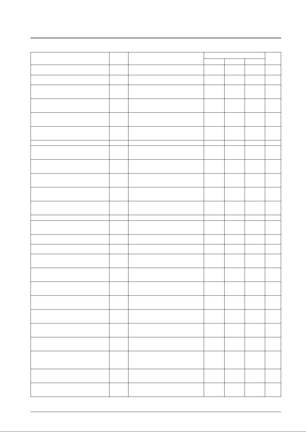
Record mode current drain I
CCR
V5 = V6 = 0 V, V16 = 0 V, S27 = composite
50 70 90 mA
sync., S15 = color bar signal
4.3-MHz band-pass filter characteristics (1) V
F4C
V6 = 5 V, V16 = 0 V, S27 = composite sync.
145 180 215 mVp-p
S15 = sine wave (200 mVp-p, f = 4.286 MHz)
As above, except S15 = sine wave
4.3-MHz band-pass filter characteristics (2) G
F4L1
(200 mVp-p, f = 1.1 MHz), taking V
F4C
as the –30 –20 dB
reference (0 dB)
As above, except S15 = sine wave
4.3-MHz band-pass filter characteristics (3) G
F4L2
(200 mVp-p, f = 2.2 MHz), taking V
F4C
as the –10 –5 dB
reference (0 dB)
As above, except S15 = sine wave
4.3-MHz band-pass filter characteristics (4) G
F4H
(200 mVp-p, f = 7.5 MHz), taking V
F4C
as the –30 –20 dB
reference (0 dB)
V5 = V6 = 0 V, V16 = 0 V, SW21B = on,
Record mode bell filter center frequency (1) F
BLR1
S15 = sine wave (200 mVp-p, f = 4 to 5 MHz), 4.243 4.286 4.329 MHz
S27 = composite sync.
Record mode bell filter center frequency (2) F
BLR2
As above, except V5 = 4 V. 4.493 4.536 4.579 MHz
V5 = V6 = 0 V, V16 = 0 V, SW21B = on,
Record mode bell filter characteristics (1) V
BLRC
S15 = sine wave (200 mVp-p, f = FBLR1), 200 250 300 mVp-p
S27 = composite sync.
As above, except S15 = sine wave
Record mode bell filter characteristics (2) G
BLRL
(200 mVp-p, f = 3.8 MHz), taking V
BLRC
as –14 –11 –8 dB
the reference (0 dB)
As above, except S15 = sine wave
Record mode bell filter characteristics (3) G
BLRH
(200 mVp-p, f = 4.8 MHz), taking V
BLRC
as –14 –11 –8 dB
the reference (0 dB)
V5 = V6 = 0 V, S15 = a SECAM color bar
Record mode killer operating level G
KLR
signal (variable level), V16 = 0 V, SW21B = on,
–28 –23 –18 dB
V23 = 3.4 V, V24 = 3.7 V, S27 = composite sync.
SW1 = on, V1 = 5 V, V5 = V6 = 0 V, V16 = 0 V,
Record equalization center frequency (1) F
EQR1
S21 = sine wave (200 mVp-p, f = 4 to 5 MHz),
1.0608 1.0715 1.0822 MHz
SW21A = SW21B = on, S27 = composite sync.
Record equalization center frequency (2) F
EQR2
As above, except V6 = 4 V 1.0788 1.0895 1.1002 MHz
SW1 = on, V1 = 5 V, V5 = V6 = 0 V, V16 = 0 V,
Record equalization characteristics (1) V
EQRC
S21 = sine wave (200 mVp-p, f = FEQR1 × 4),
65 85 105 mVp-p
SW21A = SW21B = on, S27 = composite sync.
Record equalization characteristics (2) G
EQRL
As above, except S21 = sine wave (200 mVp-p,
8 11 14 dB
f = 3.8 MHz), taking V
EQRC
as the reference (0 dB)
Record equalization characteristics (3) G
EQRH
As above, except S21 = sine wave (200 mVp-p,
8 11 14 dB
f = 4.8 MHz), taking V
EQRC
as the reference (0 dB)
SW1 = on, V1 = 5 V, V5 = V6 = 0 V, V16 = 0 V,
Record chrominance signal output level V
OR
S15 = sine wave (200 mVp-p, f = 4.4 MHz), 80 110 140 mVp-p
SW21B = on, S27 = composite sync.
Record chrominance signal output unnecessary
As above, except measure the 2.2 MHz
spectrum (1)
GSR1 component in the T11 signal. Taking V
OR
as –30 –20 dB
the reference (0 dB).
Record chrominance signal output unnecessary
As above, except measure the 3.3 MHz
spectrum (2)
GSR2 component in the T11 signal. Taking V
OR
as –30 –20 dB
the reference (0 dB).
V5 = V6 = 0 V, V16 = 5 V, S27 = composite
Playback mode current drain I
CCP
sync., S13 = sine wave 60 80 100 mA
(50 mVp-p, f = 1.0715 MHz)
V6 = 5 V, SW8B = on, V16 = 5 V,
AGC control characteristics (1) V
AGC
S27 = composite sync., S13 = sine wave 90 120 150 mVp-p
(50 mVp-p, f = 1.0715 MHz)
As above, except S13 = sine wave
AGC control characteristics (2) G
AGC1
(100 mVp-p, f = 1.0715 MHz) –1 0 +1 dB
Taking V
AGC
as the reference (0 dB).
As above, except S13 = sine wave
AGC control characteristics (3) G
AGC2
(25 mVp-p, f = 1.0715 MHz) –1 0 +1 dB
Taking V
AGC
as the reference (0 dB).
V6 = 5 V, SW14 = on, V14 = V14R,
1.1-MHz band-pass filter characteristics (1) G
F1L
S13 = sine wave (50 mVp-p, f = 500 kHz),
–3 0 +3 dB
V16 = 5 V, S27 = composite sync., taking
VAGC as the reference (0 dB).
As above, except S13 = sine wave
1.1-MHz band-pass filter characteristics (2) G
F1H1
(50 mVp-p, f = 2.2 MHz) –30 –20 dB
Taking V
AGC
as the reference (0 dB).
As above, except S13 = sine wave
1.1-MHz band-pass filter characteristics (3) G
F1H2
(50 mVp-p, f = 3.3 MHz) –35 –25 dB
Taking V
AGC
as the reference (0 dB).
Operating Characteristics at Ta = 25°C, VCC= 5 V
Continued on next page.
Page 3
No. 5288-3/7
LA7337
Continued from preceding page.
Parameter Symbol Conditions
Ratings
Unit
min typ max
V6 = 0 V, SW8B = on, SW14 = on,
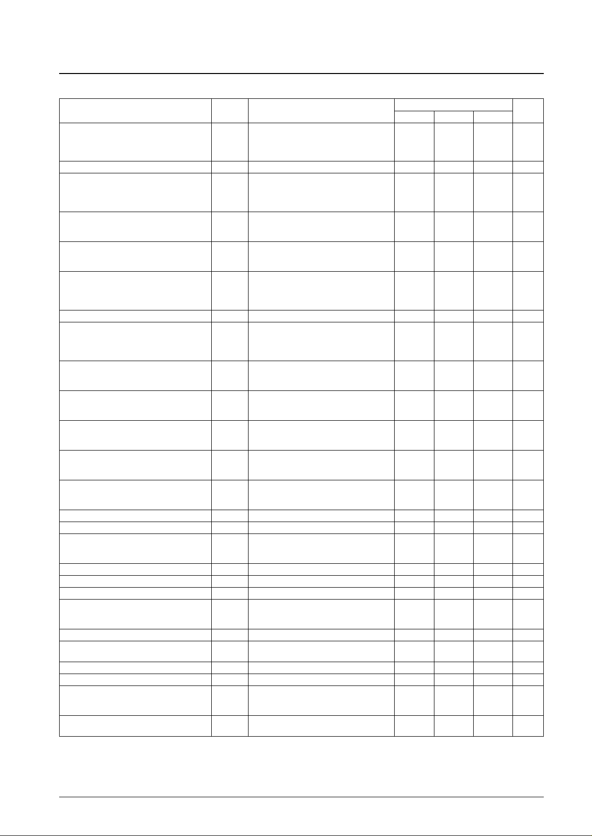
Playback equalization center frequency (1) F
EQP1
V14 = V14R, S13 = sine wave
1.0608 1.0715 1.0822 MHz
(50 mVp-p, f = 1 to 1.2 MHz), V16 = 5 V,
S27 = composite sync.
Playback equalization center frequency (2) F
EQP2
As above, except V6 = 4 V 1.0788 1.0895 1.1002 MHz
V6 = 0 V, SW8B = on, SW14 = on,
Playback equalization characteristics (1) V
EQPC
V14 = V14R, S13 = sine wave
120 150 180 mVp-p
(50 mVp-p, f = FEQP1), V16 = 5 V,
S27 = composite sync.
As above, except S13 = sine wave
Playback equalization characteristics (2) G
EQPL
(50 mVp-p, f = 950 kHz), taking V
EQP
as the –14 –11 –8 dB
reference (0 dB).
As above, except S13 = sine wave
Playback equalization characteristics (3) G
EQPH
(50 mVp-p, f = 1.2 MHz), taking V
EQP
as the –14 –11 –8 dB
reference (0 dB).
SW1 = on, V1 = 5 V, V5 = V6 = 0 V,
Playback bell center frequency (1) F
BLP1
SW8A = SW8B = on, V16 = 5 V,
4.243 4.286 4.329 MHz
S27 = composite sync., S8 = sine wave
(200 mVp-p, f = 1 to 1.2 MHz),
Playback bell center frequency (2) F
BLP2
As above, except V5 = 4 V 4.493 4.536 4.579 MHz
SW1 = on, V1 = 5 V, V5 = V6 = 0 V,
Playback bell characteristics (1) V
BLPC
SW8A = SW8B = on, S8 = sine wave
65 85 105 mVp-p
(200 mVp-p, f = FBLP × 1/4), V16 = 5 V,
S27 = composite sync.
As above, except S8 = sine wave
Playback bell characteristics (2) G
BLPL
(200 mVp-p, f = 950 kHz), taking V
BLPC
as 8 11 14 dB
the reference (0 dB).
As above, except S8 = sine wave
Playback bell characteristics (3) G
BLPH
(200 mVp-p, f = 1.2 MHz), taking V
BLPC
as 8 11 14 dB
the reference (0 dB).
SW1 = on, V1 = 5 V, V5 = V6 = 0 V, V16 = 5 V,
Playback chrominance signal output level V
OP
S13 = sine wave (200 mVp-p, f = 1.1 MHz), 130 160 190 mVp-p
SW8B = on, S27 = composite sync.
Playback chrominance signal output
As above, except measure the 2.2 MHz
unnecessary spectrum (1)
GSP1 component in the T17 signal. Taking V
OP
as –25 –15 dB
the reference (0 dB).
Playback chrominance signal output
As above, except measure the 3.3 MHz
unnecessary spectrum (2)
GSP2 component in the T17 signal. Taking V
OP
as –20 –10 dB
the reference (0 dB).
CLK input level V
CLK
f = 4.433619 MHz 100 200 800 mVp-p
Synchronizing signal input threshold level V
THS
1.8 2 2.2 V
SW1 = on, V1 = 5 V, V5 = V6 = 0 V, V16 = 0 V,
Record mode sync gate start time (muting off) T
RGB
S15 = sine wave (200 mVp-p, f = 4.286 MHz), –0.3 +0.2 +0.7 µs
SW21B = on, S27 = composite sync.
Record mode sync gate start time (muting on) T
RGBM
As above, except SW2 = on 1.5 2 2.5 µs
Record mode sync gate release time T
RGE
As above 4.5 5.0 5.5 µs
Record mode mute setting resistance VTSP2 10 20 30 kΩ
SW1 = on, V5 = V6 = 0 V, SW8B = on,
Playback mode sync gate start time T
PGB
S13 = sine wave (50 mVp-p, f = 1.0715 MHz), 1.5 2 2.5 µs
V16 = 5 V, S27 = composite sync.
Playback mode sync gate release time T
PGE
As above 4.5 5.0 5.5 µs
BGP start time T
BGB
V5 = 0 V, V6 = 5 V, SW21B = on, V16 = 0 V,
6.0 6.5 7.0 µs
S27 = composite sync.
BGP amplitude T
BGW
As above 2.0 2.5 3.0 µs
SECAM discriminator output resistance R26 SW25 = on, V25 = 5 V 7 10 13 kΩ
Record mode SECAM discriminator
V5 = V6 = 0 V, V16 = 0 V, SW21B = on,
characteristics (1)
V
SCMR1
S27 = composite sync., S15 = SECAM color 4.5 V
bar signal
Record mode SECAM discriminator
V
SCMR2
As above, except S15 = PAL color bar signal 0.5 V
characteristics (2)
Continued on next page.
Page 4

No. 5288-4/7
LA7337
[Record/playback mode settings]
Pin 16 = low → record mode
Pin 16 = high → playback mode
[Bell filter offset adjustment]
Increasing the pin 6 voltage increases the 1.1-MHz bell filter center frequency (f0).
Increasing the pin 5 voltage increases the 4.3-MHz bell filter center frequency (f0).
[Test mode settings]
The IC enters test mode if pin 6 is set to 5 V. The pin 5, 11, 17, and 26 outputs behave as follows in this mode.
Pin 5: The 4.43-MHz VCO output appears (However, note that a load of about 1 kΩ is required between this pin and
VCC.)
Pin 11: The 1.1-MHz band-pass filter output appears.
Pin 17: The 4.3-MHz band-pass filter output appears.
Pin 26: The BGP (used for SECAM discrimination, playback AGC, and record killer) can be monitored.
Standard Input Signal Levels
Continued from preceding page.
Parameter Symbol Conditions
Ratings
Unit
min typ max
Playback mode phase detector output
V5 = V6 = 0 V, SW8B = on, V16 = 5 V,
difference voltage (1)
V
SCPD1
S27 = composite sync., S13 = sine wave 150 180 mV
(50 mVp-p, f = 1.0625/1.1016 MHz)
Playback mode phase detector output
V
SCPD2
As above, except S13 = sine wave
100 mV
difference voltage (2) (50 mVp-p, f = 627 kHz)
Playback mode SECAM discriminator
V
SCMP1
V16 = 5 V, SW23 = SW24 = On 4.5 V
characteristics (1)
Playback mode SECAM discriminator
V
SCMP2
V16 = 5 V, SW23 = SW24 = On 0.5 V
characteristics (2)
SECAM discriminator comparator
V
TCOMP
SW25 = On 3.2 3.5 3.8 V
threshold voltage
Record/playback control threshold voltage V
TRP
2.3 2.5 2.7 V
V16 = 0 V, SW25 = on, V25 = 3 V,
Forced SECAM mode threshold voltage V
THSM
S27 = composite sync., S15 = sine wave 4 V
(200 mVp-p, f = 4.286 MHz)
V16 = 0 V, SW25 = on, V25 = 4 V,
Forced mute mode threshold voltage V
THMM
S27 = composite sync., S15 = sine wave 1 V
(200 mVp-p, f = 4.286 MHz)
Reference voltage V
REG
4.1 4.3 4.5 V
REC-IN (pin 15) The 200 mVp-p ID component
PB-IN (pin 13) 50 mVp-p
Internal filter group delay times (reference values)
1.1 MHz BPF 460 ns (PB) 430 ns (REC)
2.2 MHz BPF 180 ns
4.3 MHz BPFA 230 ns
4.3 MHz BPFB 170 ns
[Muting control table]
Voltage applied to pin 1 Output signal mode (pins 17 and 11)
4 V or higher Forced SECAM
Open AUTO (Uses the output of the internal discriminator)
1 V or lower Forced mute mode
Page 5
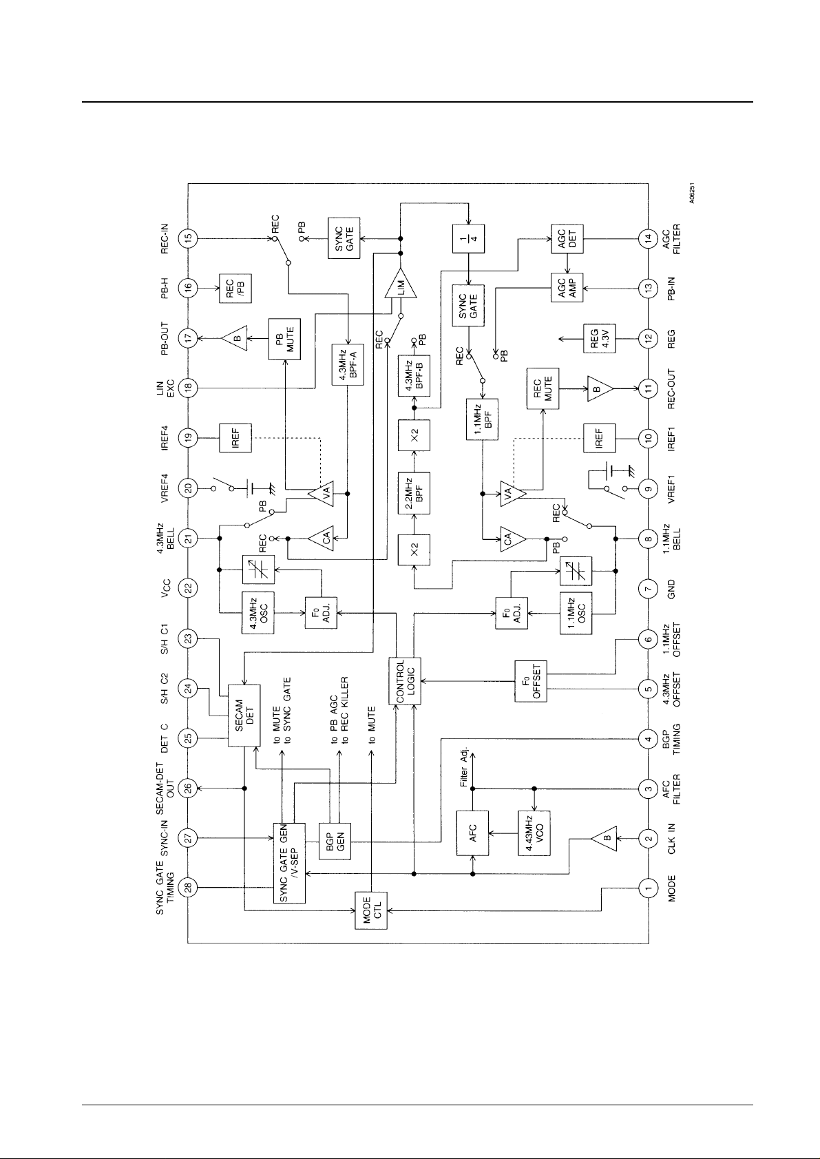
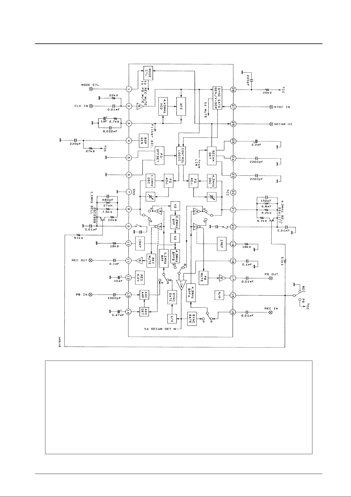
Block Diagram
No. 5288-5/7
LA7337
Page 6

No. 5288-6/7
LA7337
Test Circuit Diagram
Note: Use an FET probe when measuring T8, T21, and BGP.
Page 7
No. 5288-7/7
LA7337
This catalog provides information as of January, 1997. Specifications and information herein are subject to
change without notice.
■ No products described or contained herein are intended for use in surgical implants, life-support systems, aerospace
equipment, nuclear power control systems, vehicles, disaster/crime-prevention equipment and the like, the failure of
which may directly or indirectly cause injury, death or property loss.
■ Anyone purchasing any products described or contained herein for an above-mentioned use shall:
➀
Accept full responsibility and indemnify and defend SANYO ELECTRIC CO., LTD., its affiliates, subsidiaries and
distributors and all their officers and employees, jointly and severally, against any and all claims and litigation and all
damages, cost and expenses associated with such use:
➁
Not impose any responsibility for any fault or negligence which may be cited in any such claim or litigation on
SANYO ELECTRIC CO., LTD., its affiliates, subsidiaries and distributors or any of their officers and employees
jointly or severally.
■ Information (including circuit diagrams and circuit parameters) herein is for example only; it is not guaranteed for
volume production. SANYO believes information herein is accurate and reliable, but no guarantees are made or implied
regarding its use or any infringements of intellectual property rights or other rights of third parties.
Test Circuit Diagram
 Loading...