

Page 1
Parameter Symbol Conditions Ratings Unit
Maximum supply voltage V
CC
max 14 V
Pin 2 input voltage V
IN
2DC ±45 Vp-p
Pin 2 input current I
IN
2 ±1.5 mA
Allowable power dissipation Pd max Ta ≤ 65 °C 500 mW
Operating temperature Topr –10 to +65 °C
Storage temperature Tstg –55 to +150 °C
Ordering number : EN5642
43097HA(OT) No. 5642-1/11
Overview
The LA7289 includes on chip all functions required for
the record and playback of VCR audio signals and
achieves complete adjustment-free operation by the
adoption of an automatic record bias current adjustment
circuit. In addition, the inclusion of a switching circuit for
switching between tuner and line input in addition to the
circuits provided by earlier ICs makes the LA7289 truly
optimal for audio VCR products.
Functions
• Equalizer amplifier
• Ripple filter
• Record/playback switching circuit
• Muting
• SP/LP/EP switching circuit
• Record amplifier
• ALC
• Tape head switching circuit
• Automatic record bias adjustment circuit
• Input switching circuit (line/tuner)
Features
• Adjustment-free record bias current (automatic
adjustment circuit adopted)
• Built-in record bias oscillator circuit power supply
switch
• Record equalizer choke coil no longer required
• Playback amplifier input noise voltage: 1.0 µV rms
• Value of the ALC detector capacitor reduced (to 3.3 µF)
• Built-in high-voltage head switching circuit
• Supply voltage: supports both 9 and 12-V operation
• Built-in input switching circuit (for the line and tuner
inputs)
Package Dimensions
unit: mm
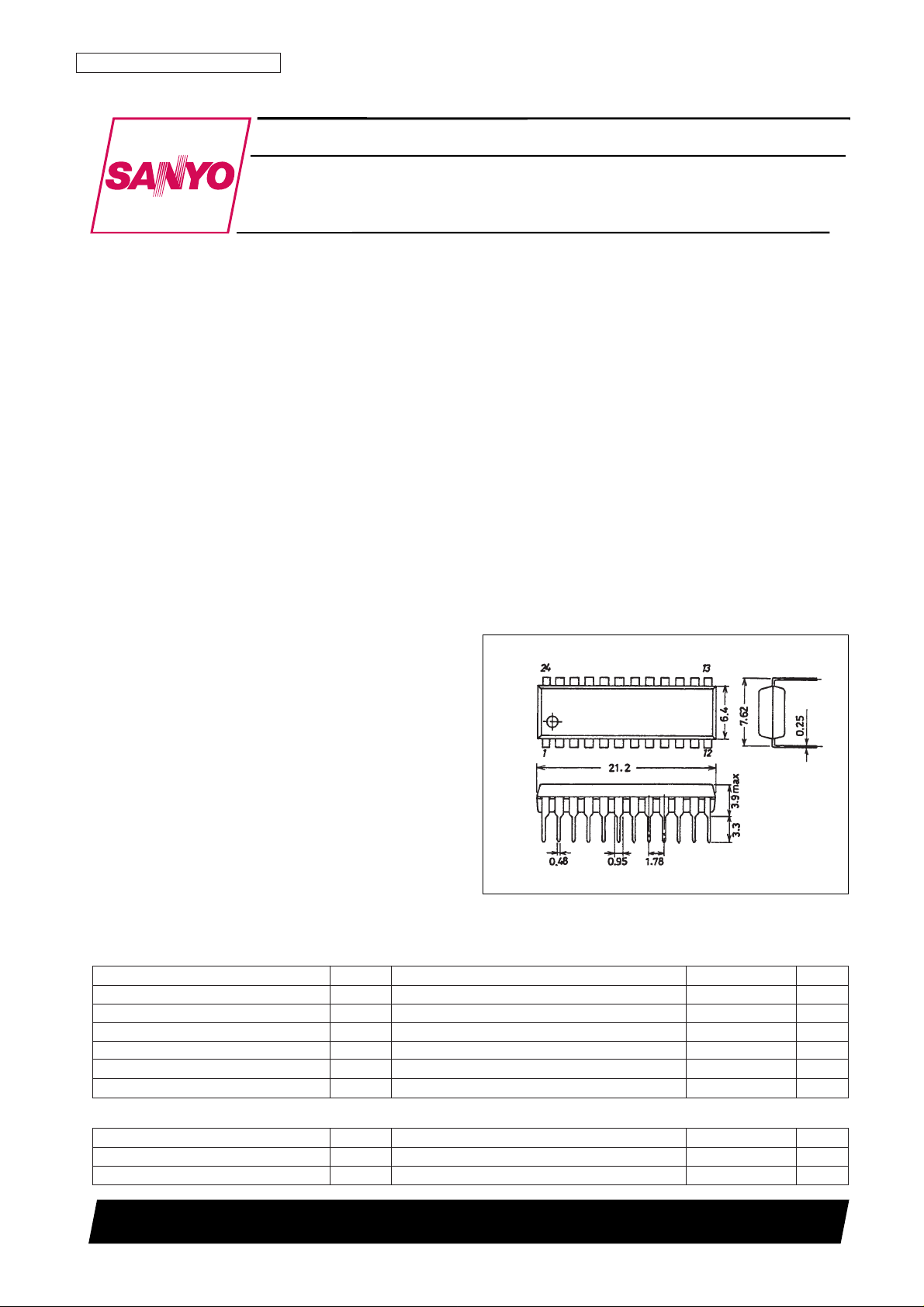
3067-DIP24S
SANYO: DIP24S
[LA7289]
LA7289
SANYO Electric Co.,Ltd. Semiconductor Bussiness Headquarters
TOKYO OFFICE Tokyo Bldg., 1-10, 1 Chome, Ueno, Taito-ku, TOKYO, 110 JAPAN
VCR Audio Signal Record and Playback Processor
Monolithic Linear IC
Specifications
Maximum Ratings at Ta = 25°C
Parameter Symbol Conditions Ratings Unit
Recommended supply voltage V
CC
9, 12 V
Allowable operating voltage range V
CC
op 8.5 to 12.5 V
Operating Conditions at Ta = 25°C
Page 2
No. 5642-2/11
LA7289
Parameter Symbol Conditions
Ratings
Unit
min typ max
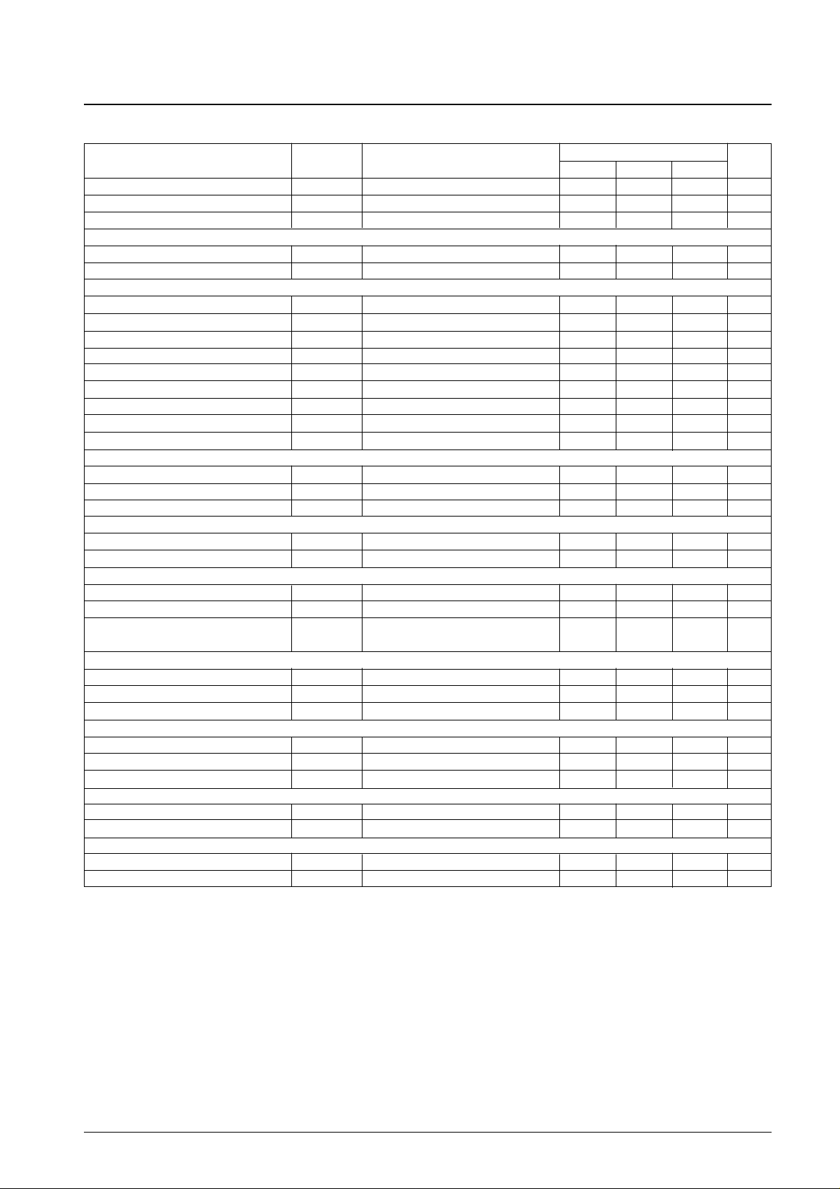
Current drain (EE) I
CCE
No signal 10.0 12.5 15.0 mA
Current drain (playback) I
CCP
No signal 11.2 14.0 16.8 mA
Current drain (record) I
CCR
No signal 9.6 12.0 14.4 mA
[Equalizer amplifier]
Open-circuit voltage gain VG
OE
VO= –6dBV 58.4 64.4 – dB
Input noise voltage V
NIE
Rg = 620 Ω, DIN audio filter – 1.0 1.8 µVrms
[Line Amplifier]
Voltage gain (PB input) VG
LP
VO= –6dBV 20.1 20.6 21.1 dB
Voltage gain (LINE input) VG
LL
VO= –6dBV 20.1 20.6 21.1 dB
Voltage gain (TUNER input) VG
LT
VO= –6dBV 20.1 20.6 21.1 dB
Harmonic distortion THD
L
VO= –6dBV – 0.05 0.3 %
Output noise voltage V
NOL
Rg = 620 Ω, DIN audio filter – –75 –69 dBV
Maximum output voltage V
OML
THD = 1% 1.7 2.5 – Vrms
Output voltage when ALC operating V
OA
VIN= –25dBV –7 –6 –5 dBV
ALC effect ALC V
IN
= –25dBV to –5dBV – 1 3 dB
Total harmonic distortion when ALC operating
THD
A
VIN= –25dBV – 0.05 0.6 %
[Record Amplifier]
Voltage gain VG
CR
VO= –6dBV 13.5 14.0 14.5 dB
Harmonic distortion THD
R
VO= –6dBV – 0.05 0.3 %
Maximum output voltage V
OMR
THD = 1% 1.7 2.5 – Vrms
[REC/EE Switching Circuit]
Record mode hold voltage V
RR
The pin 19 DC voltage 3.6 – 6.0 V
EE mode hold voltage V
RE
The pin 19 DC voltage 0 – 1 V
[Muting Circuit]
On state hold voltage V
MON
The pin 18 DC voltage 3.6 – 6.0 V
Off state hold voltage V
MOFF
The pin 18 DC voltage 0 – 1 V
Muting attenuation
M
P
, ML, M
T
80 90 – dB
(PB, LINE. TUNER)
[PB, LINE. TUNER Switching Circuit]
PB mode hold voltage V
LP
The pin 17 DC voltage 3.6 – 6.0 V
LINE mode hold voltage V
LL
The pin 17 DC voltage 1.8 – 2.6 V
TUNER mode hold voltage V
LT
The pin 17 DC voltage 0 – 1.0 V
[EP. LP. SP Switching Circuit]
EP mode hold voltage V
EE
The pin 16 DC voltage 3.6 – 6.0 V
LP mode hold voltage V
EL
The pin 16 DC voltage 1.8 – 2.6 V
SP mode hold voltage V
EE
The pin 16 DC voltage 0 – 0.8 V
[Switching Circuit]
Pin 2 on resistance R
ON
2 I1 = ±1 mA – 10 30 Ω
Pin 2 input voltage V
IN
2 Ta = 65°C, f = 70 kHz (sin), ILK= 10 µA – – ±45 V
[Record Bias Automatic Adjustment Circuit]
Record bias current I
B
220 245 270 µA
Pin 1 output control range V1 2.0 4.0 6.0 V
Electrical Characteristics at Ta = 25°C, VCC= 12 V, f = 1 kHz, 0 dBV = 1.0 Vrms
Page 3
No. 5642-3/11
LA7289
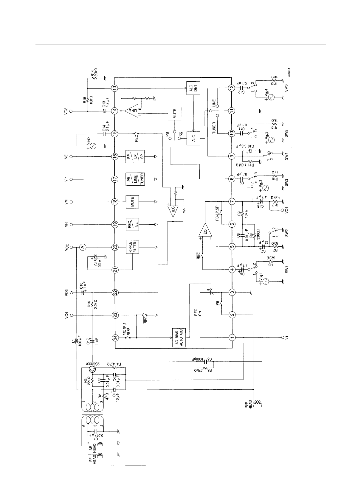
Test Circuit
Page 4
No. 5642-4/11
LA7289
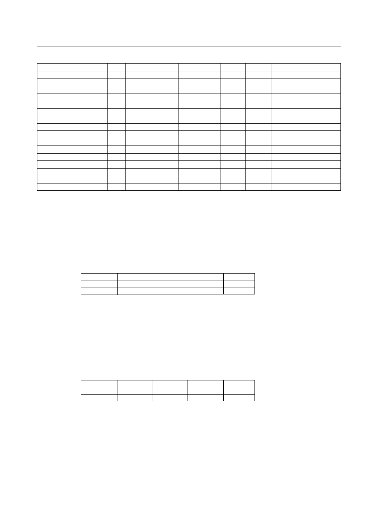
Switching Operations
Test item (signal) SW1 SW2 SW3 SW4 SW5 SW6 V
M
V
P
V
R
Input Measurement
I
CCE
2 1 3 2 2 2 GND GND GND - I
O
I
CCP
2 1 3 2 2 2 GND 5 V GND - I
O
I
CCR
2 1 3 2 2 2 GND GND 5 V - I
O
VG
OE
1 2 3 2 2 2 GND 5 V GND VIN1 VO1
V
NIE
2 1 3 2 2 2 GND 5 V GND - VO1
VG
LP
, THDL, V
OML
2 1 2 2 2 2 GND 5 V GND VIN2 VO2
VG
LL
2 1 3 2 2 1 GND 2 V GND VIN4 VO2
VG
LT
2 1 3 2 1 2 GND GND GND VIN3 VO2
V
NOL
2 1 3 2 2 2 GND GND GND - VO2
V
OA
, ALC, THD
A
2 1 3 1 1 2 GND GND GND VIN3 VO2
VG
CR
, THDR, V
OMR
2 1 3 2 2 2 GND GND 5 V VIN5 VO3
M
P
1 1 1 2 2 2 5 V 5 V GND VIN1 VO2
M
L
2 1 3 2 2 1 5 V 2 V GND VIN4 VO2
M
T
2 1 3 2 1 2 5 V GND GND VIN3 VO2
I
B
2 1 1 2 2 2 GND GND 5 V - VO4
V1 2 1 1 2 2 2 GND GND 5 V - V1
Head Coil Specifications
1. Application circuit 1 (Series erase head type)
• R/P Head 58 kΩ ± 15 % (f = 70 kHz)
• AE Head 34 Ω ± 20 % (f = 70 kHz)
• FE Head 80 Ω ± 15 % (f = 70 kHz)
• Oscillator coil test number: 15419A, Model no. 7QM3
2 Application circuit 2 (Parallel erase head type)
• R/P Head 58 kΩ ± 15 % (f = 70 kHz)
• AE Head 180 Ω ± 20 % (f = 70 kHz)
• FE Head 80 Ω ± 15 % (f = 70 kHz)
• Oscillator coil test number: 15415A, Model no. 7QM3
For more information contact: Tokyo Parts Industries Co., Ltd.
Telephone: +81-270-25-1191
Pin No. 3 - 2 2 - 1 6 - 5 5 - 4
Line type 2UEW-0.09 2UEW-0.09 2UEW-0.09 2UEW-0.09
Total windings 32T 20T 176T 29T
Pin No. 3 - 2 2 - 1 4 - 5 5 - 6
Line type 2UEW-0.10 2UEW-0.10 2UEW-0.10 2UEW-0.10
Total windings 10T 22T 104T 22T
Page 5
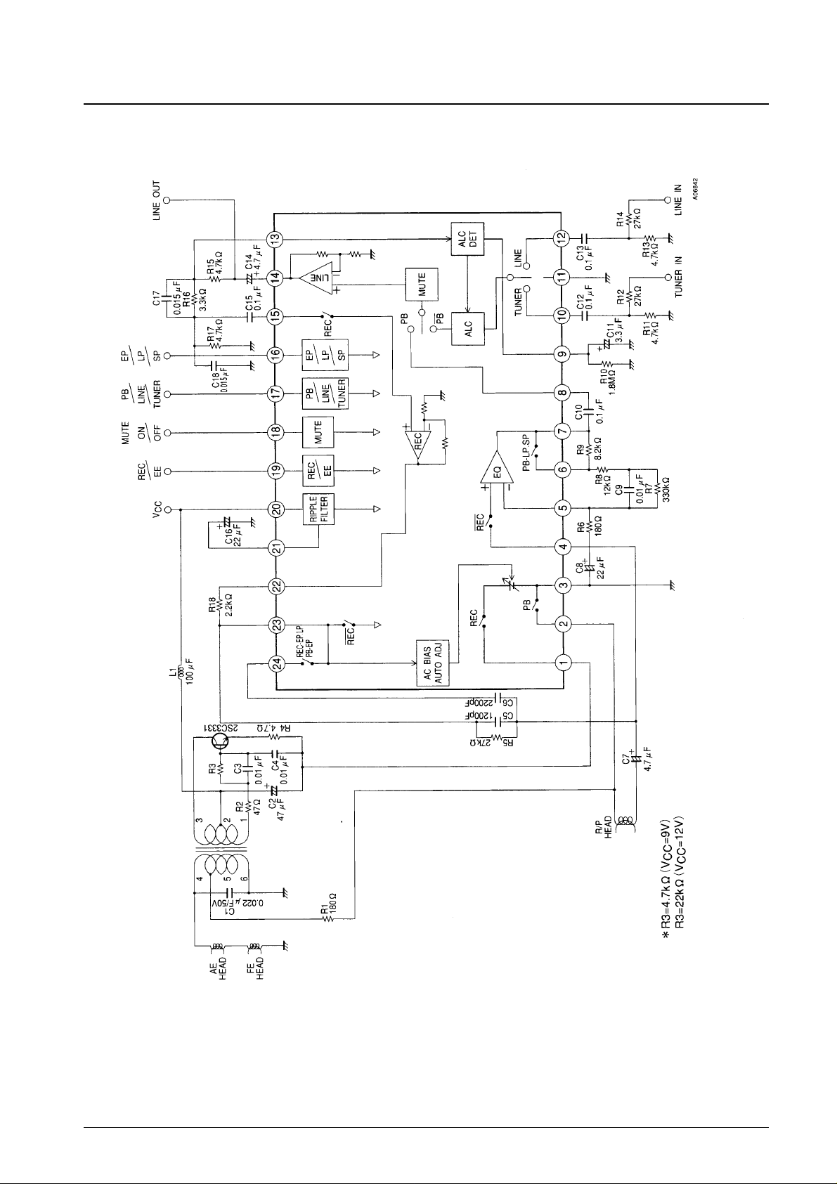
No. 5642-5/11
LA7289
Application circuit 1 (Series erase head type)
Page 6
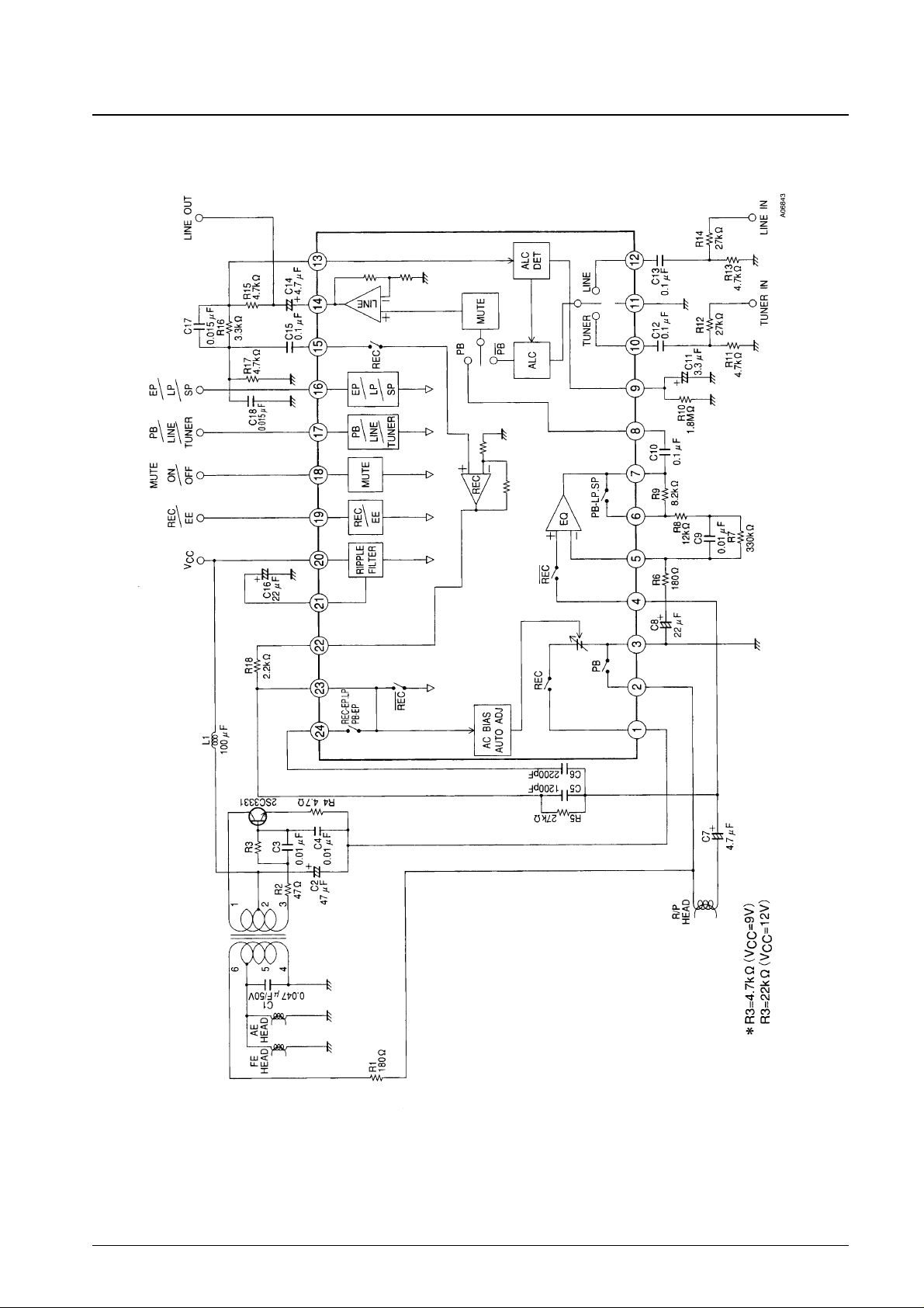
No. 5642-6/11
LA7289
Application Circuit 2 (Parallel erase head type)
Page 7
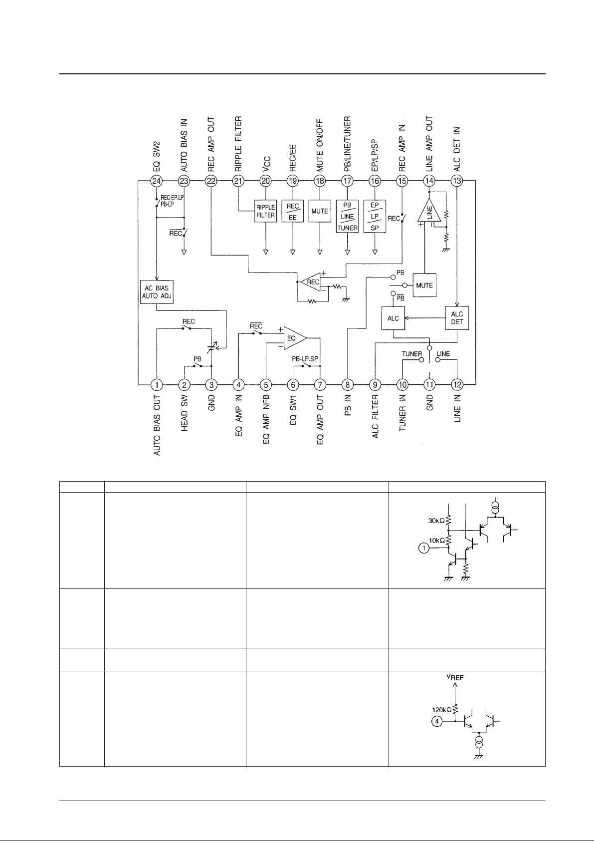
No. 5642-7/11
LA7289
Block Diagram
Pin No. Function Function description Internal circuit
1 Record bias automatic control output EE, playback → V
CC
Record → Control voltage
2 Head switch (high voltage) Playback → On
Record, EE → Off
On resistance → 10 Ω (typical)
Withstand voltage when off
→ ±45 V (f = 70 kHz)
3 GND Ground used for the pin 2 head
switching circuit and the EQ amplifier.
4 EQ amplifier input Inputs the playback from the head
with an input impedance of
120 kΩ (typical).
Pin Functions
Continued on the next page.
A06818
A06819
Page 8
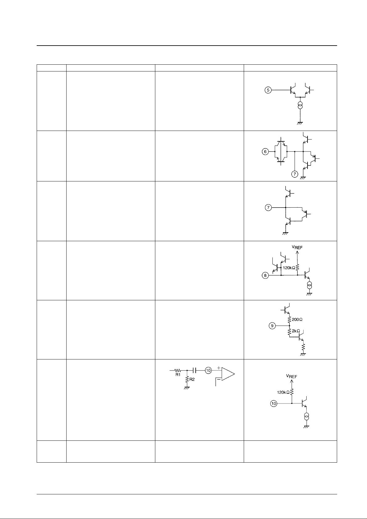
Pin No. Function Function description Internal circuit
5 EQ AMP NFB Negative feedback for the EQ amplifier.
6 EQ switch 1 Switches the playback EQ amplifier
high-frequency voltage gain.
LP, SP → On
EP → Off
On resistance → 20 Ω (typical)
7 EQ amplifier output Output impedance →50 Ω(typical)
8 Line amplifier playback input Inputs the playback signal from
the EP amplifier. Since pin 8 has
the high input impedance of 120 kΩ,
a 0.1 µF ceramic capacitor can be used
as the coupling capacitor.
9 ALC FILTER Detection is performed using the
capacitor connected between this pin
and ground. The attack and recovery times
are determined by the time constant of
the RC circuit connected to this pin.
10 Line amplifier tuner input Inputs the EE and record signal.
The reference input is set by the resistors
R1 and R2. The amplifier gain is fixed
at 21.0 dB. Since pin 10 has the high input
impedance of 120 kΩ, a 0.1 µF ceramic
capacitor can be used as the coupling
capacitor.
11 GND Ground for all the circuit blocks except
the pin 2 head switching circuit and the
EQ amplifier.
No. 5642-8/11
LA7289
Continued from the preceding page.
Continued on the next page.
A06820
A06821
A06822
A06823
A06824
A06825
A06826
Page 9
No. 5642-9/11
LA7289
Continued from the preceding page.
Continued on the next page.
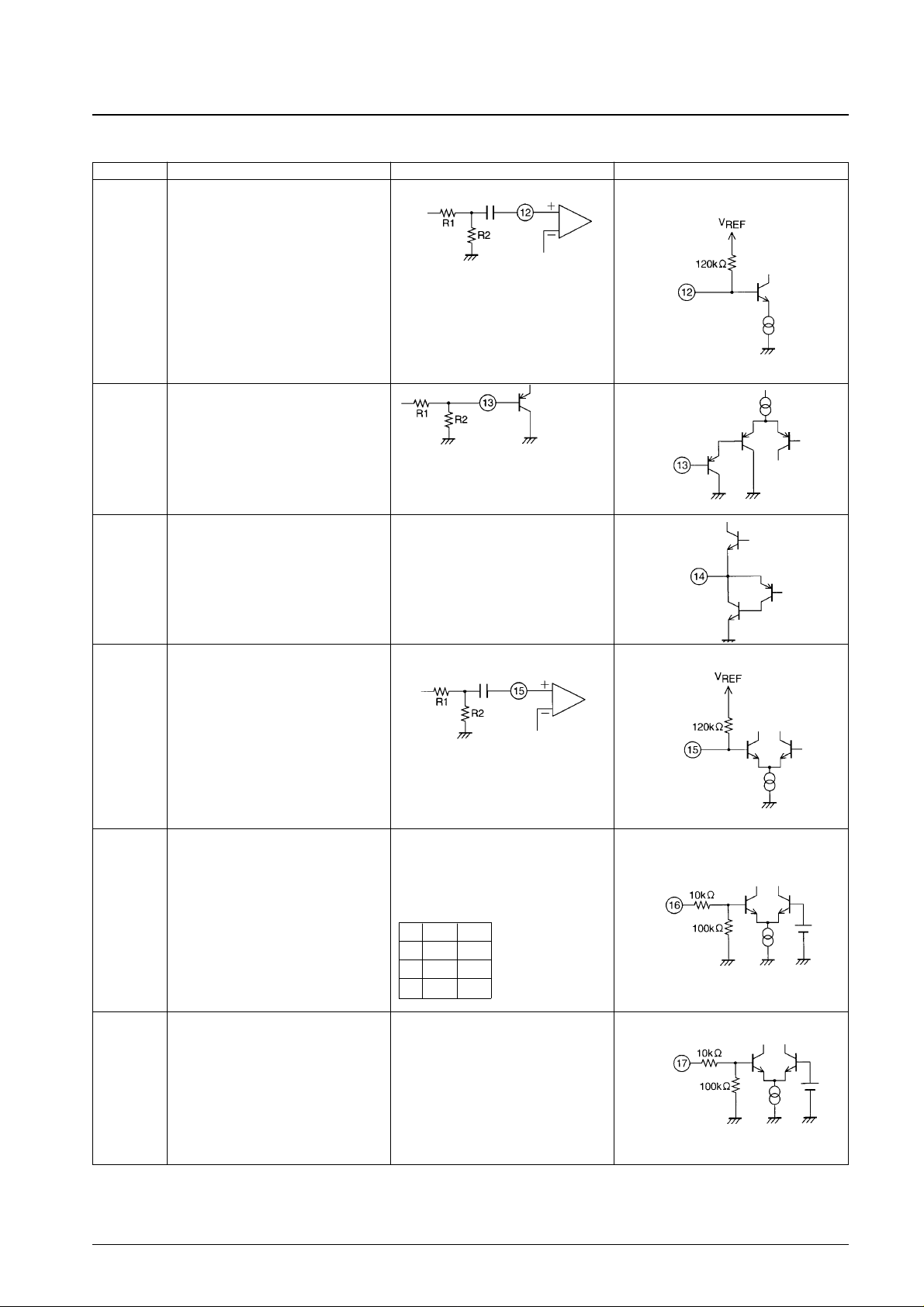
Pin No. Function Function description Internal circuit
12 Line amplifier line input Inputs the EE and record signals.
The reference input is set by the resistors
R1 and R2. The amplifier gain is fixed at
21.0 dB. Since pin 12 has the high input
impedance of 120 kΩ, a 0.1 µF ceramic
capacitor can be used as the coupling
capacitor.
13 ALC detector input
Inputs the line amplifier output signal.
The ALC level is determined by
the resistors R1 and R2.
14 Line amplifier output Output impedance → 50 Ω (typical)
15 Record amplifier input Inputs the record signal from the line
amplifier.
The record current is set by the resistors
R1 and R2. Since pin 15 has the high input
impedance of 120 kΩ, a 0.1 µF ceramic
capacitor can be used as the coupling
capacitor.
16 EP/LP/SP control If the pin 16 voltage is:
3.0 to 6.0 V: EP mode
1.8 to 2.6 V: LP mode
0.0 to 0.8 V: SP mode.
Switch on state pin numbers:
REC PB
EP 24 24
LP 24, 6 6
SP 6 6
17 PB/LINE/TUNER control If the pin 17 voltage is:
3.6 to 6.0 V: PB mode
1.8 to 2.6 V: LINE mode
0.0 to 1.0 V: TUNER mode.
A06827
A06829
A06831
A06832
A06834
A06835
A06833
A06830
A06828
Page 10
No. 5642-10/11
LA7289
Continued from the preceding page.
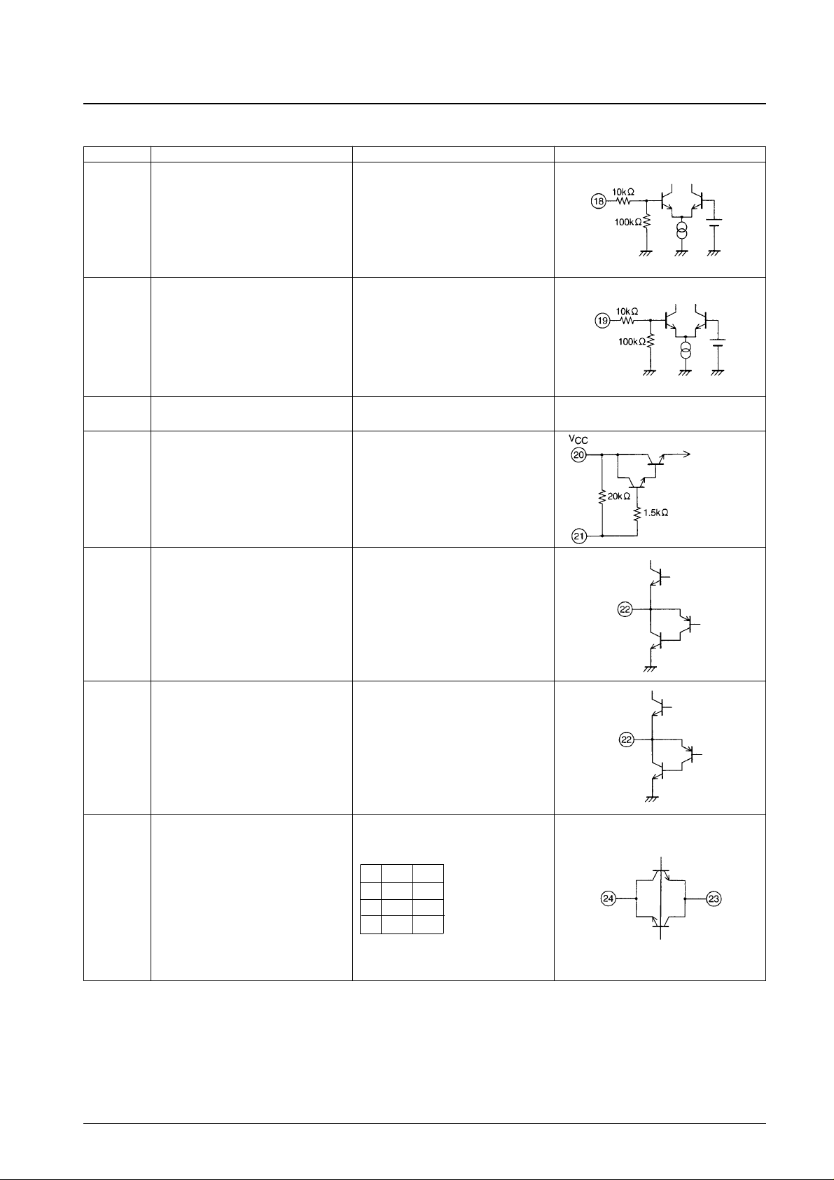
Pin No. Function Function description Internal circuit
18 Muting control When the pin 18 voltage is:
3.6 to 6.0 V: Muting will be on.
0.0 to 1.5 V: Muting will be off.
19 Record/EE control When the pin 19 voltage is:
3.0 to 6.0 V: Record mode
0.0 to 1.0 V: EE mode
20 Power supply (V
CC
) VCCmax = 14 V
V
CC
= 8.5 V to 12.5 V
21 Ripple filter Connect an electrolytic capacitor between
this pin and ground to remove ripple
from the power supply.
22 Record amplifier output Output impedance → 50 Ω (typical)
23 Record bias automatic control input EE and playback modes → On
and playback switch Record mode → Off
On resistance → 20 Ω (typical)
24 EQ switch 2 This pin switches the high-band peaking
frequency in record and playback modes.
REC PB
EP On On
LP On Off
SP Off Off
On resistance: 30 Ω (typical)
Power supply
for all circuit
blocks
A06836
A06837
A06838
A06839
A06840
A06841
Page 11

No. 5642-11/11
LA7289
This catalog provides information as of April, 1997. Specifications and information herein are subject to change
without notice.
■ No products described or contained herein are intended for use in surgical implants, life-support systems, aerospace
equipment, nuclear power control systems, vehicles, disaster/crime-prevention equipment and the like, the failure of
which may directly or indirectly cause injury, death or property loss.
■ Anyone purchasing any products described or contained herein for an above-mentioned use shall:
➀ Accept full responsibility and indemnify and defend SANYO ELECTRIC CO., LTD., its affiliates, subsidiaries and
distributors and all their officers and employees, jointly and severally, against any and all claims and litigation and all
damages, cost and expenses associated with such use:
➁ Not impose any responsibility for any fault or negligence which may be cited in any such claim or litigation on
SANYO ELECTRIC CO., LTD., its affiliates, subsidiaries and distributors or any of their officers and employees
jointly or severally.
■ Information (including circuit diagrams and circuit parameters) herein is for example only; it is not guaranteed for
volume production. SANYO believes information herein is accurate and reliable, but no guarantees are made or implied
regarding its use or any infringements of intellectual property rights or other rights of third parties.
 Loading...