

Page 1
SANYO Electric Co.,Ltd. Semiconductor Bussiness Headquaters
TOKYO OFFICE Tokyo Bldg., 1-10, 1 Chome, Ueno, Taito-ku, TOKYO, 110-8534 JAPAN
VCR Audio Signal Recording
and Playback Processor
Ordering number:EN4091
LA7285, 7285M
Monolithic Linear IC
Overview
The LA7285 and LA7285M include on chip all functions
required for the record and playback of VCR audio
signals. In addition, the inclusion of a switching circuit
for switching between tuner and line input in addition to
the circuits provided by earlier ICs makes the LA7285
truly optimal for audio VCR products.
Funtions
• Equalizer amplifier
• Line amplifier
• Recording/playback switch
• Recording amplifier
• Mute
• SP, LP, EP switch
• Ripple filter
• ALC
• Tape head switch
• Line/tuner input switch
Features
• Built-in input switching circuit (for the line and tuner
inputs).
• Smaller package leaves large space for other
components.
• Equalizer input/output capacitors not required.
• Low gain variation eliminates the need for external
ajustment.
• Supply voltage : 9V and 12V operation.
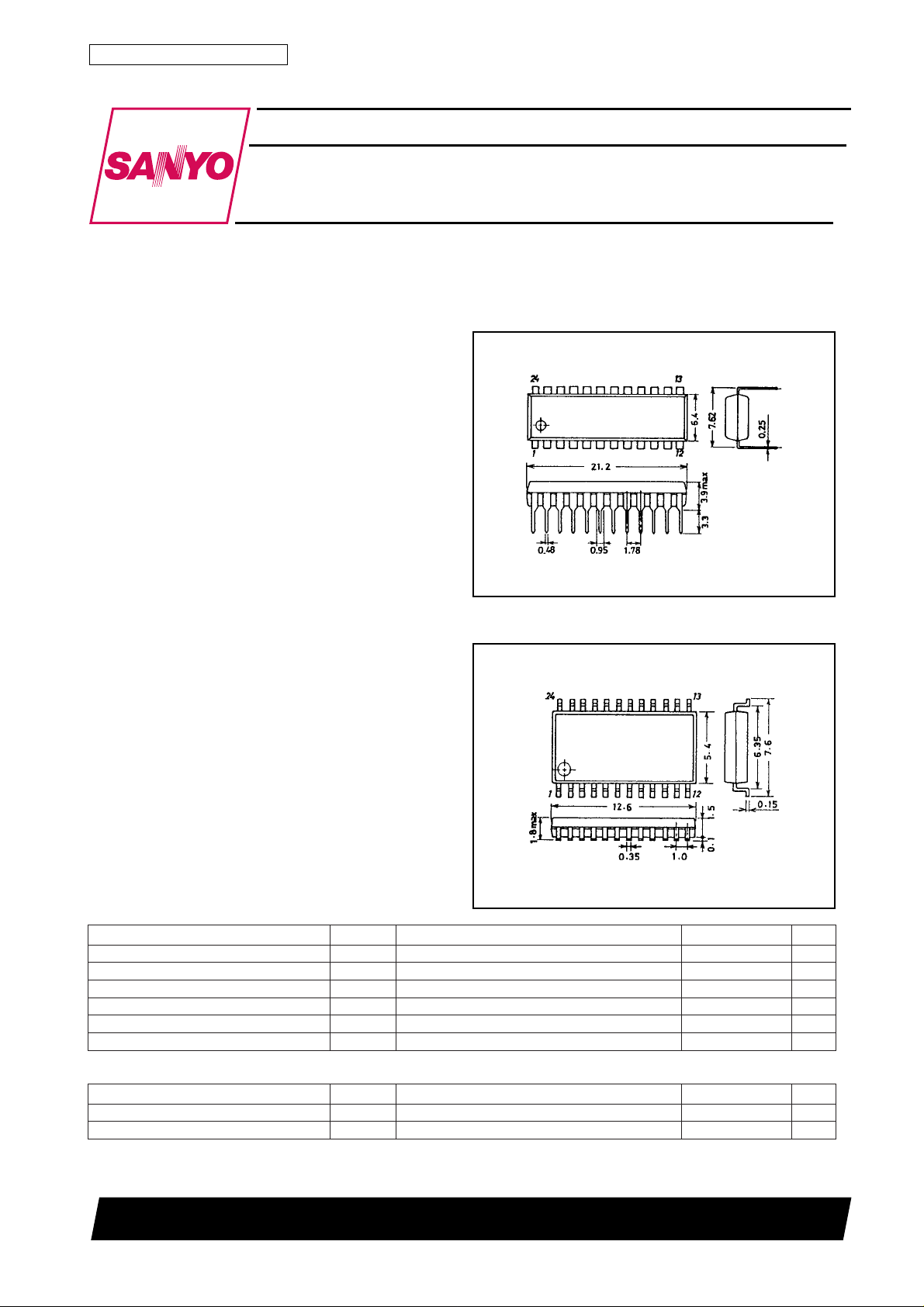
Package Dimensions
unit:mm
3067-DIP24S
[LA7285]
unit:mm
3112-MFP24S
[LA7285M]
SANYO:DIP24S
Specifications
Maximum Ratings at Ta = 25˚C
retemaraPlobmySsnoitidnoCsgnitaRtinU
egatlovylppusmumixaMV
egatlovtupni1niPV
tnerructupni1niPV
noitapissidrewopelbawollAxamdP 004Wm
erutarepmetgnitarepOrpoT 56+ot01–
erurtarepmetegarotSgtsT 051+ot55–
xam 41V
CC
1CD 56+p-pV
NI
1 5.1±Am
NI
Ta≤65˚C
Operating Conditions at Ta=25˚C
retemaraPlobmySsnoitidnoCsgnitaRtinU
egatlovylppusdednemmoceRV
egnaregatlovylppusgnitarepOV
CC
po 57.21ot5.8V
CC
53098HA (KT) No.4091-1/7
SANYO:MFP24S
˚C
˚C
21V
Page 2
LA7285, 7285M
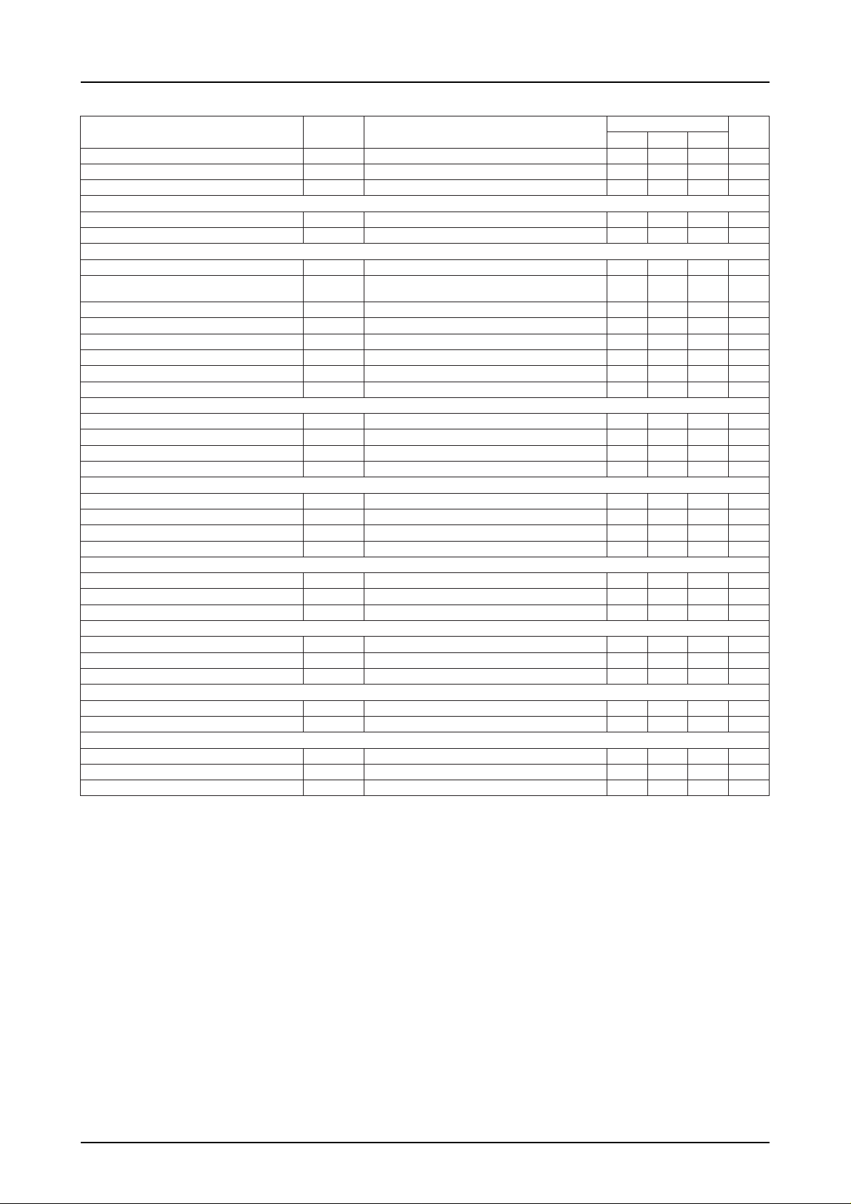
Operating Characteristics at Ta=25˚C, VCC=12V, f=1kHz, 0dBV : 1.0 Vrms
retemaraPlobmySsnoitidnoC
)EE(noitpmusnoctnerruCI
)BP(noitpmusnoctnerruCI
)CER(noitpmusnoctnerruCI
]reifilpmarezilauqE[
niagegatlovtiucric-nepOGV
egatlovesiontupnitnelaviuqEV
]reifilpmaeniL[
)tupniBP(niagegatloVGV
)tupniENIL,EE(niagegatloV
noitrotsidcinomrahlatoTDHT
egatlovesiontuptuOV
egatlovtuptuomumixaMV
nosiCLAnehwegatlovtuptuOV
tceffeCLACLAV
nosiCLAnehwnoitrotsiDDHT
]reifilpmagnidroceR[
)nepo(niagegatloVGV
)esloc(niagegatloVGV
noitrotsidcinomrahlatoTDHT
egatlovtuptuomumixaMV
]tiucricetuM[
egatlovnOV
egatlovffOV
)EE,BP(noitaunettaetuMM
)CER(noitaunettaetuMM
]tiucrichctiwsPS,PL,PE[
egatlovdlohedomPEV
egatlovdlohedomPLV
egatlovdlohedomPSV
]tiucrichctiwsBPrenuT/eniL[
egatlovdlohedomeniLV
egatlovdlohedomrenuTV
egatlovdlohedomBPV
]tiucrichctiwsEE,CER[
egatlovdlohedomCERV
egatlovdlohedomEEV
]hctiwStceleSdaeH[
ecnatsiserno1niPR
ecnatsiserno2niPR
egatlovtupni2niPV
ECC
PCC
RCC
EO
EIN
PL
GV
,EL
GV
LL
LVO
LON
LMO
AO
A
RO
RO
RVO
RMO
NOM
FFOM
PM,E
R
EE
LE
SE
LL
TL
PL
RR
ER
1Am1±=1I0203
NO
2Am1±=2I501
NO
1 54±V
NI
langisoN5.90.315.61Am
langisoN5.90.315.61Am
langisoN0.80.110.41Am
V
V
V
V
V
V
V
VBd7–=0.660.17Bd
O
k2.2=gR Ω retlifoiduANID,2.18.1smrVµ
VBd7–=0.125.120.22Bd
O
VBd7–=0.125.120.22Bd
O
VBd7–=50.03.0%
k2.2=gR Ω retlifoiduANID,27–66–VBd
%1=DHT5.11.2smrV
VBd72–=0.8–0.7–0.6–VBd
NI
NI
VBd72–=50.06.0%
NI
VBd7–=0.740.25Bd
O
VBd7–=5.210.315.31Bd
O
VBd7–=1.03.0%
%1=DHT5.10.2smrV
VBd7–otVBd72–=0.10.3Bd
egatlovCD32niP5.20.6V
egatlovCD32niP05.1V
egatlovCD12niP6.30.6V
egatlovCD12niP8.16.2V
egatlovCD12niP00.1V
egatlovCD22niP6.30.6V
egatlovCD22niP8.16.2V
egatlovCD22niP00.1V
egatlovCD42niP3V
egatlovCD42niP00.1V
Ta=65˚C, f=80kHz (sin), ILK=10µA
sgnitaR
nimpytxam
0809Bd
5657Bd
CC
tinU
V
Ω
Ω
No.4091-2/7
Page 3
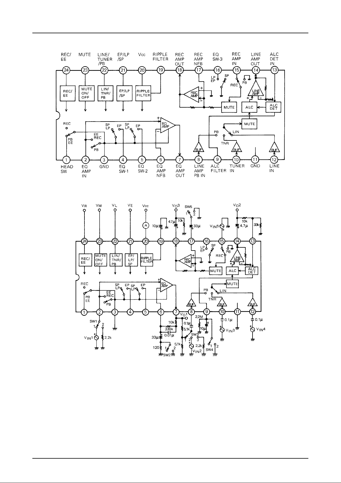
Block Diagram
Test Circuit
LA7285, 7285M
Unit (resistance:Ω, capacitance:F)
No.4091-3/7
Page 4
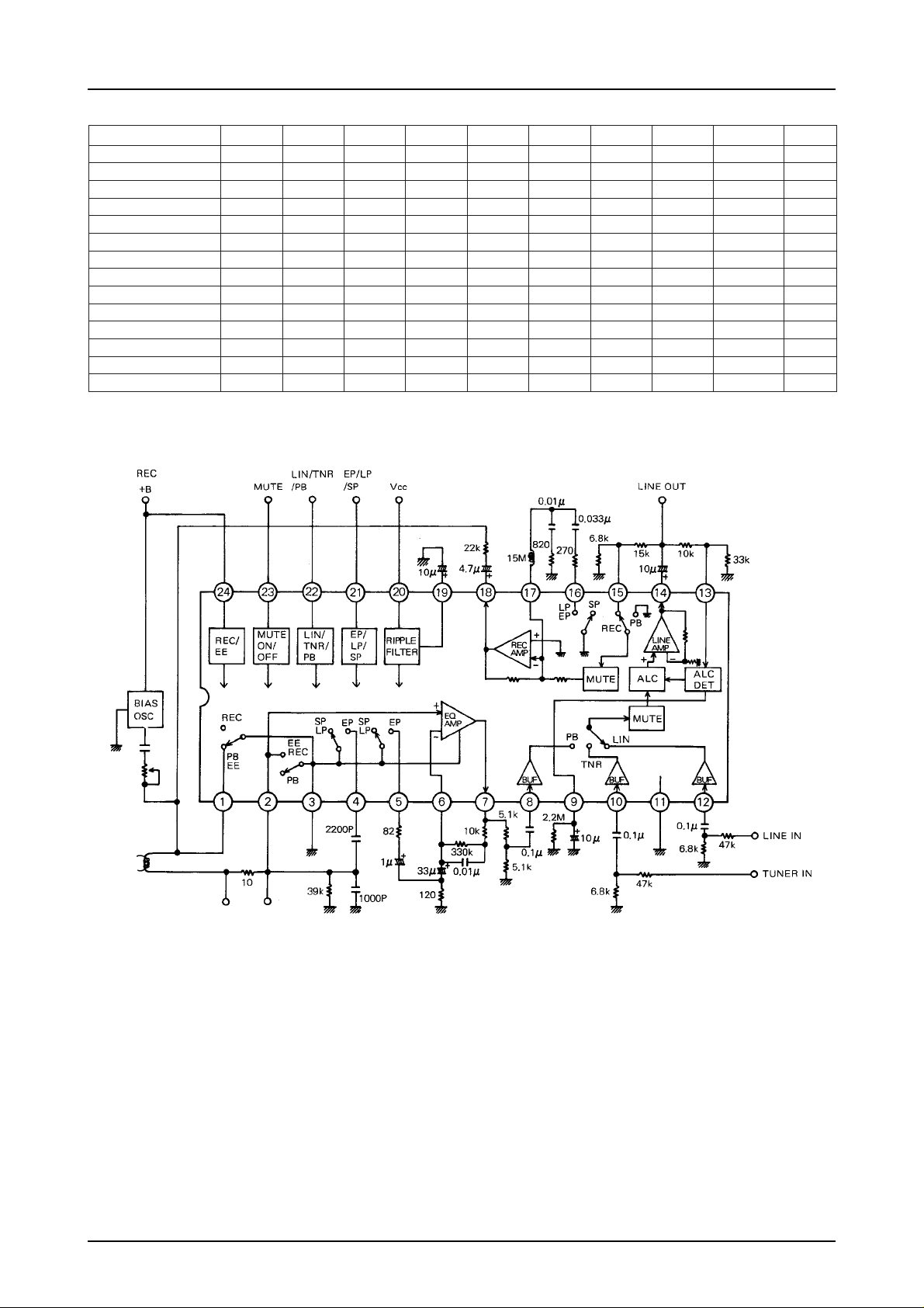
Switch Operation Table
)lobmys(metitseT1WS2WS3WS4WS5WSVMV
I
ECC
I
PCC
I
RCC
GV
EO
V
EIN
GV
DHT,
PL
GV
EL
V
V
AO
GV
OGV
M
P
M
R
M
E
V,
L
LL
DHT,
RV,RMO
LMO
DHT,CLA,
A
GV,
LON
RO
R
21121 DNGV5DNG–A
21121 DNGDNGDNG–A
21121 DNGV5V5–A
12321 DNGDNGDNGV
21321 DNGDNGDNG–V
21221 DNGDNGDNGV
21121 DNGV5,V5.2DNGVNIV,3NI4VO2
21321 DNGV5DNG–V
21311 DNGV5,V5.2DNGVNIV,3NI4VO2
21322 DNGV5DNGV
21321 DNGV5DNGV
11121 V5DNGDNGV
21121 V5V5DNGV
21321 V5V5DNGV
Sample Application Circuit
LA7285, 7285M
L
V
R
tupnIerusaeM
1VO1
NI
2VO2
NI
5VO3
NI
5VO3
NI
1VO2
NI
5VO3
NI
2VO2
NI
1
O
2
O
Unit (resistance:Ω, capacitance:F)
No.4091-4/7
Page 5
LA7285, 7285M
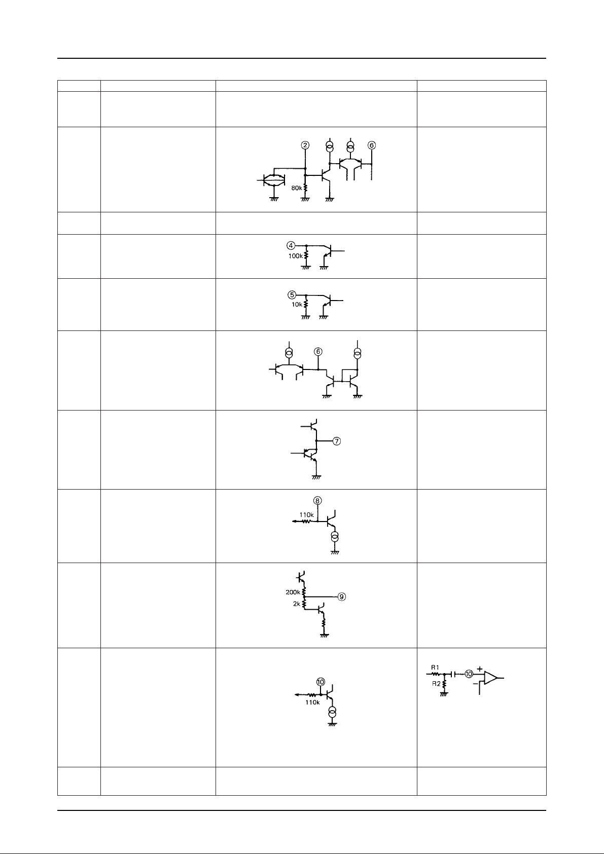
Pin Function
.oNniPemannoitcnuFniproftiucriclanretnI noitcnuffonoitpircseD
1
2
3DNG
41hctiwsedomPE
52hctiwsedomPE
Unit (resistance:Ω)
1hctiwsdaeH
)egatlovdnatshtiwhgih(
dnatupniPMAQE
2hctiwsdaeH
BP,EE → CER,ffo → ffo
ecnatsisernO → 02 Ω )pyt(
ffonehwegatlovdnatshtiW → V54±
)zHk08=f(
langiskcabyalprofecnadnepmitupnI
daehmorftupni → k08 Ω )pyt(
CER,EE → no
BP → ffo
ecnatsisernO → 5Ω )pyt(
dnahctiwsdaeh1niprofDNG
ylnoreifilpmArezilauqE
dnasdaehepategnahcotesU
.ycneuqerftnanoser
ecnatsisernO → 51 Ω )pyt(
ecnadnepmitupnI → k01 Ω )pyt(
)edomPE(
rezilauqEkcabyalPehtsehctiwS
ycneuqerfnoiger-hgihreifilpmA
.niagegatlov
ecnatatisernO → k51 Ω )pyt(
ecnadepmitupnI → k01 Ω )pyt(
)edomPE(
6BFNPMAQE
7tuptuoPMAQE
8tupniBPPMAENIL
9RETLIFCLA
Internal
reference
nipkcabdeef
evitagenreifilpmArezilauqE
ehtmorflangiskcabyalpehtstupnI
ehtesuaceB.reifilpmArezilauqE
K011sahgihsasiecnadepmitupni ,Ω
desuebnacroticapaccimarecFµ1.0a
.8nipnoroticapacgnilpuocehtrof
nehwdemrofrepsinoitcetedevaW
ahguorhtDNGotdetcennoc
dnakcattaeht,noitiddanI.roticapac
RdnaCybtessiemityrevocer
.stnatsnocemit
Inputs EE and REC signals.
01tupniRENUT
11DNG
Internal
reference
The reference input is set by resistors
R1 and R2.
The amplifier gain is fixed at 21.5dB.
In addition, because the input
impedance is as high as 110kΩ, a 0.1µF
ceramic capacitor can be used for the
coupling capacitor on pin 10.
ehttpecxeskcolbtiucricllarofDNG
.reifilpmArezilauqEdnahctiwsdaeh
Continued to next page.
No.4091-5/7
Page 6
LA7285, 7285M
Continued from proceeding page.
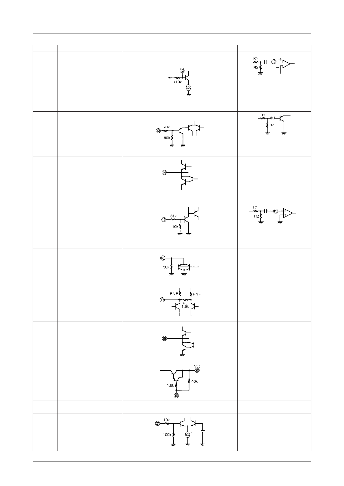
.oNniPemannoitcnuFniproftiucriclanretnI noitcnuffonoitpircseD
21tupniENIL
31noitcetedevawtupniCLA
41tuptuoPMAENIL
Unit (resistance:Ω)
Inputs EE and RE signals.
Internal
reference
The reference input is set by resistors
R1 and R2.The amplifier gain is fixed at
21.5 dB. In addition, because the input
impedance is as high as 110kΩ, a
0.1µF ceramic capacitor can be used
for the coupling capacitor on pin 12.
Inputs the Line Amplifier output
signal.
The ALC level is set by the resistors
R1 and R2.
Output inpedance → 50Ω (typ)
Inputs the recording signal from Line
Amplifier.
51tupniPMACER
61hctiwsedomPL
71BFNPMACER
81tuptuoPMACER
91retlifelppiR
Power supply of
each circuit block
The recording current is set by the
resistors R1 and R2. A coupling
capacitor is unnecessary as pin 15 is
a zero baias input.
Used to adjust the high-region peaking
frequency during recording amplifier in
LP mode.
On resistance → 15Ω (typ)
Intput inpedance → 50Ω (typ)
Recording amplifier negativefeedback input. Used to adjust the
high-region peaking frequency of the
recording amplifier with an L, C, R
network connected to ground.
Output inpedance → 40Ω (typ)
Ripple rejection is performed when
connected to GND through an
electrolytic capacitor for the filter.
02V(egatlovylppuS
12lortnoCPS/PL/PE
)
CC
VCC max=14V
VCC=8.5V to 12.75V
When the voltage on
pin 21 is 3.6V to 6.0V:EP;
when 1.8V to 2.6V:LP;
when 0V to 1.8V:SP
Switch On Pin Number
EP mode:4,5,16
LP mode:16
Continued to next page.
No.4091-6/7
Page 7
Continued from proceeding page.
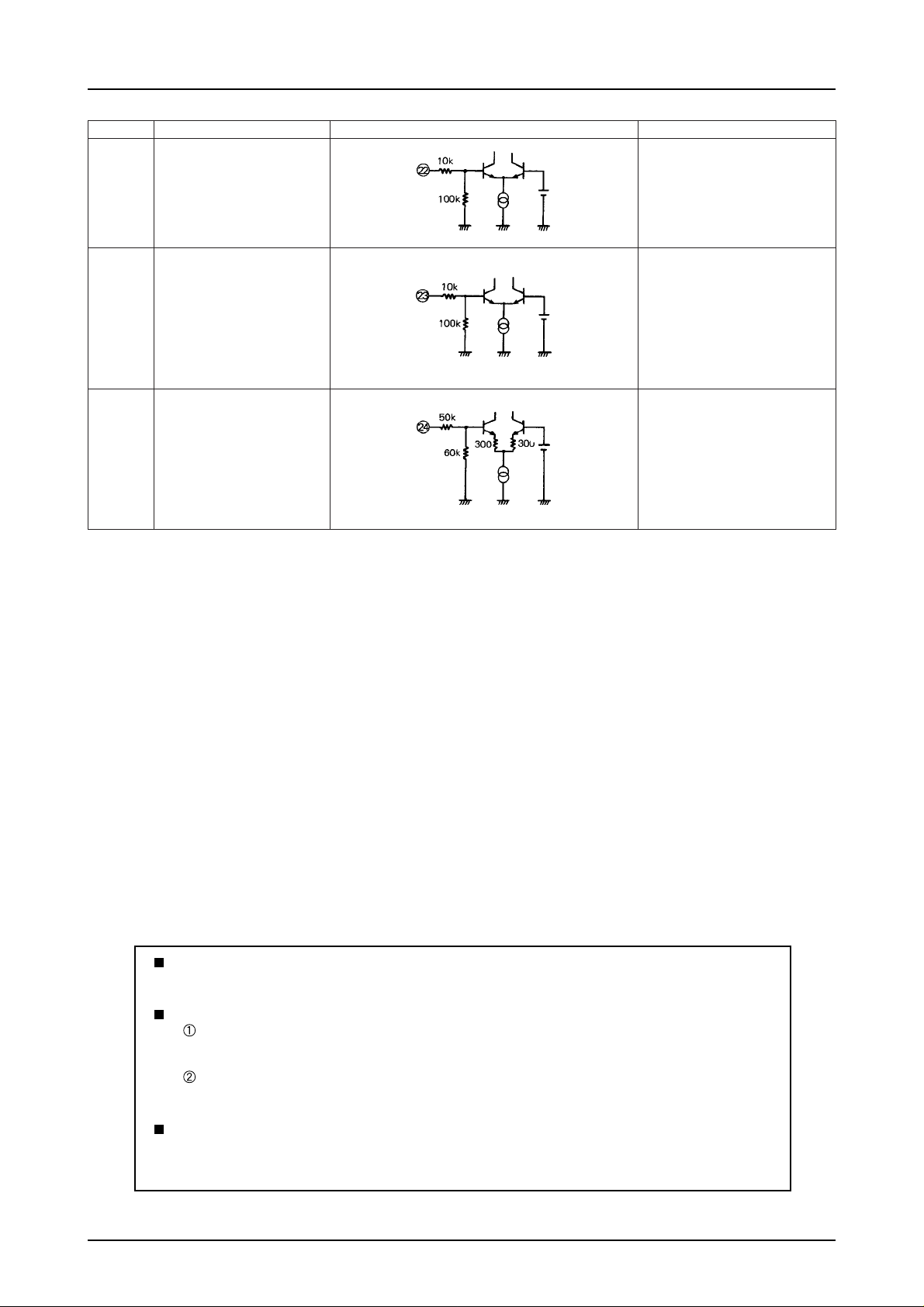
.oNniPemannoitcnuFniproftiucriclanretnI noitcnuffonoitpircseD
22lortnoCBP/RENUT/ENIL
LA7285, 7285M
Unit (resistance:Ω)
noegatlovehtnehW
;ENIL:V0.6otV6.3si22nip
RENUT:V6.2otV8.1nehw
BP:V0.1otV0nehw
32lortnoCETUM
42lortnoCEE/CER
noegatlovehtnehW
noegatlovehtnehW
VotV5.2si42nip
CC
EE:V0.1otV0nehw
;noETUM:V0.6otV5.2si32nip
ffoETUM:V5.1otV0nehw
;CER:
No products described or contained herein are intended for use in surgical implants, life-support systems,
aerospace equipment, nuclear power control systems, vehicles, disaster/crime-prevention equipment and
the like, the failure of which may directly or indirectly cause injury, death or property loss.
Anyone purchasing any products described or contained herein for an above-mentioned use shall:
Accept full responsibility and indemnify and defend SANYO ELECTRIC CO., LTD., its affiliates,
subsidiaries and distributors and all their officers and employees, jointly and severally, against any
and all claims and litigation and all damages, cost and expenses associated with such use:
Not impose any responsibilty for any fault or negligence which may be cited in any such claim or
litigation on SANYO ELECTRIC CO., LTD., its affiliates, subsidiaries and distributors or any of
their officers and employees jointly or severally.
Information (including circuit diagrams and circuit parameters) herein is for example only; it is not guaranteed for volume production. SANYO believes information herein is accurate and reliable, but no guarantees
are made or implied regarding its use or any infringements of intellectual property rights or other rights of
third parties.
This catalog provides information as of May, 1998. Specifications and information herein are subject to
change without notice.
PS No.4091-7/7
 Loading...