

Page 1
Ordering number: EN 5591
Monolithic Linear IC
LA6541D
4-channel Bridge Driver
for Compact Discs
Functions and Features
.
4-channel bridge (BTL) power amplifier.
.
IOmax. 700 mA.
.
With mute circuit
(Affects all amplifier outputs, Amp 1 to Amp 8).
(When the mute voltage is low, the outputs turn off;
when the mute voltage is high, the outputs turn on).
.
5.0 V regulator built in (Uses external PNP transistor).
.
Reset circuit built in (The reset output delay time can be
adjusted through an external capacitor).
Package Dimensions
unit : mm
3196-DIP30SLF
[LA6541D]
SANYO : DIP30SLF
Specifications
Maximum Ratings at Ta = 25°C
Parameter Symbol Conditions Ratings Unit
Maximum supply voltage V
Maximum input voltage V
Mute pin voltage V
Allowable power dissipation Pd max
Operating temperature Topr –20 to +75 °C
Storage temperature Tstg –55 to +150 °C
max 14 V
CC
IN
Mute
When using standard board
(material: glass epoxy)
13 V
13 V
2.5 W
Recommended Operating Conditions at Ta = 25°C
Parameter Symbol Conditions Ratings Unit
Operating voltage V
Reset output source current I
Reset output sink current I
CC
ORH
ORL
5.6 to 13 V
0 to 200 µA
0to2 mA
SANYO Electric Co.,Ltd. Semiconductor Bussiness Headquarters
TOKYO OFFICE Tokyo Bldg., 1-10, 1 Chome, Ueno, Taito-ku, TOKYO, 110 JAPAN
D2096HA (II) No.5591- 1/7
Page 2
LA6541D
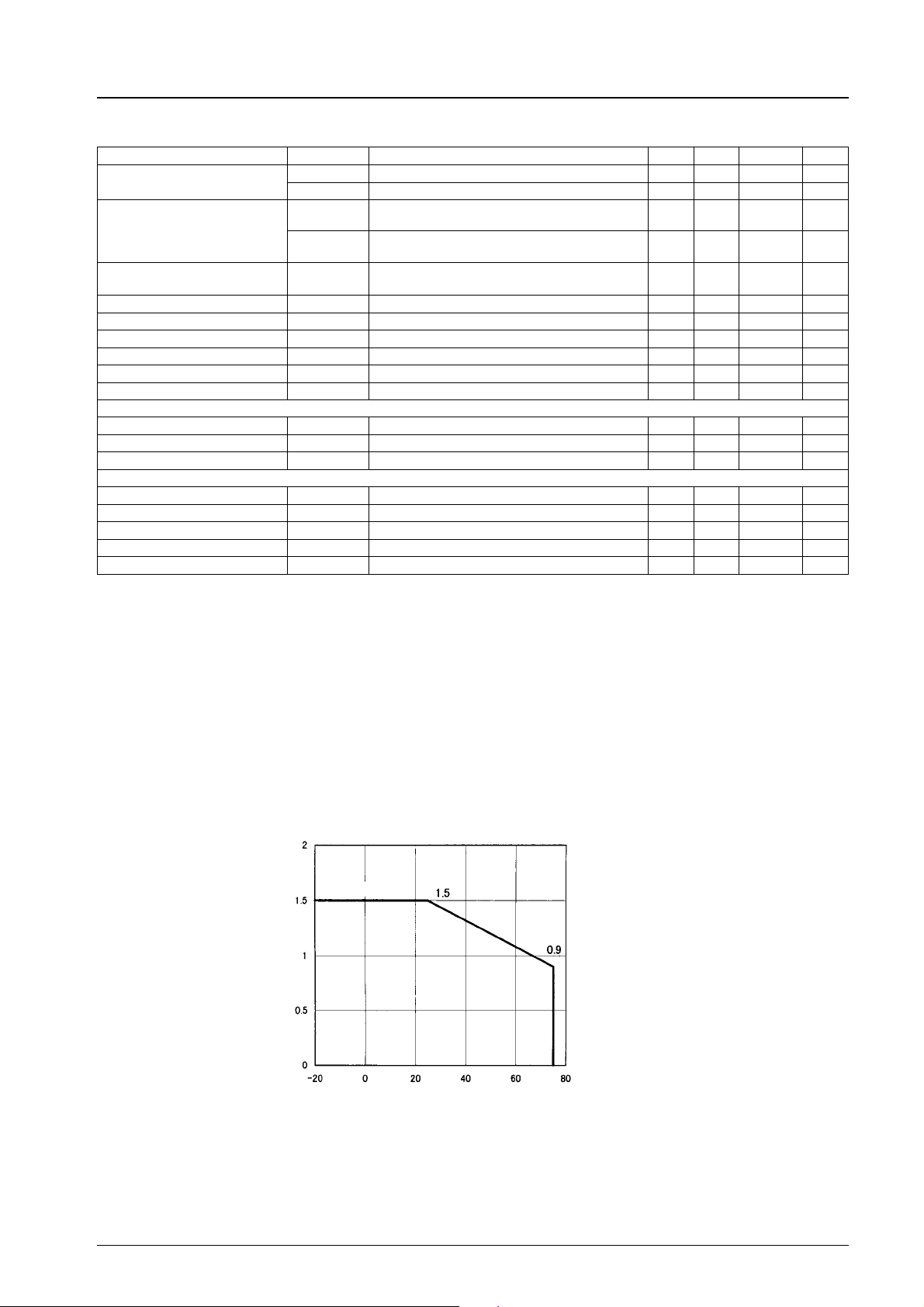
Electrical Characteristics at Ta = 25°C, VCC= 8.0 V, V
Parameter Symbol
No-load current drain
V
Output offset voltage
V
Buffer amplifier input voltage
range
Input voltage range V
Output source voltage V
Output sink voltage V
I
1 When all amplifier outputs are on (Mute high) 20 40 mA
CC
I
2 When all amplifier outputs are off (Mute low) 15 35 mA
CC
OF
OF
V
BIN
IN
O
O
Amplifier 1 to 2 (V
1
Amplifier 3 to 4 (V
Amplifier 5 to 6 (V
2
Amplifier 7 to 8 (V
1 Note 1, when RL= 8.0 Ω 5.0 5.6 V
2 Note 2, when RL= 8.0 Ω 1.8 2.4 V
Conditions
1toVO2),
O
3toVO4)
O
5toVO6),
O
7toVO8)
O
REF
=4V
min typ max Unit
–50 50 mV
–50 50 mV
1.5
1.0
VCC−1.5
VCC−1.5
Closed-circuit voltage gain VG Between bridge amplifiers 9 dB
Slew rate SR 0.15 V/µs
Mute on voltage V
Mute
Note 3 1.2 V
[Power Supply] (with 2SK632K connected externally)
Output voltage V
Line regulation ∆V
Load regulation ∆V
1I
OUT
OLN
OLD
= 200 mA 4.75 5.0 5.25 V
O
1 5.6 % VIN1 % 12 V 20 100 mV
15mA%IO%200 mA 50 150 mV
[Reset]
High reset output voltage V
Low reset output voltage V
Reset threshold voltage V
ORH
ORL
RT
I
= 200 µA, Cd pin open 4.73 4.98 5.23 V
ORH
I
= 2 mA, Cd is shorted to GND 100 200 mV
SRL
Note 4 4.3 V
Reset hysteresis voltage Vhys Note 5 40 100 200 mV
Reset output delay time td Cd = 0.1 µF 10 ms
V
V
Notes:
1. Source voltage to ground when an 8 Ω load is connected between bridge amplifier outputs.
2. Sink voltage to ground when an 8 Ω load is connected between bridge amplifier outputs.
3. When the mute signal is high, all amplifier outputs turn on, and when low, all amplifier outputs turn off. When the mute
signal is low, amplifier output is undefined.
4. 5 V supply voltage when the reset output goes low.
5. Potential difference from the 5 V supply voltage when the reset output goes low and when it goes high.
Pd max – Ta
Independent IC
Allowable power dissipation, Pd max – W
Ambient temperature, Ta – °C
No. 5591- 2/7
Page 3

LA6541D
Pin Functions
Pin No. Pin Name Description (Function)
1V
CC
2 Mute ON/OFF control for all BTL AMP outputs
3V
1 BTL AMP 1 input
IN
4 VG1 BTL AMP 1 input (for gain control)
5V
6V
1 BTL AMP 1 output (non-inverting side)
O
2 BTL AMP 1 output (inverting side)
O
7 GND GND (minimum electric potential)
8 GND GND (minimum electric potential)
9 GND GND (minimum electric potential)
10 V
11 V
3 BTL AMP 2 output (inverting side)
O
4 BTL AMP 2 output (non-inverting side)
O
12 VG2 BTL AMP 2 input (for gain control)
13 V
2 BTL AMP 2 input
IN
14 REG OUT Connection for collector of external transistor (PNP); 5 V supply output
15 REG IN Connection for base of external transistor (PNP)
16 RES
17 C
18 V
D
3 BTL AMP 3 input
IN
19 VG3 BTL AMP 3 input (for gain control)
20 V
21 V
5 BTL AMP 3 output (non-inverting side)
O
6 BTL AMP 3 output (inverting side)
O
22 GND GND (minimum electric potential)
23 GND GND (minimum electric potential)
24 GND GND (minimum electric potential)
25 V
26 V
7 BTL AMP 4 output (inverting side)
O
8 BTL AMP 4 output (non-inverting side)
O
27 VG4 BTL AMP 4 input (for gain control)
28 V
29 V
30 V
4 BTL AMP 4 input
IN
REF
CC
Power supply (shorted with pin 30)
Reset output
Reset output delay time setting (with capacitor)
Reference voltage input for level shift circuit
Power supply (shorted with pin 1)
No. 5591- 3/7
Page 4
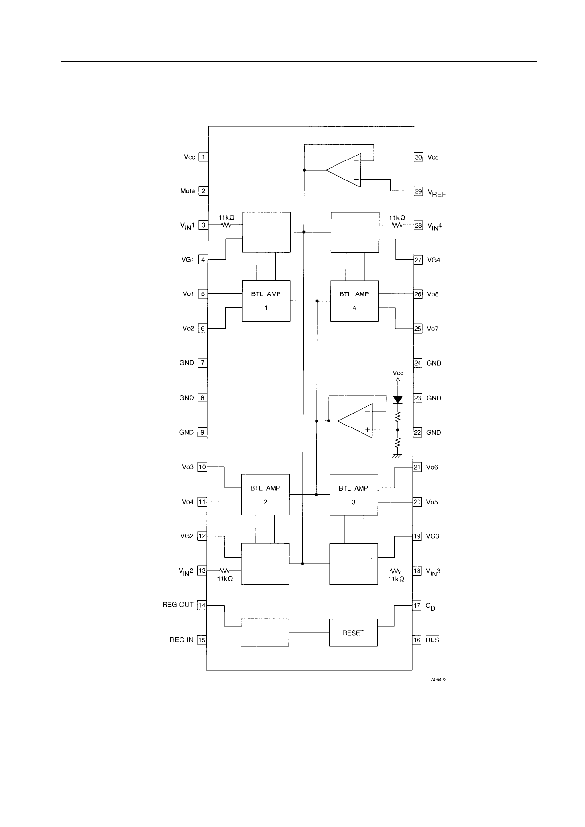
Pin Assignment (Block Diagram)
LA6541D
Level shift
1
Level shift
4
Level shift
2
Regulator
Level shift
3
Top view
No. 5591- 4/7
Page 5
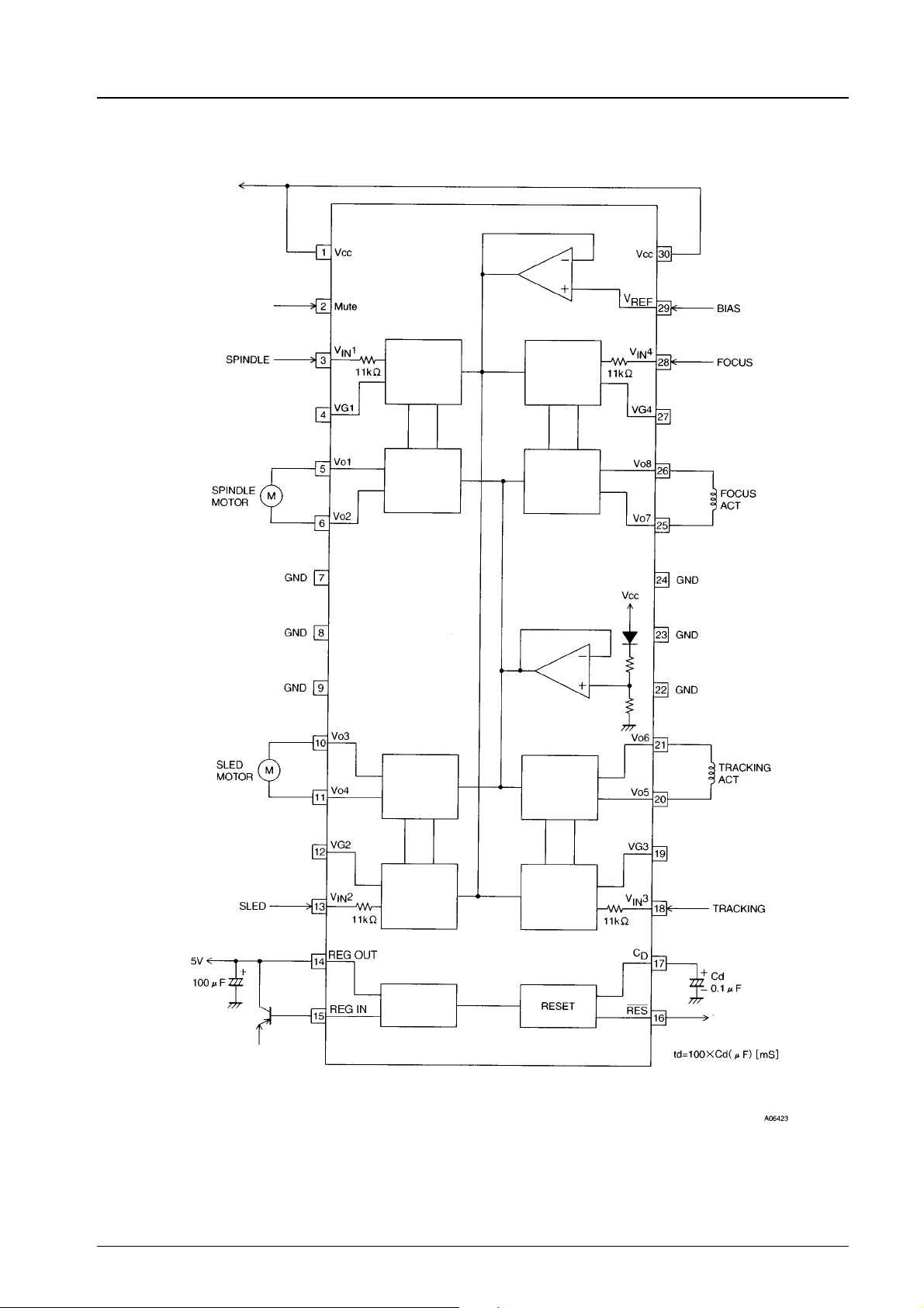
Sample Application Circuit
To V
CC
Microcontroller
LA6541D
Level
shift
BTL
driver
BTL
driver
Level
shift
BTL
driver
BTL
driver
Level
shift
Regulator
V
CC
Level
shift
Microcontroller
(connected to pins 1 and 30)
Note: Use a delay capacitor (Cd) whose capacitance does not change much according to the temperature.
No. 5591- 5/7
Page 6
LA6541D
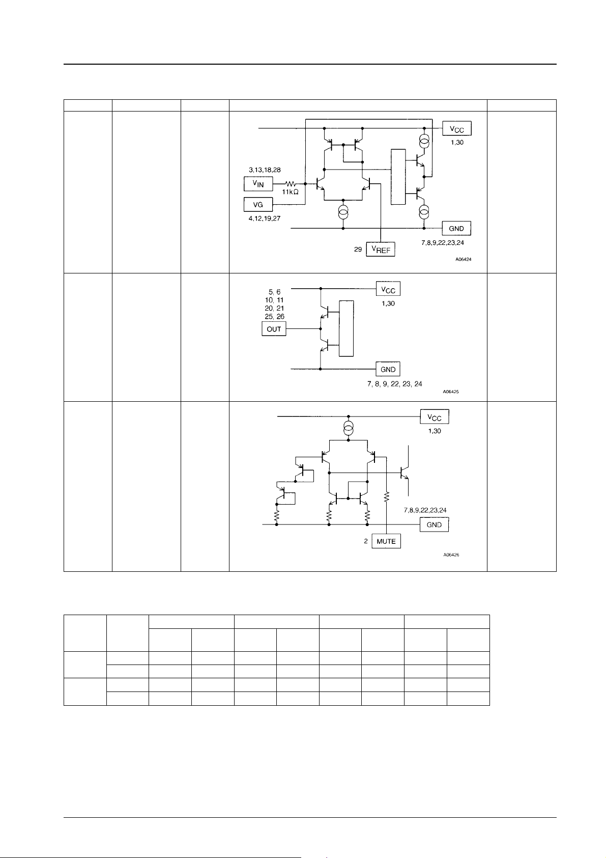
Pin Functions
Pin Name Pin No. Equivalent Circuit Description
Input V
IN
V
IN
V
IN
V
IN
VG1
VG2
VG3
VG4
1
2
3
4
3
13
18
28
4
12
19
27
Input pins
Output V
Mute Mute 2
O
V
O
V
O
V
O
1, VO2
3, VO4
5, VO6
7, VO8
5, 6
10, 11
20, 21
25, 26
Output pins
Output ON/OFF
Truth Table
Input MUTE
H
L
CH1 CH2 CH3 CH4
V
1
O
(Amp1)
HHL LHHL LH
L ————————
HLHHLLHHL
L ————————
VO2
(Amp2)
VO3
(Amp3)
VO4
(Amp4)
VO5
(Amp5)
VO6
(Amp6)
VO7
(Amp7)
VO8
(Amp8)
* The ‘‘—’’ symbol means ‘‘undefined.’’
No. 5591- 6/7
Page 7
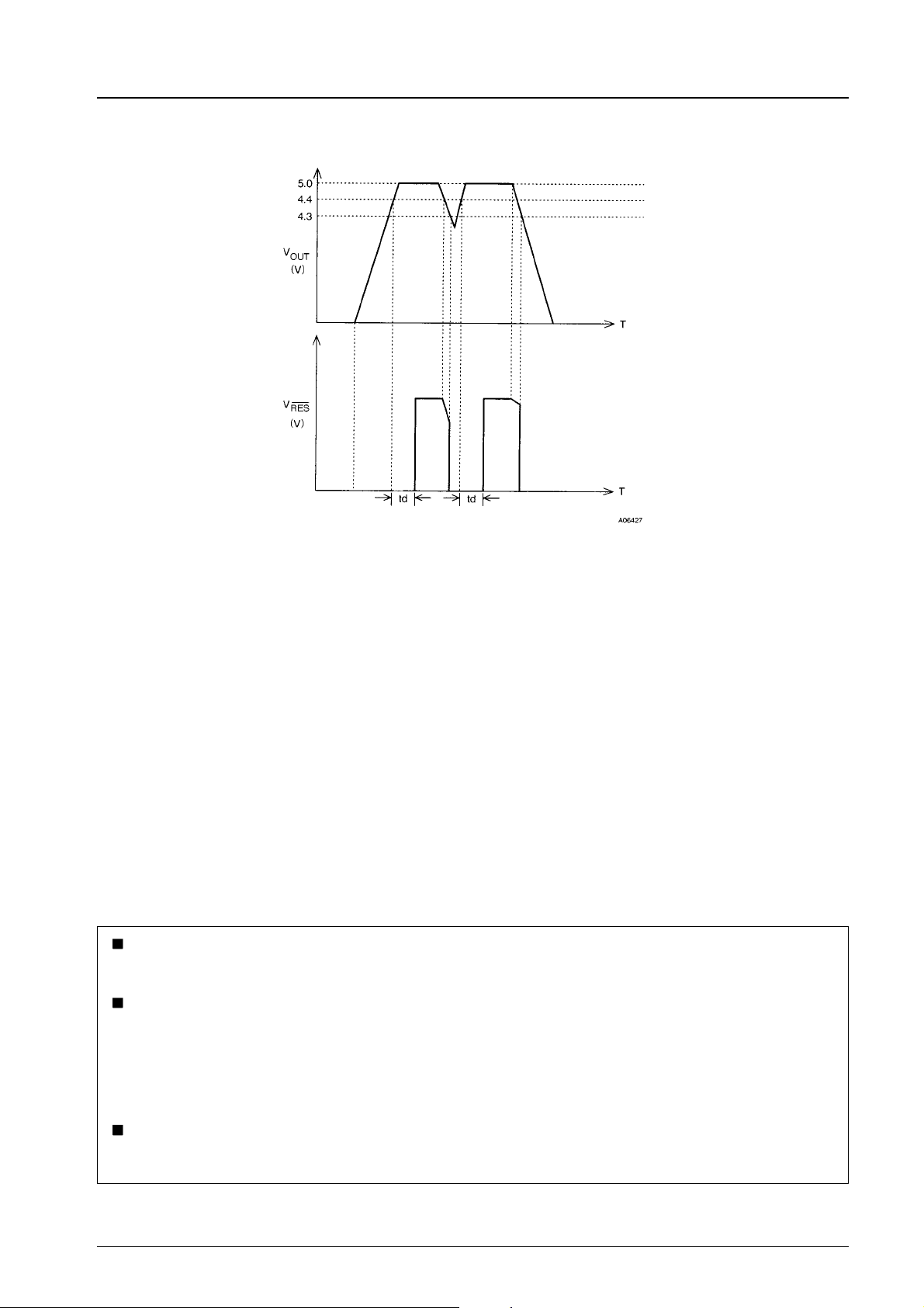
Reset Operation
LA6541D
No products described or contained herein are intended for use in surgical implants, life-support systems,
aerospace equipment, nuclear power control systems, vehicles, disaster/crime-prevention equipment and the like,
the failure of which may directly or indirectly cause injury, death or property loss.
Anyone purchasing any products described or contained herein for an above-mentioned use shall:
1 Accept fullresponsibilityand indemnify and defend SANYOELECTRIC CO., LTD.,itsaffiliates, subsidiaries and
distributors and all their officers and employees, jointly and severally, against any and all claims and litigation
and all damages, cost and expenses associated with such use:
2 Not impose any responsibility for any fault or negligence which may be cited in any such claim or litigation on
SANYO ELECTRIC CO., LTD., its affiliates, subsidiaries and distributors or any of their officers and employees
jointly or severally.
Information (including circuit diagrams and circuit parameters) herein is for example only; it is not guaranteed for
volume production. SANYO believes information herein is accurate and reliable, but no guarantees are made or
implied regarding its use or any infringements of intellectual property rights or other rights of third parties.
This catalog provides information as of December, 1996. Specifications and information herein are subject to change without notice.
No. 5591- 7/7
 Loading...