

Page 1
Ordering number: EN2704B
Monolithic Linear IC
LA6324N, 6324NM
High-Performance
Quad Operational Amplifier
Overview
The LA6324 consists of four independent, high-performance,
internally phase compensated operational amplifiers that are
designed to operate from a single power supply over a wide
range of voltages. These four operational amplifiers are
packaged in a single package. As in case of conventional
general-purpose operational amplifiers, operation from dual
power supplies is also possible and the power dissipation is
low. It can be applied to various uses in commercial and
industrial equipment including all types of transducer
amplifiers and DC amplifiers.
Features
.
No phase compensation required
.
Wide operating voltage range:
3.0 V to 30.0 V (single supply)
±1.5Vto±15.0 V (dual supplies)
.
Highly resistant to dielectric breakdown
.
Input voltage range includes the neighborhood of GND level
and output voltage range V
.
Small current dissipation:
I
= 0.6 mA typ/VCC=+5V,RL=∞
CC
is from 0 to VCC− 1.5 V.
OUT
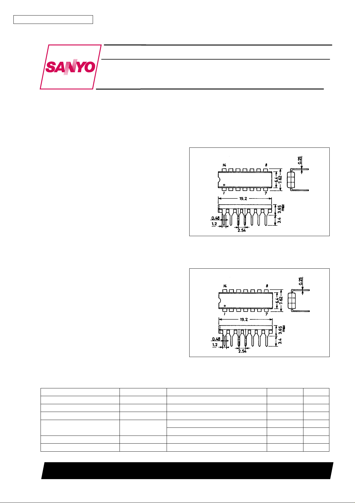
Package Dimensions
unit : mm
3003A-DIP14
[LA6324N]
SANYO : DIP14
unit : mm
3034A-MFP14
[LA6324NM]
SANYO : MFP14
Specifications
Maximum Ratings at Ta = 25°C
Parameter Symbol Conditions Ratings Unit
Maximum supply voltage V
Differential input voltage V
Maximum input voltage V
Allowable power dissipation Pd max LA6324N 720 mW
Operating temperature Topr –30 to +85 °C
Storage temperature Tstg –55 to +125 °C
max 32 V
CC
ID
max –0.3 to +32 V
IN
LA6324NM 330 mW
32 V
SANYO Electric Co.,Ltd. Semiconductor Bussiness Headquarters
TOKYO OFFICE Tokyo Bldg., 1-10, 1 Chome, Ueno, Taito-ku, TOKYO, 110 JAPAN
63096HA(II)/4138TA(KOTO) No.2704-1/5
Page 2
LA6324N, 6324NM
Operating Characteristics at Ta = 25°C, VCC=+5V
Parameter Symbol Conditions Test circuit min typ max Unit
Input offset voltage V
Input offset current I
Input bias current I
Common-mode input voltage
range
IO
IIN(+)/IIN(–) 2 ±5 ±50 nA
IO
IIN(+)/IIN(–) 3 45 250 nA
B
V
ICM
Common-mode rejection ratio CMR 4 65 80 dB
Voltage gain VG V
Output voltage range V
OUT
=15V,RL^2kΩ 5 25 100 V/mV
CC
Supply voltage rejection ratio SVR 6 65 100 dB
Channel separation CS f=1kto20kHz 7 120 dB
I
Current drain
Output current (Source) I
Output current (Sink) I
CC
I
CC
source V
O
sink V
O
VCC=30V 8 1.5 3 mA
+
IN
+
IN
=1V,V
=0V,V
–
=0V 9 20 40 mA
IN
–
= 1 V 10 10 20 mA
IN
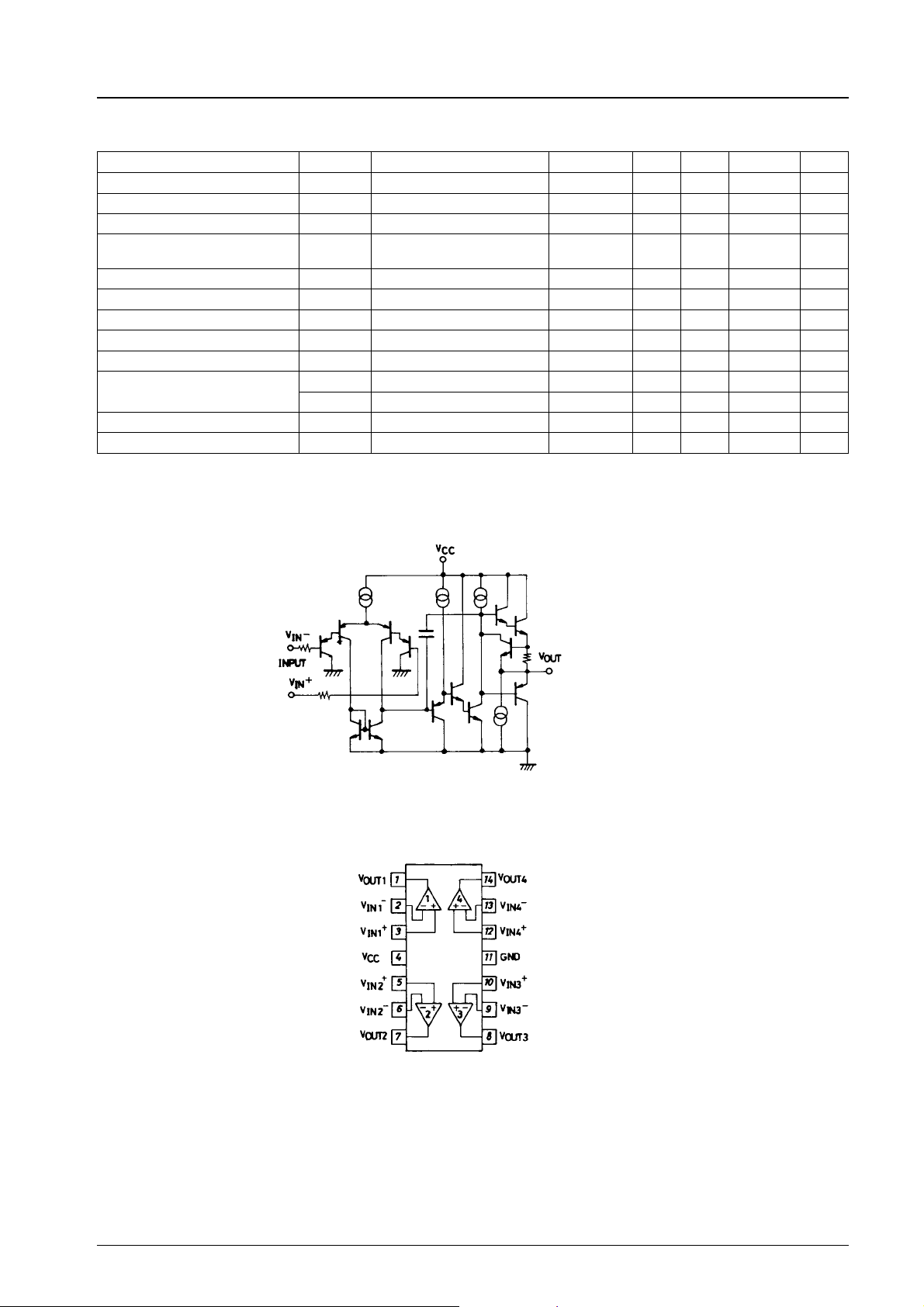
Equivalent Circuit
(1 unit)
1 ±2 ±7mV
40 V
0V
– 1.5 V
CC
– 1.5 V
CC
8 0.6 2 mA
Pin Assignment
(LA6324N, 6324NM)
Top view
No.2704-2/5
Page 3
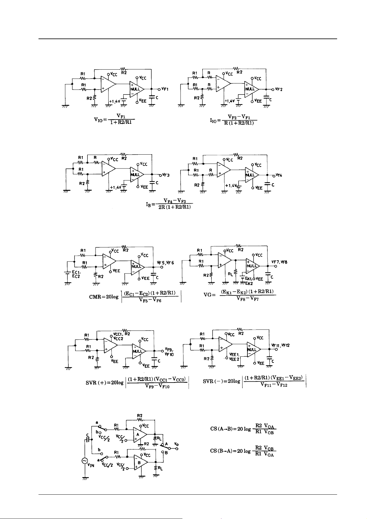
Test Circuit
1. Input offset voltage V
LA6324N, 6324NM
IO
2. Input offset current I
IO
3. Input bias current I
B
4. Common-mode rejection ratio CMR
Common-mode input voltage range V
5. Voltage gain VG
ICM
6. Supply voltage rejection ratio SVR
7. Channel separation CS
SW: a
SW: b
These apply also to other channels.
No.2704-3/5
Page 4
LA6324N, 6324NM
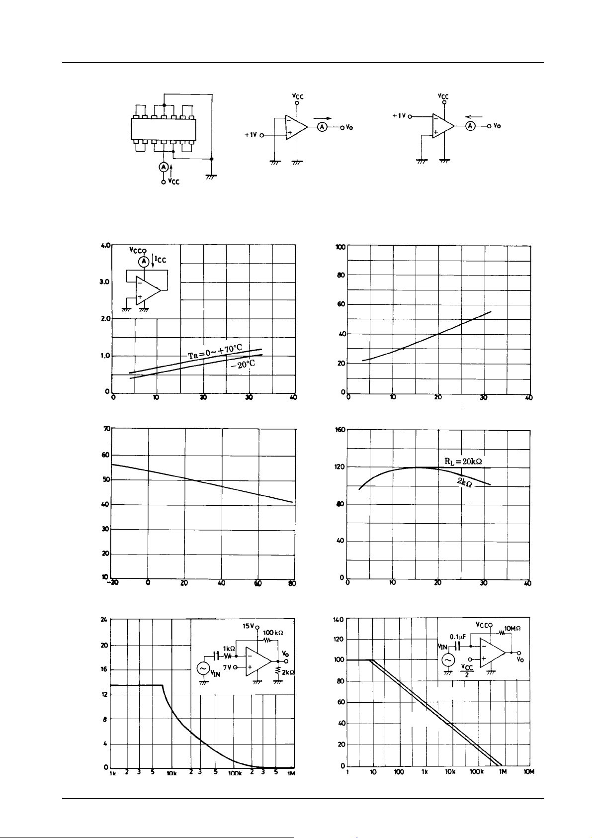
8. Current drain I
–mA
CC
Current drain, I
CC
ICC–V
9. Output current IOsource 10. Output current IOsink
CC
–nA
B
IB–V
Input bias current, I
CC
(source) – mA
O
Output current, I
– Vp-p
OUT
Supply voltage, VCC–V
IO(source) – Ta
Ambient temperature, Ta – °C
VO–f
Supply voltage, VCC–V
VG–V
CC
Voltage gain, VG – dB
Supply voltage, VCC–V
VG–f
VCC=30V
10 to 15 V
Voltage gain, VG – dB
Output voltage amplitude, V
Frequency,f–Hz
Frequency,f–Hz
No.2704-4/5
Page 5
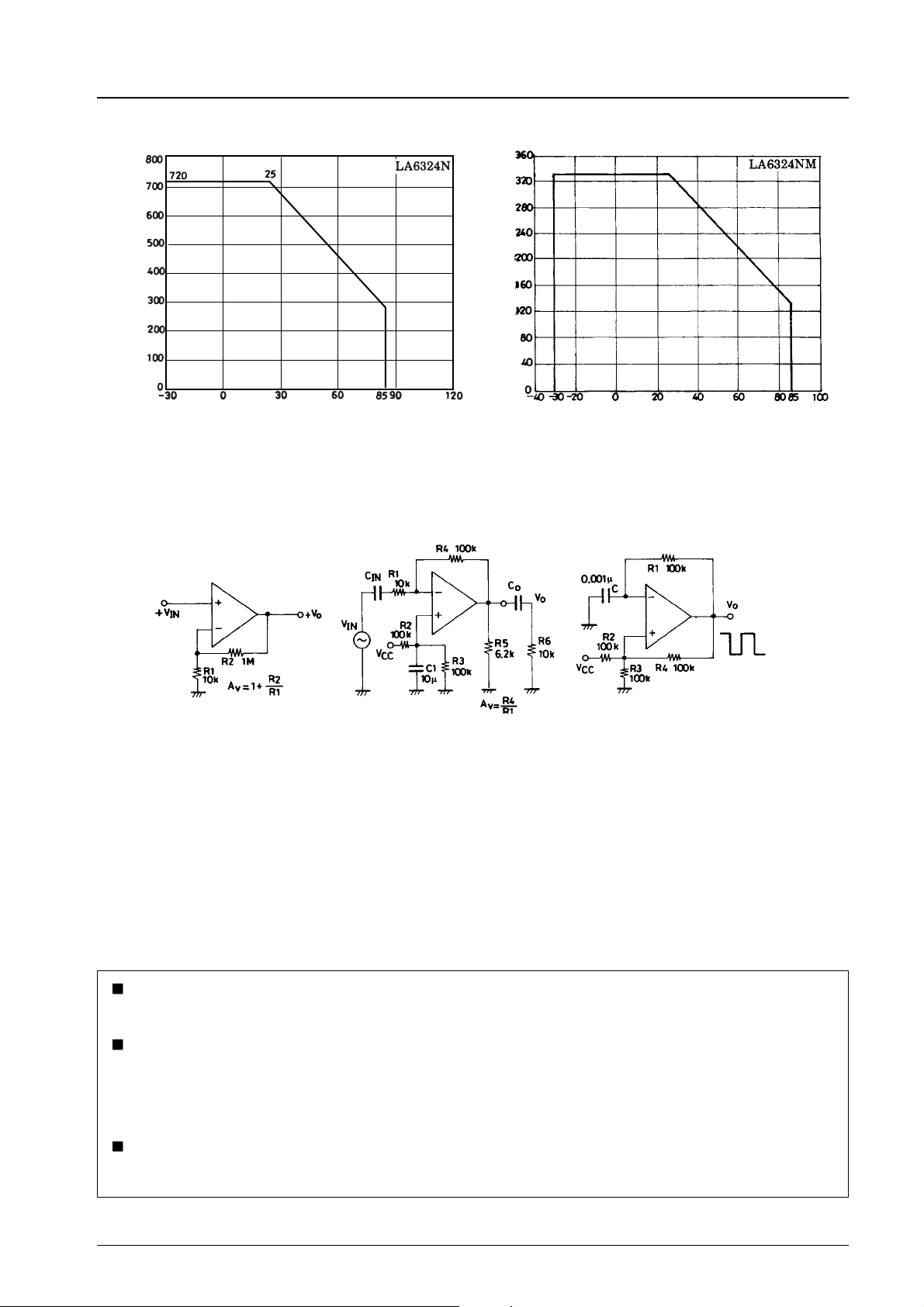
LA6324N, 6324NM
Pd max – Ta
Allowable power dissipation, Pd max – mW
Ambient temperature, Ta – °C
Sample Application Circuits
Noninverting DC amplifier Inverting AC amplifierRectangular wave oscillator
Allowable power dissipation, Pd max – mW
Pd max – Ta
Ambient temperature, Ta – °C
Unit (resistance: Ω, capacitance: F)
No products described or contained herein are intended for use in surgical implants, life-support systems, aerospace equipment,
nuclear power control systems, vehicles, disaster/crime-prevention equipment and the like, the failure of which may directly or
indirectly cause injury, death or property loss.
Anyone purchasing any products described or contained herein for an above-mentioned use shall:
1 Accept full responsibility and indemnify and defend SANYO ELECTRIC CO., LTD., its affiliates, subsidiaries and distributors
and all their officers and employees, jointly and severally, against any and all claims and litigation and all damages, cost and
expenses associated with such use:
2 Not impose any responsibility for any fault or negligence which may be cited in any such claim or litigation on SANYO
ELECTRIC CO., LTD., its affiliates, subsidiaries and distributors or any of their officers and employees jointly or severally.
Information (including circuit diagrams and circuit parameters) herein is for example only; it is not guaranteed for volume
production. SANYO believes information hereinisaccurate and reliable, but no guarantees are made or implied regarding its use
or any infringements of intellectual property rights or other rights of third parties.
This catalog provides information as of June, 1996. Specifications and information herein are subject to change without notice.
No.2704-5/5
 Loading...