

Page 1
Parameter Symbol Conditions Ratings Unit
Maximum supply voltage
V
CC
1 max 14
V
V
CC
2 max VCC1 ≥ VCC2V
CC
1
Allowable power dissipation Pd max No heat sink 1.7 W
Operating temperature Topr –20 to +80 °C
Storage temperature Tstg –40 to +150 °C
Ordering number : EN5669
53197HA(OT) No. 5669-1/4
Overview
The LA5613 is an IC that includes an independently
on/off switchable 5-V/0.7-A low-saturation regulator, an
11.3-V/0.3-A ripple filter, and a control amplifier on chip.
It is optimal for use in VCR and similar products.
Functions and Features
• 5-V/0.7-A low-saturation regulator
(Includes an on/off function.)
• 11.3-V/0.3-A ripple filter (Includes an on/off function.)
• Switching regulator control amplifier
• Includes input overvoltage and thermal protection
circuits on chip.
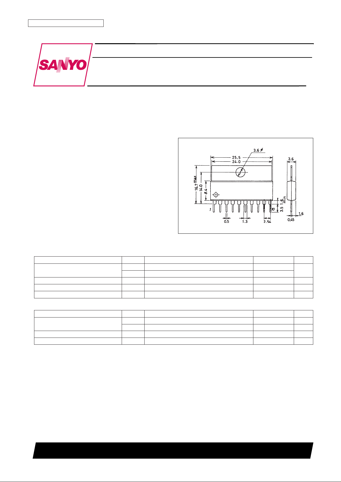
Package Dimensions
unit: mm
3046B-SIP10F
SANYO: SIP10H
[LA5613]
LA5613
SANYO Electric Co.,Ltd. Semiconductor Bussiness Headquarters
TOKYO OFFICE Tokyo Bldg., 1-10, 1 Chome, Ueno, Taito-ku, TOKYO, 110 JAPAN
Monolithic Linear IC
Specifications
Maximum Ratings at Ta = 25°C
Parameter Symbol Conditions Ratings Unit
Input voltage
V
CC
1 12.3 ± 0.4 V
V
CC
2 6 ± 0.5 V
Output current 1 I
O
1 0 to 0.3 A
Output current 2 I
O
2 0 to 0.7 A
Operating Conditions at Ta = 25°C
VCR Regulator and Control Amplifier
Page 2
Parameter Symbol Conditions
Ratings
Unit
min typ max
[No Load] V
STB
= high, VCC1 = 12.3 V, VCC2 = 6 V, IO1 and IO2 = 0 A
Quiescent current
I
IN
1 – 20 30 mA
I
IN
2 – 0.2 0.3 mA
[Output 1] V
STB
= high, VCC1 = 12.3 V, VCC2 = 6 V, IO1 = 0.3 A
Output voltage 1 V
O
1 10.9 11.3 – V
Dropout voltage V
DROP
1 – 1.0 1.4 V
Peak output current I
OP
1 0.3 – – A
Output low-level voltage V
O1 OFF
– – 0.2 V
[Output 2] V
STB
= high, VCC1 = 12.3 V, VCC2 = 6 V, IO2 = 0.7 A
Output voltage 2 V
O
2 4.9 5.1 5.3 V
Dropout voltage V
DROP
2 – 0.3 0.5 V
Line regulation ∆V
OLN
2 6 V ≤ VCC2 ≤ 7 V – – 20 mV
Load regulation ∆V
OLD
2 0.1 A ≤ IO2 ≤ 0.7 A – – 300 mV
Peak output current I
OP
2 0.7 – – A
Output short-circuit current I
OSC
2 – – 0.75 A
Ripple rejection Rrej2 f = 120 Hz, 6 V ≤ V
CC
2 ≤ 7 V – 50 – dB
Output low-level voltage V
O
2 OFF – – 0.2 V
[Input Overvoltage Protection]
Detection voltage V
HVTH
7.6 8.0 8.4 V
[Output 1 and Output 2 On/Off Control] V
CC
1 = 12.3 V, VCC2 = 6 V
Output off control voltage V
STB
L VO1 and VO2: off – – 1.0 V
Output on control voltage V
STB
H VO1 and VO2: on 3.0 – VCC1
[Control Amplifier] V
CC
1 = 12.3 V, VCC2 = 6 V
Control output current (sink) I
CONT
VCC1 = 12.8 V 10 – – mA
Resistance ratio KR KR = R1/R2, V
REF
= 1.28 V typ – 8.61 –
Output inverted input voltage V
CC
1 - ERR IO1 = 0.3 A, IO2 = 0.7 A 11.9 12.3 12.7 V
No. 5669-2/4
LA5613
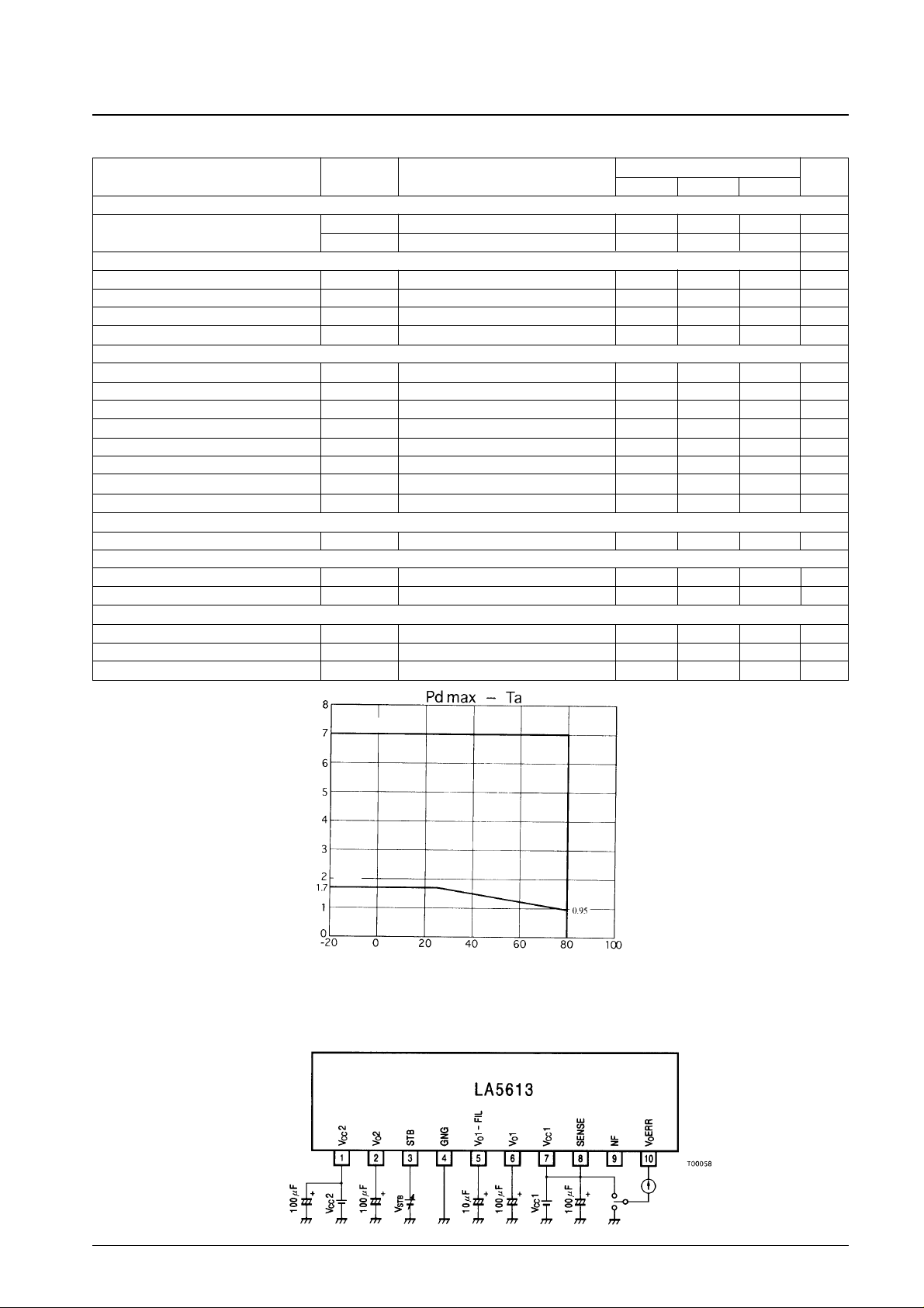
Electrical Characteristics at Ta = 25°C in the specified Test Circuit
Test Circuit
Ambient temperature, Ta – °C
Allowable power dissipation, Pd max – W
Page 3
No. 5669-3/4
LA5613
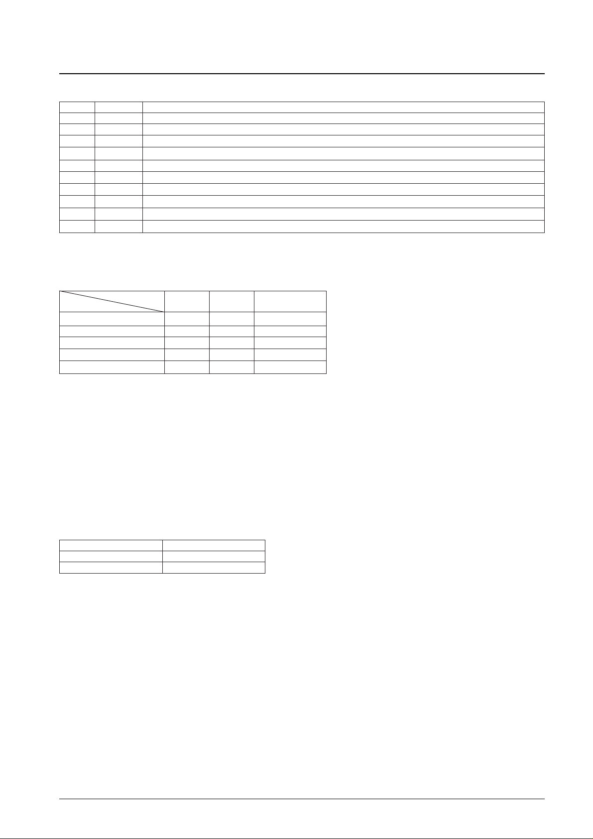
Pin Functions
Function Table (❍: built-in, ×: not built-in)
Usage Notes
Pin No. Symbol Function
1 V
CC
2 Low-voltage input
2 V
O
2 5.1-V/0.7-A regulator output, with on/off, current limiter thermal shutdown.
3 STB V
O
1 and VO2 on/off control. Active high.
4 GND Substrate of the LA5613 (minimum potential)
5 V
O
1-FIL VO1 ripple filter capacitor connection
6 V
O
1 Ripple filter 0.3-A output, with on/off, current limiter thermal shutdown.
7 V
CC
1 High-voltage input
8 SENSE V
CC
1 voltage detection
9 NF Phase compensation and V
CC
1 adjustment. Connect resistors between this pin and SENSE or ground.
10 V
O
ERR Switching register control amplifier drive output
Notes: 1. CL: Current limiter
2. TSD: Thermal shutdown
Circuit block
V
O
1 VO2 Control amplifier
Function
Input line V
CC
1 VCC2 VCC1
Output current protection ❍ ❍ ×
Thermal shutdown protection ❍ ❍ ×
On/off control ❍ ❍ ×
Overvoltage protection ❍ ❍ ❍
• The relationship VCC1 ≥ VCC2 must hold at all times when power is applied.
• Power should be applied to VCC1 and VCC2 simultaneously. Do not use this IC with only one or the other voltage
applied.
• This IC will be destroyed if the VO1 output load is shorted. Do not short the outputs of this IC.
Logic Table
Conditions: When VCC1 ≥ VCC2
(However, the conditions 11.9 V ≤ VCC1 ≤ 12.7 V and 5.5 V ≤ VCC2 ≤ 6.5 V must also apply.)
STB VO1, VO2
L or open L
H H
Notes: 1. "H" for STB denotes high level; "L" denotes low level.
2. "H" for V
O
denotes output ON voltage; "L" denotes output OFF voltage.
Page 4
No. 5669-4/4
LA5613
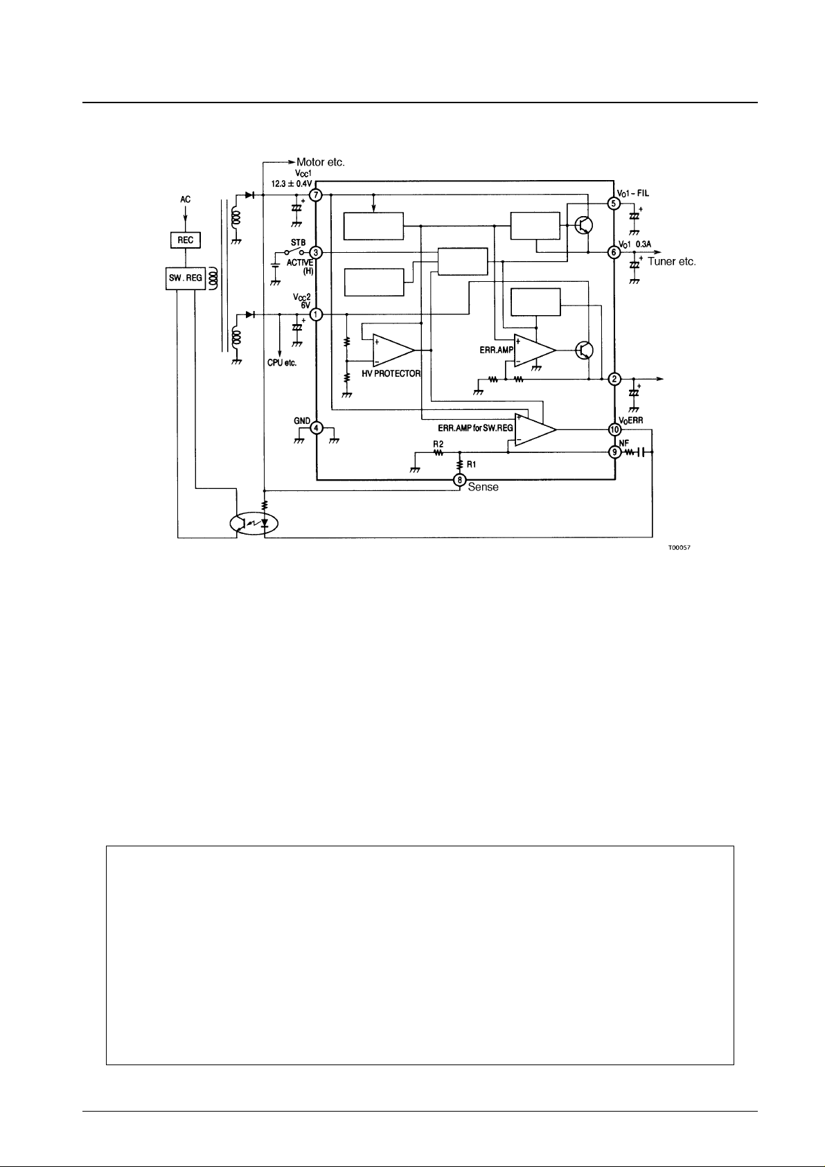
Equivalent Circuit Block Diagram and Sample Application Circuit
This catalog provides information as of May, 1997. Specifications and information herein are subject to change
without notice.
■ No products described or contained herein are intended for use in surgical implants, life-support systems, aerospace
equipment, nuclear power control systems, vehicles, disaster/crime-prevention equipment and the like, the failure of
which may directly or indirectly cause injury, death or property loss.
■ Anyone purchasing any products described or contained herein for an above-mentioned use shall:
➀ Accept full responsibility and indemnify and defend SANYO ELECTRIC CO., LTD., its affiliates, subsidiaries and
distributors and all their officers and employees, jointly and severally, against any and all claims and litigation and all
damages, cost and expenses associated with such use:
➁ Not impose any responsibility for any fault or negligence which may be cited in any such claim or litigation on
SANYO ELECTRIC CO., LTD., its affiliates, subsidiaries and distributors or any of their officers and employees
jointly or severally.
■ Information (including circuit diagrams and circuit parameters) herein is for example only; it is not guaranteed for
volume production. SANYO believes information herein is accurate and reliable, but no guarantees are made or implied
regarding its use or any infringements of intellectual property rights or other rights of third parties.
Reference
regulator
Thermal
shutdown
protector
On/off
control
Current
limiter
Current
limiter
VO2 5.1 V/0.7 A
AUDIO AMP
etc.
Photocoupler
 Loading...