

Page 1
Overview
The LA4906 is a BTL two-channel power amplifier for
use in car audio systems. It uses a signal-following
switching technique in the power supply for the amplifier
output stage and a newly-developed nonlinear amplifier
that features nonlinear characteristics in the signal system.
These features hold increases in the number of external
components to a minimum, and reduce power dissipation
(and thus heat generation) in the practical operating region
to about 1/2 that of earlier class B amplifier ICs. This can
contribute significantly to miniaturization and weight
reduction in the heat sink and to reduction of the heat
generated within the end product case.
Features
• Power dissipation reduced by 50% (for music at average
power levels, as compared to earlier Sanyo products)
• The number of required signal-following switching
circuits has been reduced to just one circuit for two
channels, reducing the number of external components.
• The output is a pure analog signal; no switching noise
whatsoever appears on the output lines.
• Uses a single-voltage power supply from 8 to 18 V.
• Provides a full range of built-in protection circuits,
including shorting of output pin to VCC, shorting of
output pin to ground, overvoltage, and thermal
shutdown protection.
• Built-in standby switch
• Clipping detection function
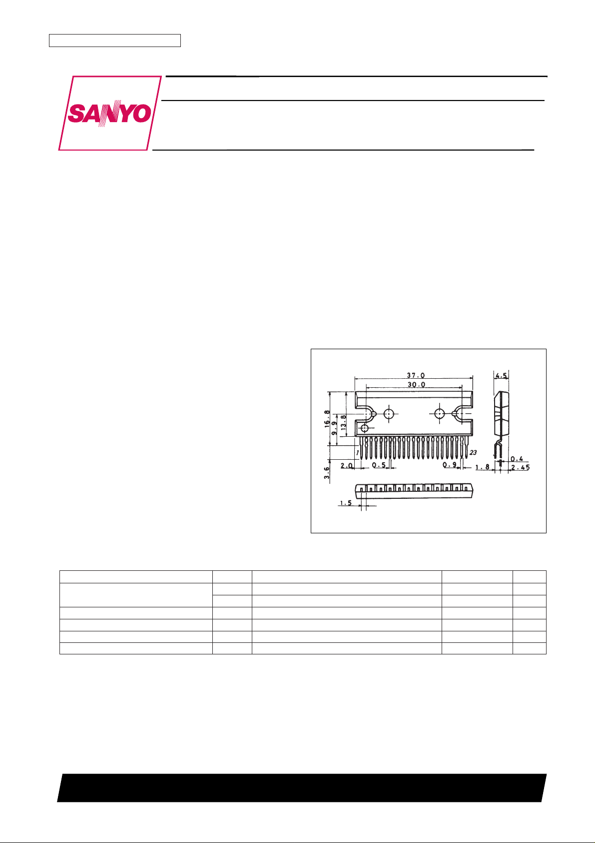
Package Dimensions
unit: mm
3160-SIP23HZ
Monolithic Linear IC
Ordering number : EN *5714
73097HA(OT) No. 5714-1/10
Preliminary
SANYO: SIP23HZ
[LA4906]
SANYO Electric Co.,Ltd. Semiconductor Bussiness Headquarters
TOKYO OFFICE Tokyo Bldg., 1-10, 1 Chome, Ueno, Taito-ku, TOKYO, 110 JAPAN
17-W, 2-Channel BTL AF High-Efficiency
Power Amplifier for Car Audio Systems
LA4906
Parameter Symbol Conditions Ratings Unit
Maximum supply voltage
V
CC
max1 With no signal, t = 1 minute 18 V
V
CC
max2 16 V
Maximum output current I
O
Peak Per channel 4.5 A
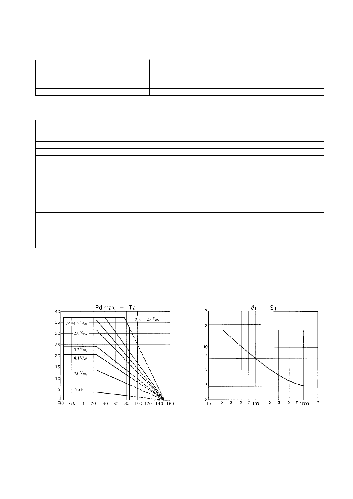
Allowable power dissipation Pd max With an arbitrarily large heat sink 37.5 W
Operating temperature Topr –35 to +85 °C
Storage temperature Tstg –40 to +150 °C
Specifications
Absolute Maximum Ratings at Ta = 25°C
Notes: 1. Set VCCand RLto be in the range where Pd max does not exceed 37.5 W.
2. The overvoltage protection circuit operates at V
CC
= 26 V or higher.
Page 2
No. 5714-2/10
LA4906
Parameter Symbol Conditions
Ratings
Unit
min typ max
Quiescent current drain I
CC
0 RL= ∞, VIN= 0 80 110 150 mA
Standby current Ist 0 10 µA
Voltage gain VG V
O
= 0 dBm 28 30 32 dB
Total harmonic distortion THD P
O
= 1 W, LPF = 30 kHz 0.07 0.2 %
Output power
P
O
1 THD = 10 %, RL = 4 Ω 14 17 W
P
O
2 THD = 10 %, RL = 2 Ω 25 W
Output noise voltage V
NO
Rg = 0, BPF = 20 Hz to 20 kHz 0.10 0.3 mVrms
Ripple rejection ratio SVRR
Rg = 0, V
CCR
= 0 dBm,
60 75 dB
BPF = 20 Hz to 20 kHz
Channel separation CH sep
Rg = 10 kΩ, V
O
= 0 dBm,
45 60 dB
BPF = 20 Hz to 20 kHz
Input resistance Ri 21 30 39 kΩ
Output offset voltage VN offset Rg = 0 –200 +200 mV
Standby on voltage V
STH
AMP = on, applied through a 10 kΩ resistor 3 V
CC
V
Clipping detect off current I
DOFF
THD = 1 % 1 10 µA
Clipping detect on current I
DON
THD = 10 % 100 150 200 µA
Operating Characteristics
at Ta = 25°C, VCC= 13.2 V, RL= 4 Ω, f = 1 kHz, RG = 600 Ω, in the recommended circuit
Parameter Symbol Conditions Ratings Unit
Recommended supply voltage V
CC
13.2 V
Allowable operating voltage range V
CC
op 8 to 16 V
Recommended load resistance R
L
4 Ω
Recommended load resistance range R
L
op 2 to 4 Ω
Operating Conditions at Ta = 25°C
Note: Set VCCand RLto be in the range where Pd max does not exceed 37.5 W.
Allowable power dissipation, Pd max – W
Heat sink thermal resistance,
θf – °C/W
Heat sink area, Sf – cm
2
Ambient temperature, Ta – °C
With an arbitrarily large heat sink
Al heat sink, t = 1.5 mm
Tightening torque: 39 N·cm
With silicone grease applied.
Page 3
No. 5714-3/10
LA4906
Technologies for Increased Efficiency Used in the LA4906
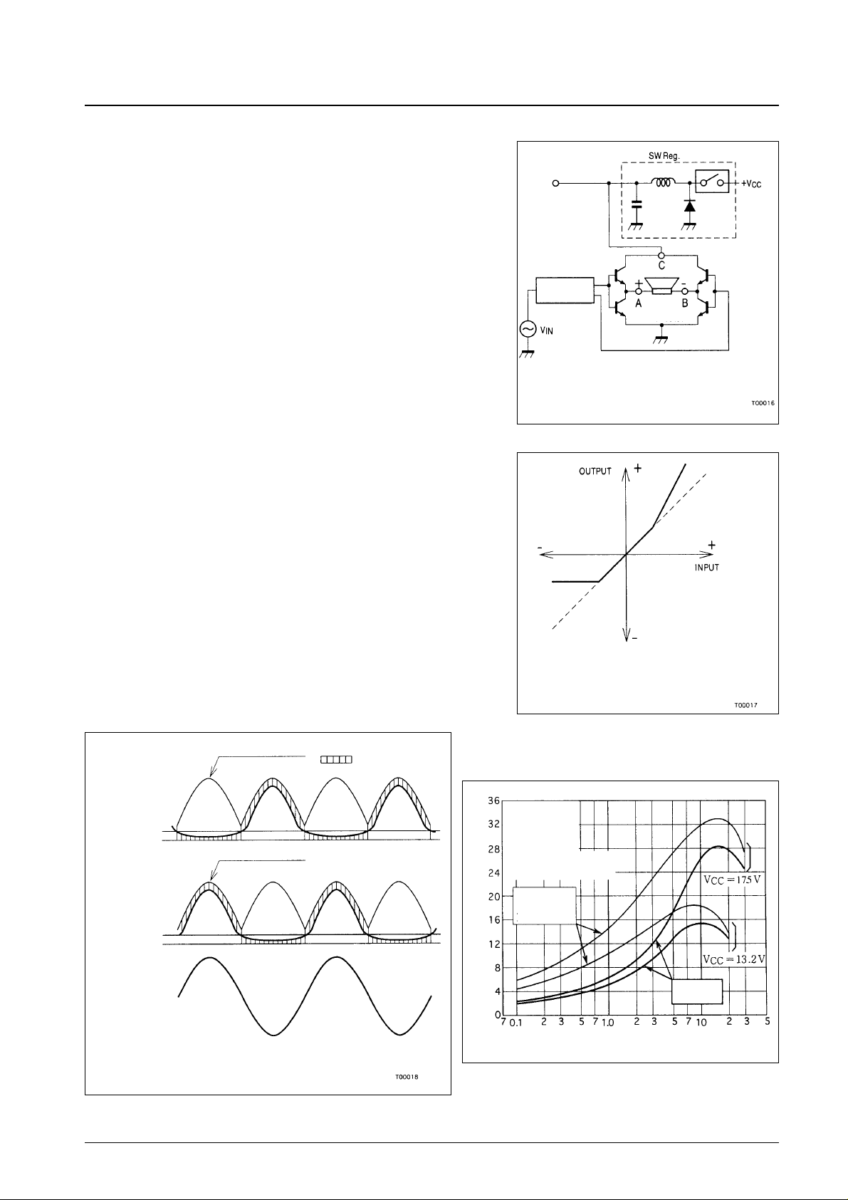
• Nonlinear amplifier
The LA4906 adopts a nonlinear amplifier, which has the nonlinear
characteristics shown in Figure 2, in the signal system. The LA4906
dispenses with the lower side switching regulator by using a low 2 V
as the midpoint voltage instead of the 1/2 VCC used in normal
amplifiers.
This nonlinear amplifier is basically formed from a differential
amplifier that has a symmetrical negative feedback circuit. Although
the BTL output stage positive and reverse phase output waveforms
have a half-wave waveform that, when referenced to ground, is
expanded and compressed as shown in Figure 3, the combined
output waveform at the load terminals is identical to that of earlier
products.
• Signal-following switching technique
The LA4906 uses a switching regulator for the power supply for the
amplifier output stage. The LA4906 significantly reduces power
dissipation by having the switching regulator output voltage follow
the signal. Also, the LA4906 restricts the number of switching
regulators required to just one circuit even though it implements a
BTL 2-channel amplifier by using the switching regulator in
combination with the nonlinear amplifier described below. (See
Figure 1.)
Figure 1 Overview Block Diagram
Figure 2 Nonlinear Amplifier
Input/Output Characteristics
Figure 3 Output Waveforms
Figure 4
RL = 4 Ω
f = 1 kHz
Rg = 600 Ω
With both channels
driven.
Calculated at Pd =
VCC × ICC – 2 P
O
Regulator
output
Amplifier
output
stage
Nonlinear
amplifier
Loss in the output
transistor
Regulator output (point C)
Regulator output (point C)
Positive phase
output (point A)
Center point
Ground
Reverse phase
output (point B)
Center point
Ground
Waveform between
the outputs
(Between A and B)
Power dissipation, Pd – W
Output power, PO– W
High-efficiency
LA4906
Earlier SANYO
products (class
B amplifiers)
Page 4
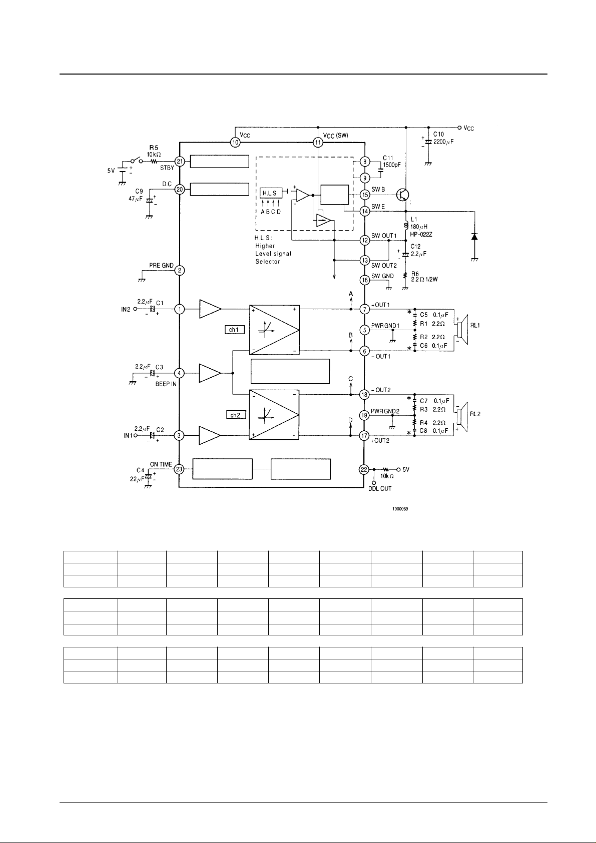
Equivalent Circuit Block Diagram
No. 5714-4/10
LA4906
Pin Voltages (At VCC= 13.2 V, with 5 V applied to STBY through a 10 kΩ resistor, using a digital voltmeter)
Pin No. 1 2 3 4 5 6 7 8
Pin IN2 Pre - GND IN1 BEEP PWR - GND 1 –OUT1 +OUT1 C
Pin voltage (V) 1.36 0 1.36 1.36 0 2.03 2.03 13.0
Pin No. 9 10 11 12 13 14 15 16
Pin C V
CC
V
CC
(SW) SW OUT1 SW OUT2 SW E SE B SW - GND
Pin voltage (V) 3.92 13.2 13.2 3.70 3.70 3.73 4.0 0
Pin No. 17 18 19 20 21 22 23
Pin +OUT2 –OUT2 PWR - GND2 D. C STAND-BY DDL OUT ON-TIME
Pin voltage (V) 2.03 2.03 0 12.1 3.21 0 2.81
Standby
switch
Switching
regulator
block
Switch
driver
Standby switch
Ripple filter
(Tokin Co. Ltd.)
(OS capacitor)
* = Polyester film capacitors
D1
SB40-05J
Flywheel diode
Amplifier output stage
Input amplifier
Input amplifier
Nonlinear amplifier/output stage
Nonlinear amplifier/output stage
TR1
Switching transistor
2SD1668, class S
Muting circuit used
at power on
Popping noise
prevention circuit
Power supply/ground shorting
protection circuit
Overvoltage/thermal
protection circuit
Beep amplifier
*
*
4 to 2 Ω
4 to 2 Ω
Page 5
No. 5714-5/10
LA4906
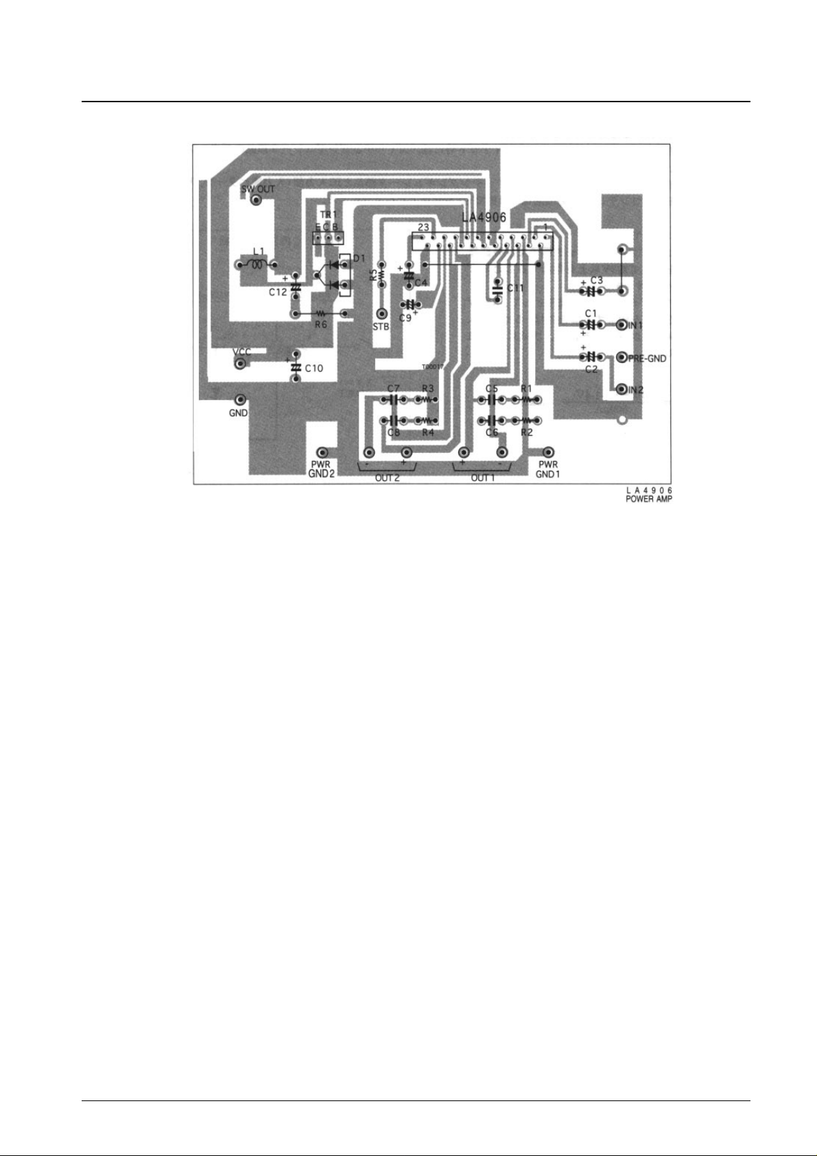
Sample Printed Circuit Board
1. External component descriptions
C1 and C2
· Input capacitors. A value of 2.2 µ F is recommended for these capacitors. Note that the low-frequency area
characteristics can be adjusted by changing fL, which is determined by the values of C1 and C2. However, due to
impulse (pop) noise considerations, the value of C1 and C2 should not exceed 3.3 µF when C4 is 22 µF.
C3
· Beep amplifier input capacitor. A value the same as that of C1 and C2 is used. If the beep function is not used, connect
the beep input to PRE-GND through C3.
C4
· Set the amplifier turn-on time. A value of 22 µF is recommended. (This will result in a turn-on time of about 0.7
second.) The on time is proportional to the value of this capacitor, and any value may be used. However, due to
impulse (pop) noise considerations, a value of 22 µF or larger should be used.
C5, C6, C7, and C8
· Oscillation prevention capacitors. Polyester film (Mylar) capacitors with good temperature characteristics must be used.
(These are used together with R1, R2, R3, and R4.) We recommend values of 0.1 µ F or higher for these capacitors
since the stability will differ somewhat depending on the printed circuit board layout actually used.
C9
· Decoupling capacitor (ripple filter)
C10
· Power-supply capacitor
C11
· Oscillation prevention capacitor for the switching regulator. A value of 1500 pF is recommended.
C12
· Switching regulator output smoothing capacitor. The LA4906 adopts a self-excited switching regulator technique. The
value of this capacitor must be optimized, since it influences both the self-excitation stability and the regulator
efficiency. We recommend using a 2.2-µ F 25-V OS (Organic Semiconductor) capacitor with a low series resistance
and good temperature characteristics. Note that for the same reason a 2.2-Ω 1/2-W resistor should be used for the
associated resistor R6.
R5
· Standby switch current limiter resistor. A value of 10 kΩ is recommended. (When the voltage applied to the standby
switch is in the range 3 to 13.2 V.) Note that this resistor cannot be removed from this circuit.
Page 6
See the “Standby Function” section elsewhere in this document.
TR1
· External switching transistor. The 2SD1668 (rank S) is recommended.
If the application supports a load resistance RL of 4 Ω, a 2SD1667 (rank S) may be used. A heat sink must be provided
for this transistor, as well as for the IC itself.
D1
· Flywheel diode used to absorb energy from the coil. The SB40-05J, which is a Schottky barrier diode with a low VF, is
recommended.
If the application supports a load resistance RL of 4 Ω, an SB10-05A2 may be used. A heat sink must be provided for
this diode, as well as for the IC itself.
L1
· The Tokin Co., Ltd.-made HP-022Z [180 µH] (or the HP-011Z [200 µH] for 4-Ω applications) is recommended.
2. IC internal characteristics and other notes
Switching regulator
· The LA4906 includes a signal-following self-excited switching regulator to reduce power dissipation. The selfexcitation frequency with no input signal is about 100 kHz.
· To avoid spurious signal interference within the end product case, it is desirable to separate the tuner block from the
amplifier block by as far as possible. When designing the printed circuit board pattern, make the lines associated with
the switching regulator external components as short and as wide as possible.
· To prevent degradation of the LA4906 characteristics, separate the switching regulator external components from the
IC inputs (the input block pattern, the input capacitors, and the beep amplifier capacitor) by at least 1.5 cm.
No. 5714-6/10
LA4906
Standby function
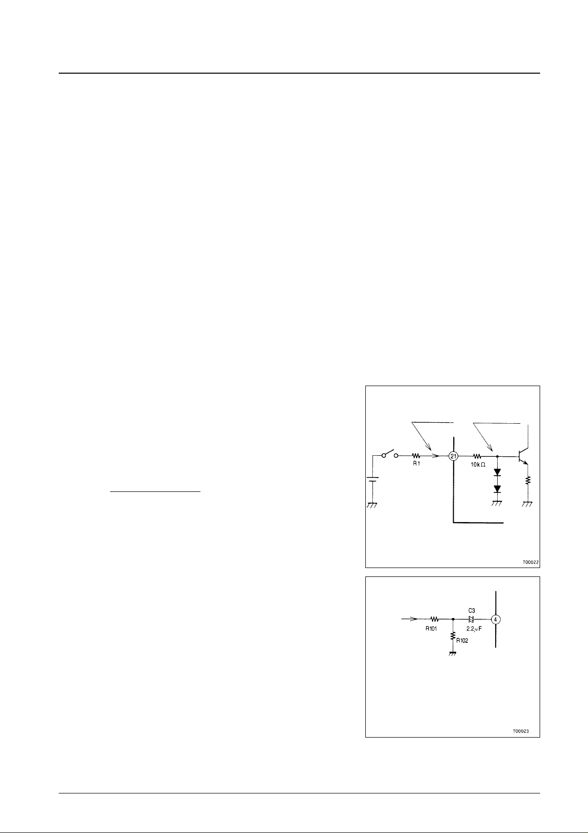
· Pin 21 is the standby switching pin. The amplifier is turned on by applying
a voltage of over 3 V to pin 21 through an external resistor (R1).
· If the standby switch applied voltage will exceed 13.2 V, then the current
flowing into pin 5 must be held to under 500 µ A. Use the following
formula to determine the value of R1 that meets this condition.
R1 =
applied voltage – 1.4 V
– 10 kΩ
500 µA
BEEP pin (pin 4)
· If the BEEP pin is used, use the smallest value of R102 (see figure)
possible (but note that this value must be under 100 Ω) to prevent
degradation of the IC's output noise voltage (VNO) characteristics.
Protection circuits
· The LA4906 includes an on-chip thermal protection circuit to prevent
destruction of or damage to the IC if abnormal heating occurs. If, due to
an inadequate heat sink or other reason, the IC junction temperature (Tj)
reaches or exceeds 160°C, the output is gradually attenuated by the
operation of the thermal protection circuit.
·
The overvoltage protection circuit operates if the VCCvoltage exceeds 20 V.
· While the LA4906 includes a power supply/ground short protection
circuit, it does not include a load shorting protection circuit. The idea
behind this design is that the thermal shutdown protection circuit will
protect the IC itself if the load is shorted. However, since a load short will
also cause temperature increases in the external transistor and coil, care is
required in handling this case.
Other notes
· Pin 22 is not connected electrically to any other points within the package.
Pin 21 IC Internal Equivalent Circuit
Applied standby
voltage
500 µA or less
Beep signal
About 1.4 V (2VBE)
Page 7
No. 5714-7/10
LA4906
Quiescent current, I
CCO
– mA
Output power, P
O
– W
Output pin voltage, V
N
– V
Output power, P
O
– W
Total harmonic distortion, THD – %
Response – dB
Output power, P
O
– W
Total harmonic distortion, THD – %
Total harmonic distortion, THD – %
Supply voltage, VCC–V
Overvoltage
protection circuit
operation
Supply voltage, VCC–V
Output power, PO– W
Input frequency, f – Hz
Input frequency, f – Hz
Output power, PO– W
Supply voltage, VCC–V
Input level, V
IN
– mV rms
Both
channels
operating
Both
channels
operating
Both
channels
operating
Both
channels
operating
Both
channels
operating
Both
channels
operating
I
O
peak exceeded
I
O
peak exceeded
Page 8
No. 5714-8/10
LA4906
Output power, P
O
– W
Channel separation, CHsep – dB
Ripple rejection ratio, SVRR – dB
Ripple rejection ratio, SVRR – dB
Power dissipation, Pd – W
Output noise voltage, V
NO
– mV rms
Ripple rejection ratio, SVRR – dB
Current drain, I
CC
– A
Input frequency, f – Hz
Input resistance, Rg – Ω
Ripple frequency, f
R
– Hz
Output power, P
O
– W
Output power, PO– W
Power supply ripple current voltage, V
CCR
– Vrms
Supply voltage, VCC–V
Input frequency, f – Hz
Both
channels
operating
Both
channels
operating
Both
channels
operating
Using a 1-µF
power-supply
capacitor
Using a 1-µF
power-supply
capacitor
Using a 1-µF power-supply
capacitor
Calculate SVRR from the
following formula:SVRR = 20 log
(VO/VCCR)
Pd for the IC itself
Pd for the external
transistor
Page 9
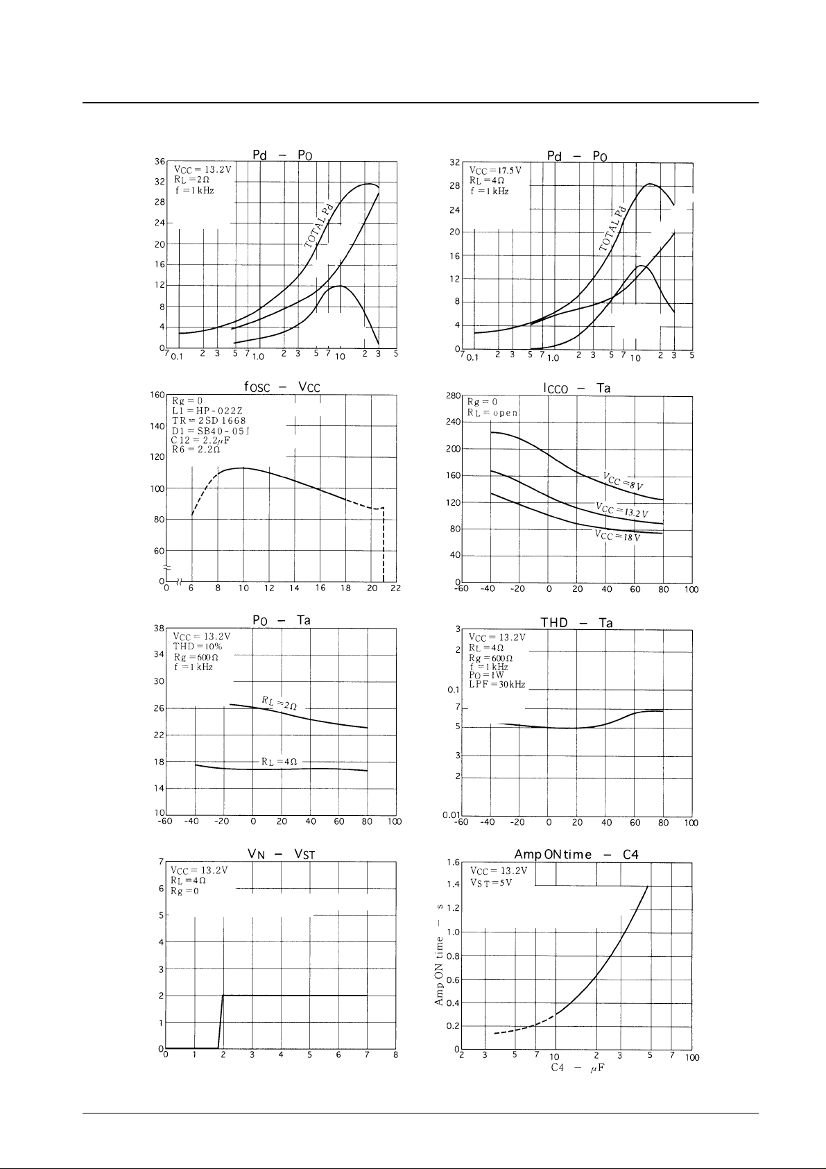
No. 5714-9/10
LA4906
With VST applied to pin 21 through a
10-kΩ resistor)
· The time until the amplifier turns on
after VSTis applied
Power dissipation, Pd – W
Power dissipation, Pd – W
Quiescent current, I
CCO
– mA
Total harmonic distortion, THD – %
Regulator oscillator frequency, f
OSC
– kHz
Output power, P
O
– W
Output pin voltage, V
N
– V
Output power, PO– W
Supply voltage, VCC– V
Ambient temperature, Ta – °C
Applied standby pin voltage, VST– V
Ambient temperature, Ta – °C
Ambient temperature, Ta – °C
Output power, P
O
– W
Both
channels
operating
Both
channels
operating
Both
channels
operating
Both
channels
operating
Pd for the
external
transistor
Pd for the
external
transistor
Pd for the IC itself
Pd for the IC itself
(Tokin Co., Ltd.)
(OS capacitor)
In the recommended circuit
With VST applied to the standby pin
(pin 21) through a 10-kΩ resistor
Page 10

No. 5714-10/10
LA4906
This catalog provides information as of July, 1997. Specifications and information herein are subject to change
without notice.
■ No products described or contained herein are intended for use in surgical implants, life-support systems, aerospace
equipment, nuclear power control systems, vehicles, disaster/crime-prevention equipment and the like, the failure of
which may directly or indirectly cause injury, death or property loss.
■ Anyone purchasing any products described or contained herein for an above-mentioned use shall:
➀ Accept full responsibility and indemnify and defend SANYO ELECTRIC CO., LTD., its affiliates, subsidiaries and
distributors and all their officers and employees, jointly and severally, against any and all claims and litigation and all
damages, cost and expenses associated with such use:
➁ Not impose any responsibility for any fault or negligence which may be cited in any such claim or litigation on
SANYO ELECTRIC CO., LTD., its affiliates, subsidiaries and distributors or any of their officers and employees
jointly or severally.
■ Information (including circuit diagrams and circuit parameters) herein is for example only; it is not guaranteed for
volume production. SANYO believes information herein is accurate and reliable, but no guarantees are made or implied
regarding its use or any infringements of intellectual property rights or other rights of third parties.
 Loading...