

Page 1
Ordering number: EN3680C
Monolithic Linear IC
LA4485
5 W, Two-channel Power Amplifier with Very Few
External Parts
Overview
The LA4485 is a 5 W, two-channel power amplifier IC that
requires a minimum of external parts, making it ideal for radio
cassette players and car stereo equipment.
The LA4485 eliminates the need for bootstrap capacitors,
negative feedback capacitors, and oscillation prevention CR
parts, all of which were necessities for power ICs previously.
All of these functions are now on chip, keeping the number of
external parts to an absolute minimum. The LA4485 is part of
the Power (Stylish Power) Series, and supports two modes:
dual and BTL.
Features
.
5W×2 output power in dual mode, and 15 W in BTL mode
.
Minimum external parts for the Power Series count:
4 or 5 parts in dual mode; 3 or 4 parts in BTL mode
.
Protection circuits
Overvoltage protection
Thermal protection
DC output short-circuit protection (to V
.
Circuitry designed to handle +VCCapplied to the outputs
.
Pop noise reduction
.
Standby switch
.
Muting function
and to GND)
CC
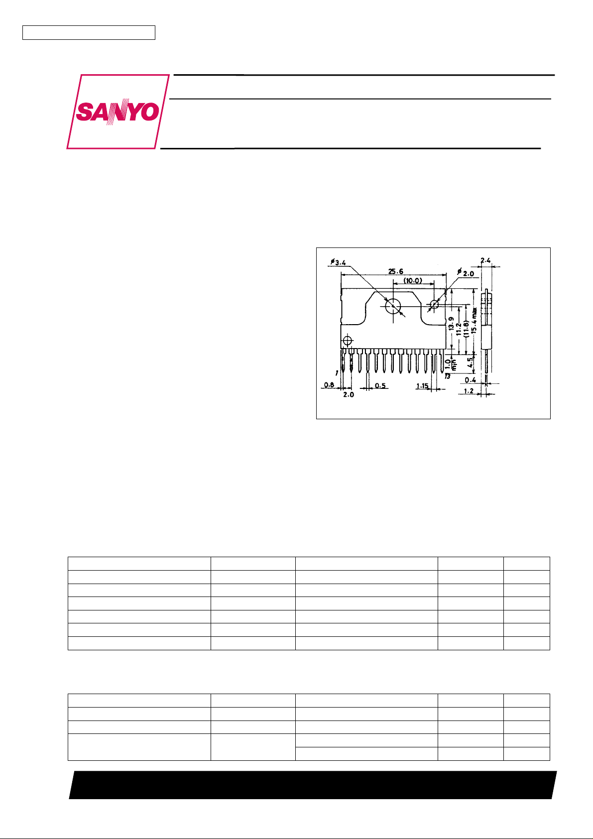
Package Dimensions
unit : mm
3107-SIP13H
[LA4485]
SANYO : SIP13H
Specifications
Maximum Ratings at Ta = 25°C
Parameter Symbol Conditions Ratings Unit
Maximum supply voltage V
Surge supply voltage V
Peak output current I
Allowable power dissipation Pd max With infinite heat sink 15 W
Operating temperature Topr –30 to +80 °C
Storage temperature Tstg –40 to +150 °C
*: By the π type B check point method.
max No signal 24 V
CC
surge * Based on the JASO standard 50 V
CC
peak Per channel 3.3 A
O
Operating Conditions at Ta = 25°C
Parameter Symbol Conditions Ratings Unit
Recommended supply voltage V
Supply voltage range V
Recommended load resistance range R
CC
CC
op Must not be over package Pd 7.5 to 18 V
L
Dual 2 to 8 Ω
BTL 4to8 Ω
13.2 V
SANYO Electric Co.,Ltd. Semiconductor Bussiness Headquarters
TOKYO OFFICE Tokyo Bldg., 1-10, 1 Chome, Ueno, Taito-ku, TOKYO, 110 JAPAN
73096HA(II)/D2893TS/9041TS No.3680-1/20
Page 2
LA4485
Operating Characteristics at Ta = 25°C, VCC= 13.2 V, RL=4Ω,Rg=600Ω,f=1kHz, Dual
Parameter Symbol Conditions min typ max Unit
Standby current Ist Pin 9 to GND, Standby switch OFF 10 µA
Quiescent supply current I
Voltage gain
Output power
CCO
VG1 Dual: V
VG2 BTL: V
P
O
P
O
Total harmonic distortion THD P
Channel separation CH sep V
Output noise voltage V
NO
Ripple rejection ratio SVRR
*: PO1 = 6 W (typ) when VCC= 14.4 V
Voff ± 250 mV for BTL-mode
Rg = 0 40 80 160 mA
= 0 dBm 43 45 47 dB
O
= 0 dBm 51 dB
O
1* Dual: THD = 10% 4 5 W
2 BTL: THD = 10% 11 15 W
= 1 W 0.15 0.8 %
O
= 0 dBm, Rg = 0 45 55 dB
O
Rg = 0, 20 Hz to 20 kHz bandpass filter 0.15 0.5 mV
Rg = 0, 20 Hz to 20 kHz bandpass filter,
f
= 100 Hz, VR= 0 dBm, decoupling capacitor
R
connected
40 50 dB
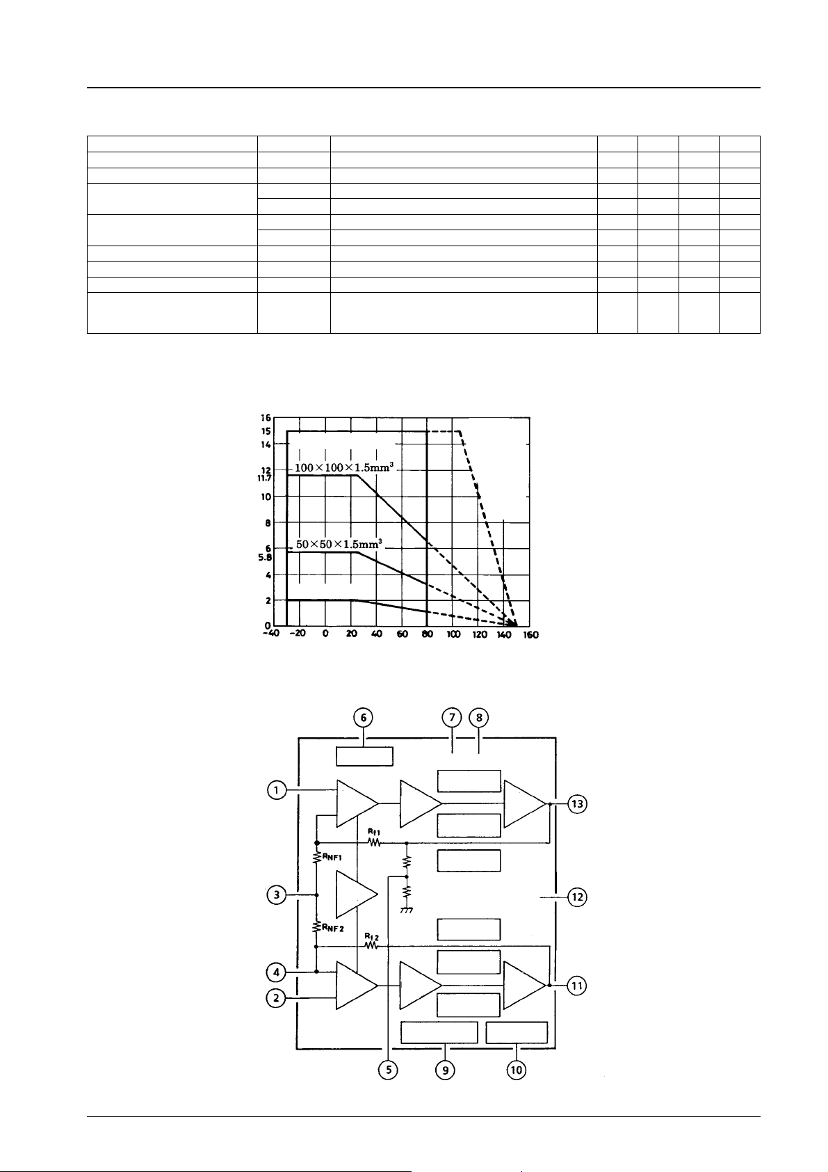
Pd max – Ta
Al heat sink
mounting
Infinite heat sink
conditions
Mounting
torque
39 Nvcm.
Flat washer
with silicone
grease
applied
No heat sink
Allowable power dissipation, Pd max – W
Ambient temperature, Ta – °C
Equivalent Circuit Block Diagram
CH1 IN
Small signal GND
BTL IN
CH2 IN
FILTER
Input
amp
CH1
REF
amp
Input
amp
CH2
Filter
Large signal
V
CC
Output-to-ground
short-circuit
protection
Pre
drive
amp
Output-to-supply
short-circuit
protection
Thermal shutdown
Output-to-supply
short-circuit
Pre
drive
amp
protection
Output-to-ground
short-circuit
protection
Standby switch
Small signal
V
CC
protection
Overvoltage
protection
Output
amp
Output
amp
Mute
CH1 OUT
Large signal GND
CH2 OUT
BTL OUT
STANDBY
MUTE
No.3680-2/20
Page 3
LA4485
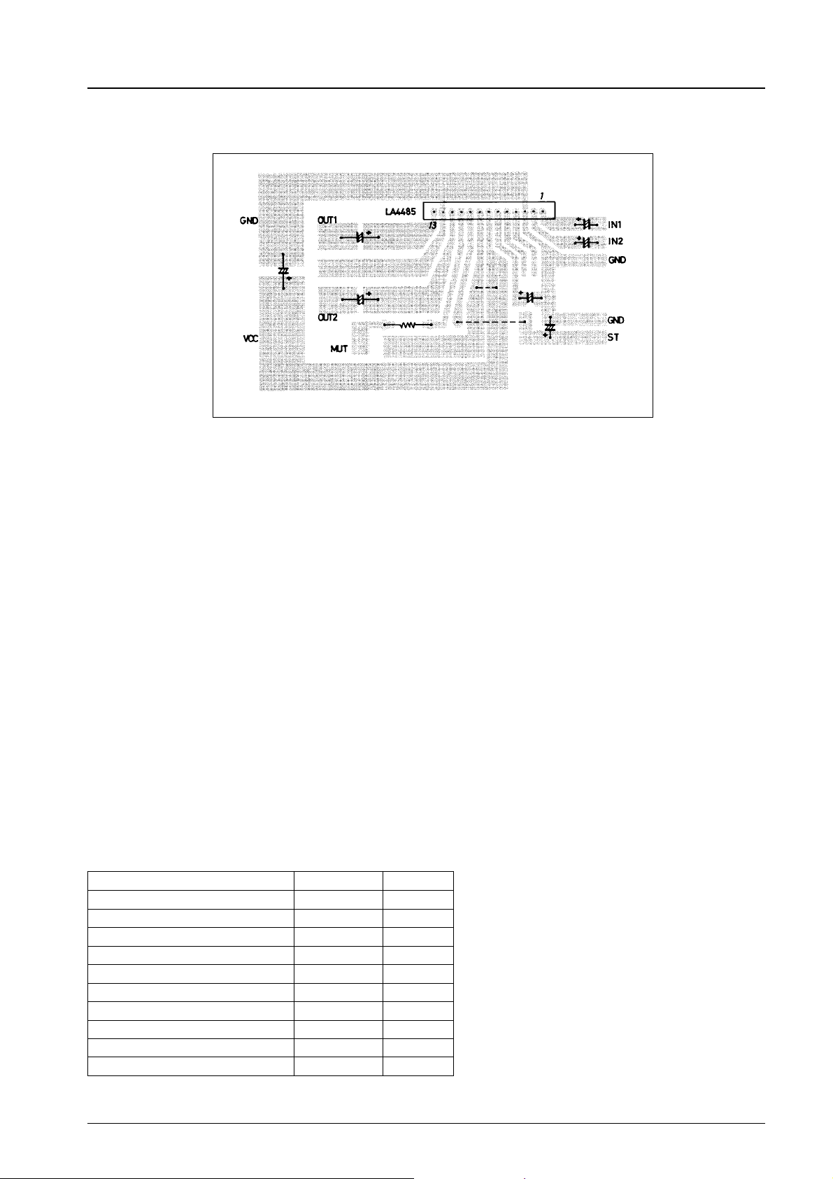
Recommended LA4485 External Parts Arrangement (Dual-mode)
95.0 × 67.0 mm
2
IC Usage Notes
Maximum ratings
Care must be taken when operating the LA4485 close to the maximum ratings as small changes in the operating conditions can
cause the maximum ratings to be exceeded, thereby breakdown will be caused.
Printed circuit board connections
Care must be taken when designing the circuit of printed board so as not to form feedback loops, particularly with the small-signal
and large-signal ground connections.
Notes on LA4485 heatsink mounting
1. Mounting torque must be in the range 39 to 59 Nvcm.
2. The spacing of the tapped holes in the heatsink must match the spacing of the holes in the IC tab.
3. Use screws with heads equivalent to truss head machine screws and binding head machine screws stipulated by JIS for the
mounting screws. Furthermore, washers must be used to protect the surface of the IC tab.
4. Make sure that there is no foreign matter, such as cutting debris, between the IC tab and the heatsink. If a heat conducting
compound is applied between the contact surfaces, make sure that it is spread uniformly over the entire surface.
5. Because the heatsink mounting tab and the heatsink are at the same electric potential as the chip’s GND (large signal GND),
care must be taken when mounting the heatsink on more than one device.
6. The heatsink must be mounted before soldering the pins to the PCB.
Comparison of External Parts Required
External parts Existing device LA4485
Output coupling capacitors Yes Yes
Input coupling capacitors Yes Yes
Bootstrap capacitors Yes No
Feedback capacitors Yes No
Filter capacitor Yes Optional
Phase compensating capacitor Yes No
Oscillation-quenching mylar capacitors Yes No
Oscillation-quenching resistors Yes No
Others No Optional
Total (for dual-mode) 15 to 16 parts 4 to 6 parts
Note: Supply capacitors, contained within the power IC, are not counted in both existing and new devices.
No.3680-3/20
Page 4
LA4485
Operating Pin Voltages at VCC= 13.2 V
Pin No. Name Function Pin voltage (Reference value)
1 CH1 IN Channel 1 input. 1.4 V (2 V
2 CH2 IN Channel 2 input. 1.4 V (2 V
3 SS GND Small-signal ground 0 V
4 BTL IN BTL-mode feedback input. 45 mV
5 BTL OUT BTL-mode feedback output. 3.1 V (61/4 V
6 FILTER Filter capacitor connection. 6.6 V (61/2 V
7LSV
8SSV
9 STANDBY Standby control input. 5 V
10 MUTE Mute control input. 0 V
11 CH2 OUT Channel 2 output. 6.3 V
12 LS GND Large-signal ground 0 V
13 CH1 OUT Channel 1 output. 6.3 V
Large-signal supply 13.2 V (VCC)
CC
Small-signal supply 13.2 V (VCC)
CC
Note: Each pin is so arranged lest the IC should be broken even if inserted reversely.
BE
BE
)
)
)
CC
)
CC
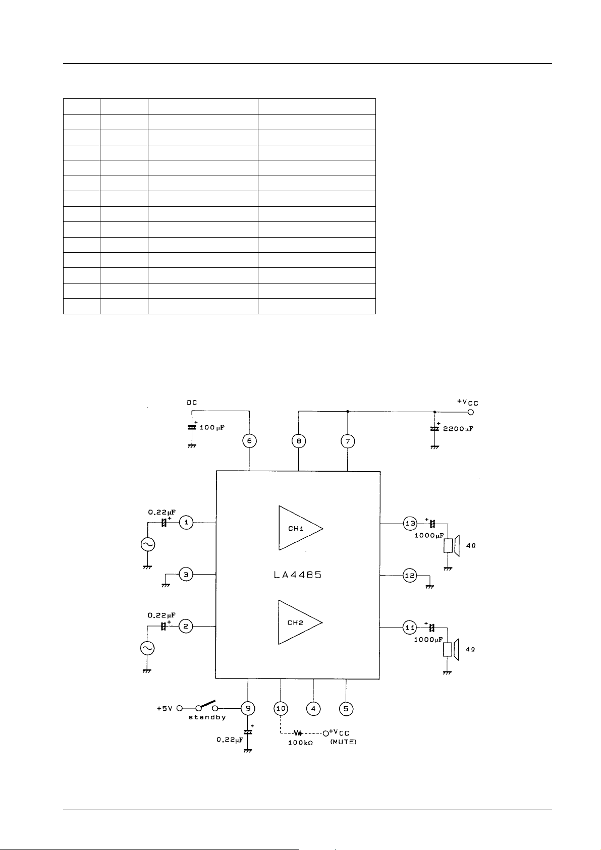
LA4485 Sample Application Circuit
No.3680-4/20
Page 5
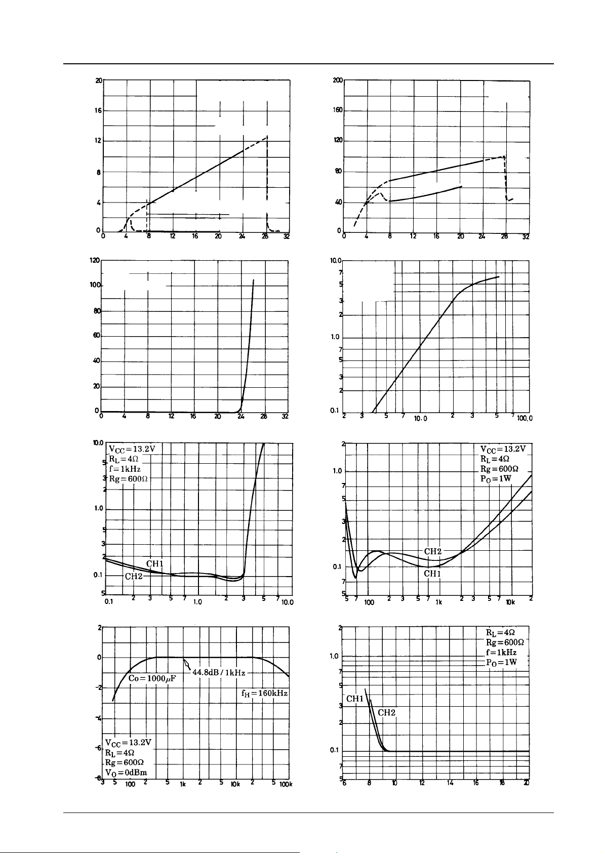
LA4485
–V
N
Output pin voltage, V
Supply voltage, VCC–V
CVCC= 0.15 µF (mylar)
Rg = 0
Standby to GND
VN–V
CC
=4Ω(dual)
R
L
Rg = 0 standby + 5 V
Overvoltage cutoff
VCC= 7.5 V
Cutoff for waveform carrying signal
Muting on
lst–V
CC
–mA
CCO
Quiescent supply current, I
VCC= 13.2 V
R
f = 1 kHz
Rg = 600 Ω
–W
O
L
I
CCO–VCC
Muting on
Supply voltage, VCC–V
P
=4Ω
O–VIN
=4Ω
R
L
Rg=0
I
CCO
Standby current, Ist – µA
Supply voltage, VCC–V
THD–P
O
Total harmonic distortion, THD – %
Output power, PO–W
f Response
Output power, P
Input voltage, VIN–mV
THD–f
Total harmonic distortion, THD – %
Frequency,f–Hz
THD–V
CC
Response – dB
Total harmonic distortion, THD – %
Frequency,f–Hz
Supply voltage, VCC–V
No.3680-5/20
Page 6
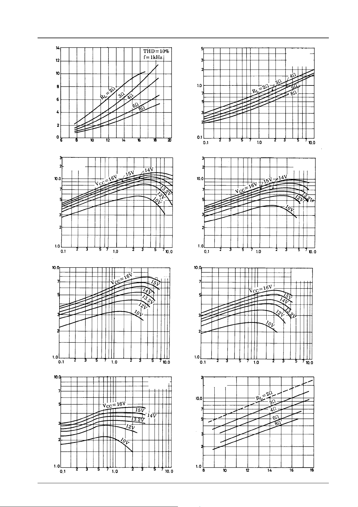
LA4485
–W
O
Output power, P
Dual
RL=2Ω
PO–V
CC
Supply voltage, VCC–V
Pd–P
O
(2CH) – A
Current drain, I
CC
I
CC–PO
Dual
Rg = 600 Ω
f = 1 kHz
Output power, PO(1CH) – W
Pd–P
O
Dual
RL=3Ω
Power dissipation, Pd (2CH) – W
Power dissipation, Pd (2CH) – W
Output power, PO(1CH) – W
Pd–P
O
Output power, PO(1CH) – W
Pd–P
O
Dual
R
=4Ω
L
Dual
RL=8Ω
Power dissipation, Pd (2CH) – W
Power dissipation, Pd (2CH) – W
Output power, PO(1CH) – W
Pd–P
Output power, PO(1CH) – W
Pd max – V
Dual
Ta = 25°C
O
Dual
RL=6Ω
CC
Power dissipation, Pd (2CH) – W
Output power, PO(1CH) – W
–W
Allowable power dissipation, Pd max (2CH)
Supply voltage, VCC–V
No.3680-6/20
Page 7

LA4485
CH sep – f
Leakage from CH2 to CH1
Leakage from CH1 to CH2
Channel separation, CH sep – dB
Frequency,f–Hz
SVRR – V
CC
Ripple rejection ratio, SVRR – dB
Supply ripple voltage, VR–mV
SVRR – V
SVRR – f
R
R
Ripple rejection ratio, SVRR – dB
–mA
CCO
Quiescent current, I
–W
O
Supply voltage, VCC–V
I
–Ta
CCO
Ambient temperature, Ta – °C
PO–Ta
Ripple rejection ratio, SVRR – dB
–V
N
Output pin voltage, V
Ambient temperature, Ta – °C
VCC= 13.2 V
R
=4Ω
L
BPF=20Hzto20kHz
–mV
Rg=0→0.12 mV
NO
Ripple frequency, fR–Hz
V
–Ta
N
V
–Rg
NO
Temperature characteristic due to output capacitor
CO= 1000 µF
Output power, P
Ambient temperature, Ta – °C
Output noise voltage, V
Source resistance, Rg – Ω
No.3680-7/20
Page 8
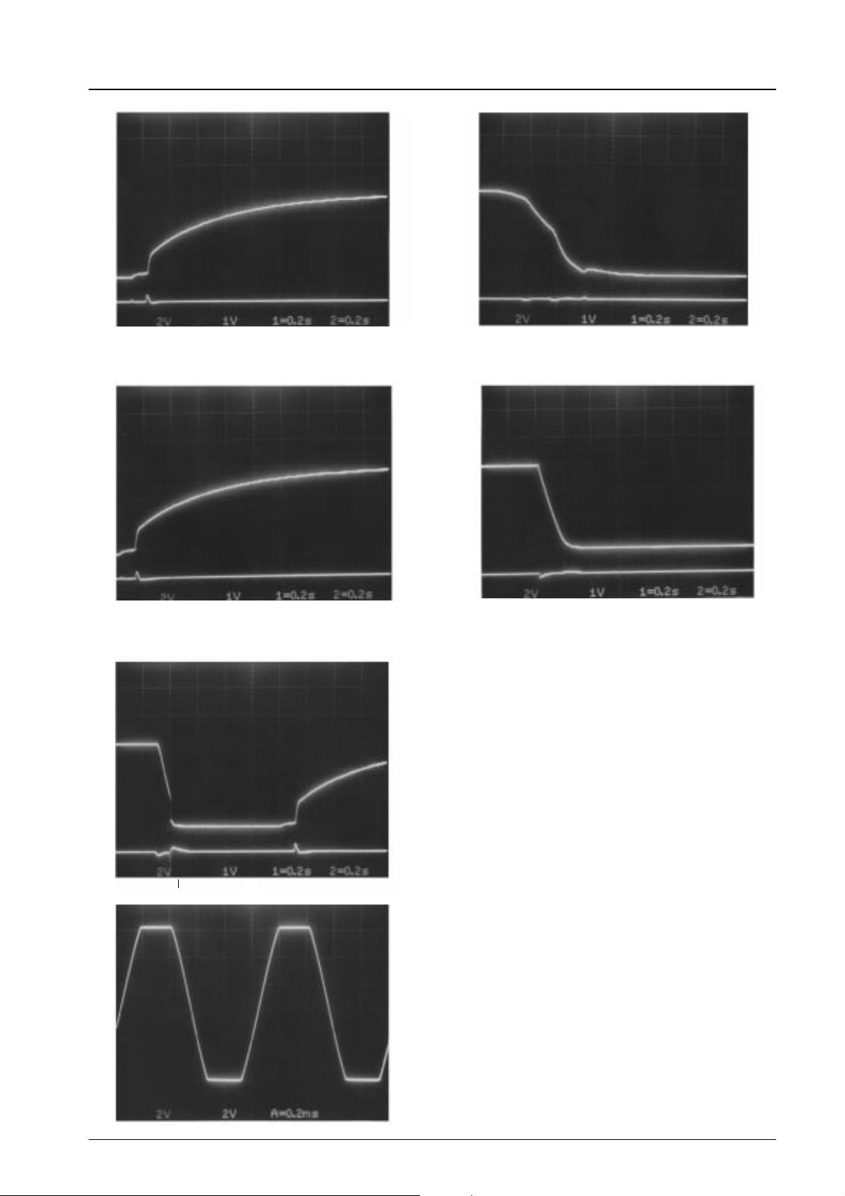
LA4485
Output
DC trace
Speaker
terminal
VCC= 13.2 V, standby supply +5 V,
R
=4Ω,Rg=0
L
Main switch ON/OFF test
Output
DC trace
Speaker
terminal
V
= 13.2 V, standby supply +5 V,
CC
R
=4Ω,Rg=0
L
Standby switch ON/OFF text
VCC= 13.2 V,
R
=4Ω,
L
Rg = 0,
Mute ON/OFF
→ Switching noise decreases as CIN= 0.22 µF (Input) is increased. (ex. 2.2 µF)
VCC= 13.2 V,
R
=4Ω,
L
Rg = 600 Ω,
THD = 10%,
f = 1 kHz,
Output DC waveform
No.3680-8/20
Page 9
LA4485
Dual-mode Operation Notes
.
Use the input capacitor CINin the range of 0.22 µF to 1.0 µF.
Parameter CIN= 0.22 µF CIN= 1.0 µF
Start-up time (ts) 0.15 s 0.25 s
Attack noise when using the muting function Somewhat noticeable Good
Speaker turn-ON transient noise increased significantly when CINis 2.2 µF or greater.
.
The DC (filter) capacitor should be 100 µF or greater.
Parameter 100 µF or less 100 µF or more
Standby-off output capacitor
discharge circuit
Ripple rejection ratio (SVRR)
V
rise rate when main or
N
standby is turned ‘‘on’’
Note:
*1. Slow as a result of natural discharge.
*2. Approximately 0.3 seconds as a result of forced discharge.
.
Use the standby supply capacitor in the range of 0.22 µF to 0.47 µF.
The V
or greater. If the standby function is not used, this capacitor must be removed and pin 9 must be pulled up to the power supply.
.
The output capacitor’s recommended value for COis 1,000 µF.
Smaller capacitance will worsen the roll-off frequency f
.
The recommended power supply capacitor is approximately 2,200 µF, but other capacitors than 2,200 µF can be used according
to the application’s design.
Using a capacitor with this value, the load on the supply can be as high as 56 Ω while still providing good supply stability
during momentary supply glitches. Note that using a 0.15 µF capacitor can cause oscillations if the supply impedance increases.
(Example: Mild oscillation results if the power supply capacitor is open.)
trace for standby OFF changes and speaker turn-ON transient noise is increased significantly when the capacitor is 1 µF
N
*1. Does not operate.
Repeated on/off: poor
Somewhat worse
40 dB
Fast Slow
and POin a low range.
L
*2. Operates normally.
On/off: good
Good
50 dB
.
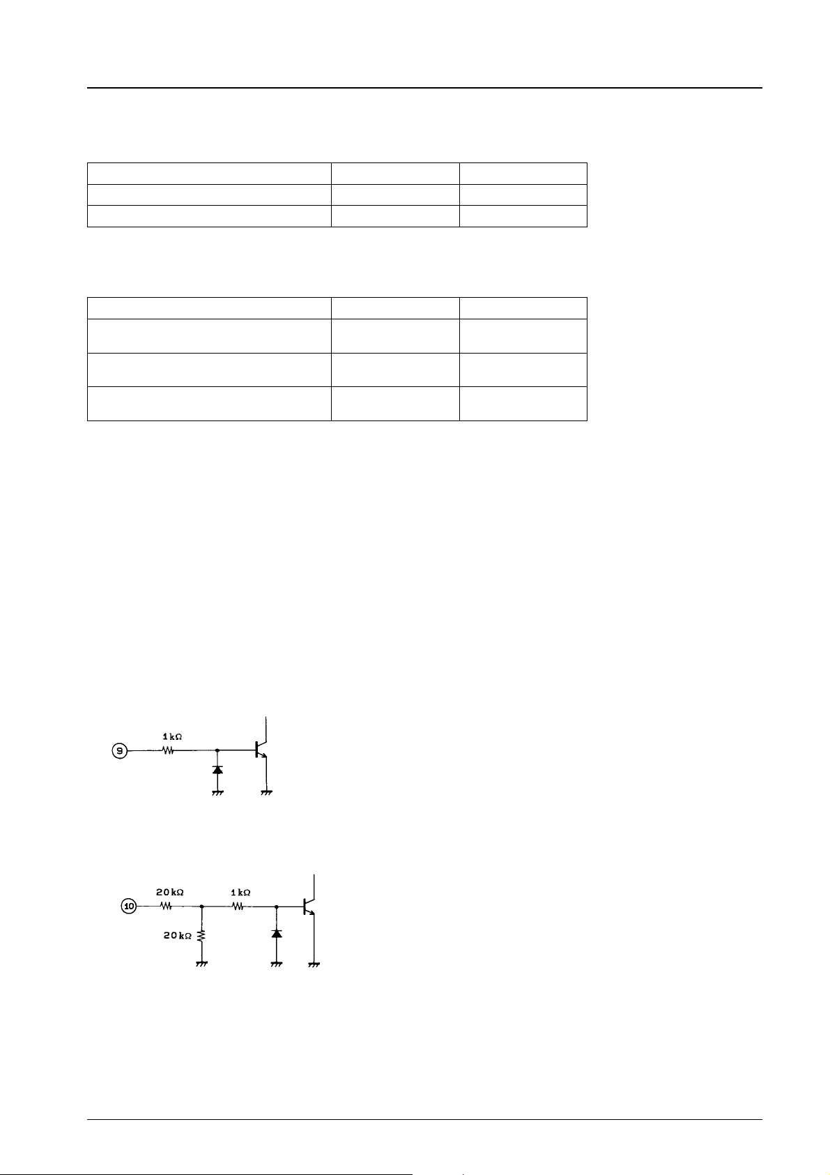
STANDBY pin 9 IC internal circuit
.
MUTE pin 10 IC internal circuit
No.3680-9/20
Page 10
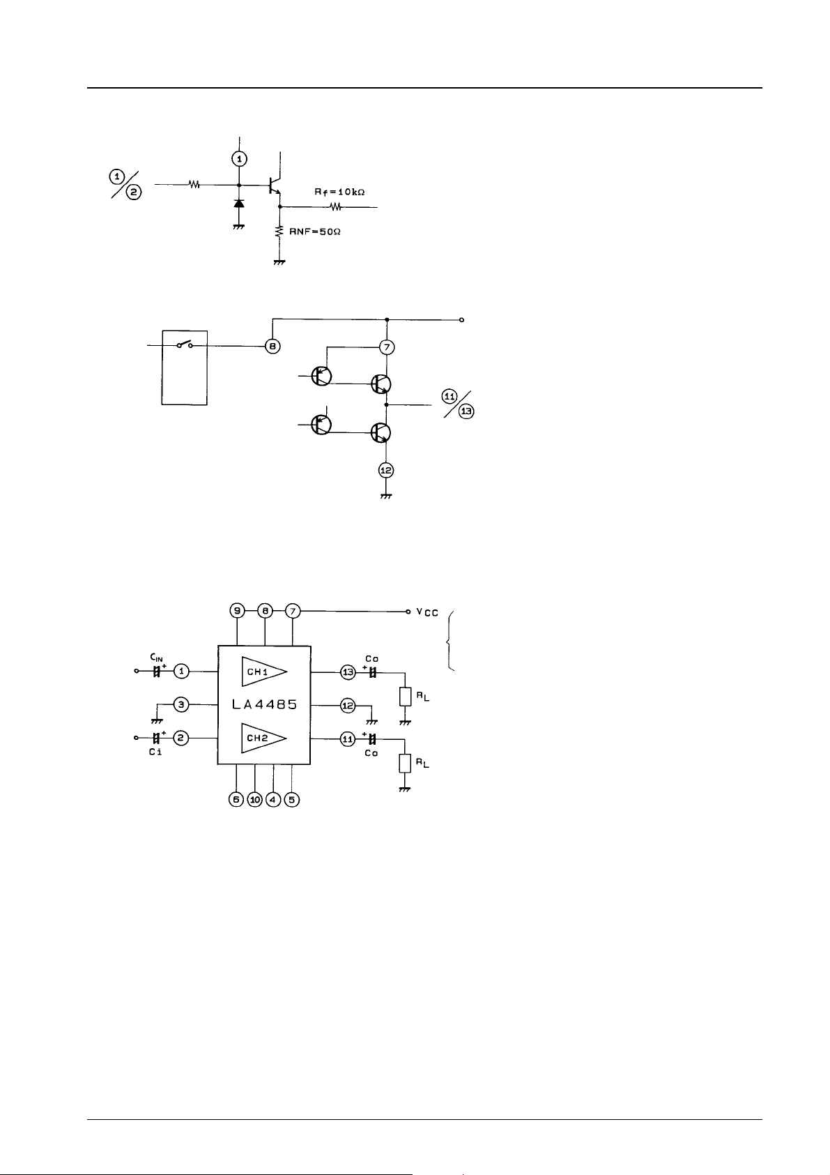
.
Input pin 1/2 IC internal circuit
.
Output pin 11/13 IC internal circuit
LA4485
SS V
Bias
Standby
line
.
The minimum configuration for dual-mode operation
CC
Driver
Driver
Upward/Downward PNP Driver Format
LS V
CC
Power
transistor
Power
transistor
LS GND
No standby function
SVRR 6 40 dB
C
= 1000 µF
O
C
= 2.2 µF
IN
(Four-point method)
No.3680-10/20
Page 11
LA4485
.
Insert capacitors of 1000 pF between each input and ground to prevent external noise.
.
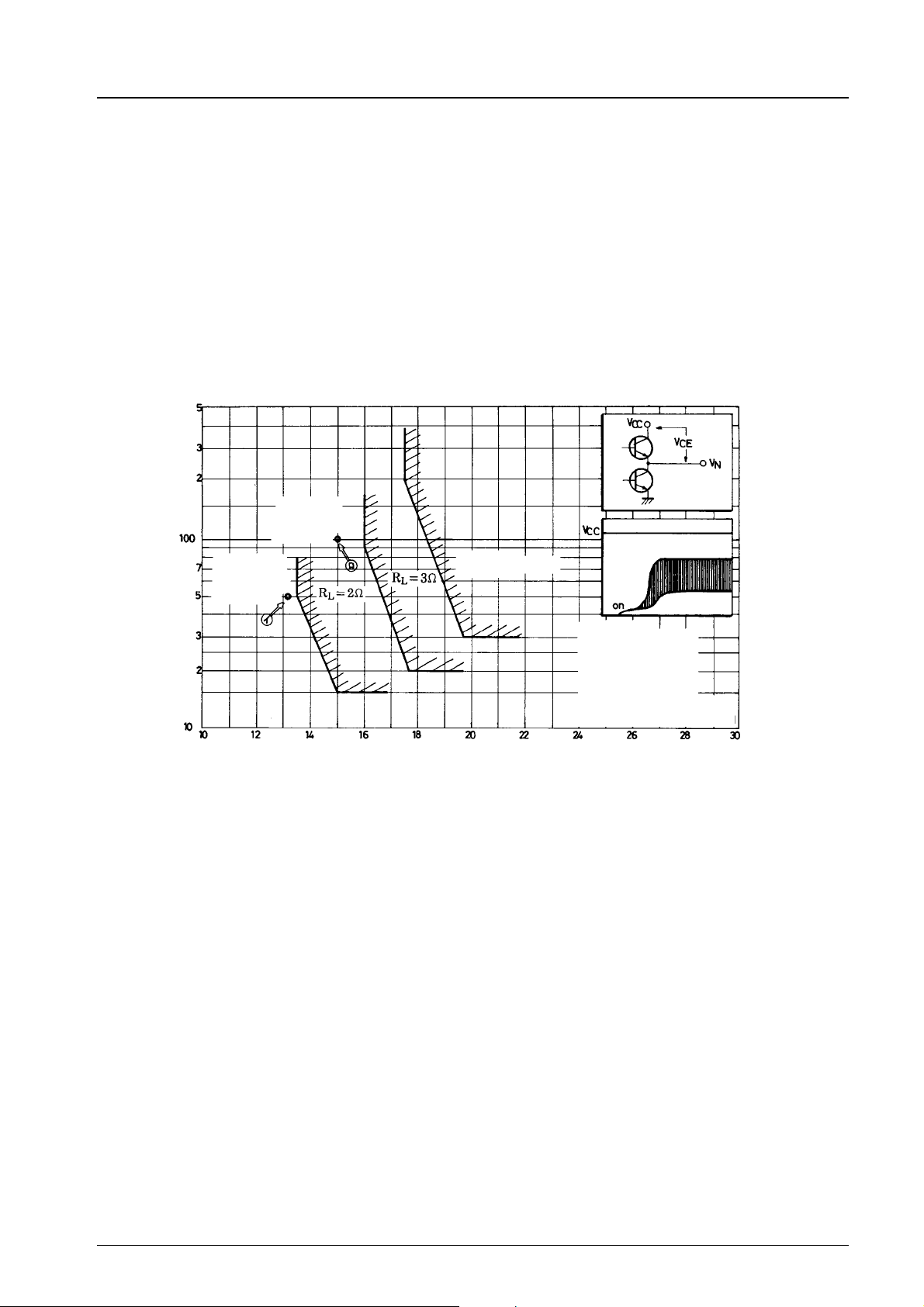
When the load (RL) or the supply voltage (VCC) is increased, turning the standby switch or the main switch on under strong
input conditions will activate the IC’s internal pseudo ASO protection circuit for the upper power transistor (V
causes output oscillations or intermittent operation (The reference area is shown in Figure 1 below). However, strong input tests
after the bias has stabilized have no problems. They also protect the upper power transistors close to the limits of ASO when all
signal switches are on. Therefore, when using this IC under these conditions, the circuit design should obey the following
condition:
Signal generation time > Start-up time of the power amplifier IC
or some other method of attaining the zero-volume condition should be adopted.
.
An undervoltage protection circuit operates when the voltage is 7.5 V or lower.
This figure shows the pseudo ASO protection area when strong signal is input, and switch is ON:
the upper power transistors have an area where V
PHOTO-2
VCC=15V
–mVrms
IN
PHOTO-1
VCC= 13.2 V
RL=2Ω
RL=3Ω
× I
CE
CP
RL=4Ω
Design center
load is caused.
× ICP). This
CE
Input voltage, V
Strong signal input after switch-ON is OK.
In BTL-mode operation, the load is R
× 2
L
Supply voltage, VCC–V
Figure 1
Dual-mode operation
f=1kHz
Dual channel drive
Non-inductive load
Ta = 25°C
Standby switch ON in a
typical application
No.3680-11/20
Page 12
LA4485
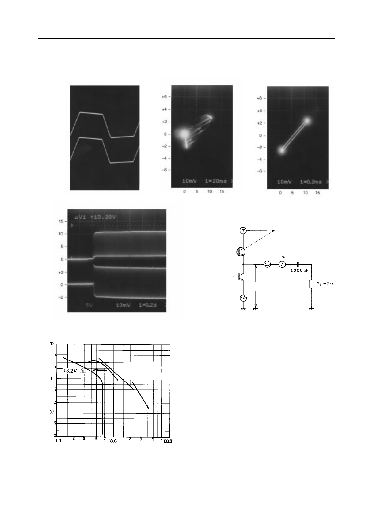
i) The operating condiations for the PHOTO-1 series in dual mode are VCC= 13.2 V, RL=2Ω,f=1kHz, VIN=50mVand
standby switch ON.
‘‘X-Y path observed within the normal area’’: checking each channel
–V
CE
Output waveforms Transition
icp – A
Power transistor
Current and voltage waveforms
CE voltage – V
↓
* Plot each point on the power
transistor ASO curve. Refer to
Figure 2.
–V
CE
icp – A V
Stabilization
Power transistor
CE voltage – V
‘‘VCC–VCE’’ added,
heavy load
I
(Y)
CP
–A
E
Emitter current, I
icp – A V
V
CE (X)
Transition Stabilization
IE–V
CB
Upper power transistor
The load line becomes more closely aligned with the
vertical axis because of the load.
Shifting load line at
start-up under
large-signal conditions
Collector-base voltage, VCB–V
Figure 2
No.3680-12/20
Page 13
LA4485
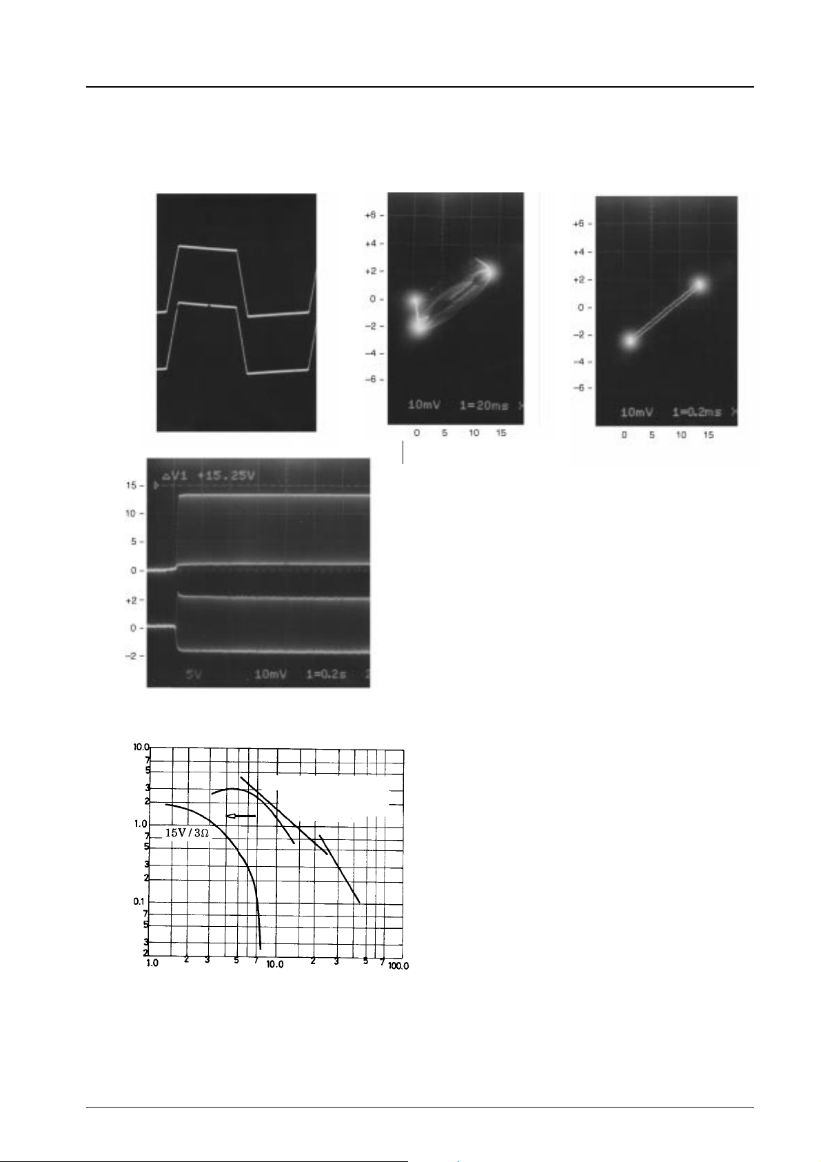
ii) The operating conditions for the PHOTO-2 in dual mode are VCC=15V,RL=3Ω,f=1kHz, VIN= 100 mV and standby
switch ON.
‘‘X-Y path observed within the normal area’’
–V
CE
Output waveforms
Current and voltage waveforms
Transition
icp – A
icp – A
Power transistor
CE voltage – V
↓
Stabilization
Power transistor
CE voltage – V
* Plot each point on the power
transistor ASO curve. Refer to
Figure 3.
icp – A V
Transition Stabilization
–A
E
Emitter current, I
Collector-base voltage, VCB–V
IE–V
Figure 3
CB
Shifting load line at
start-up under
large-signal conditions
No.3680-13/20
Page 14
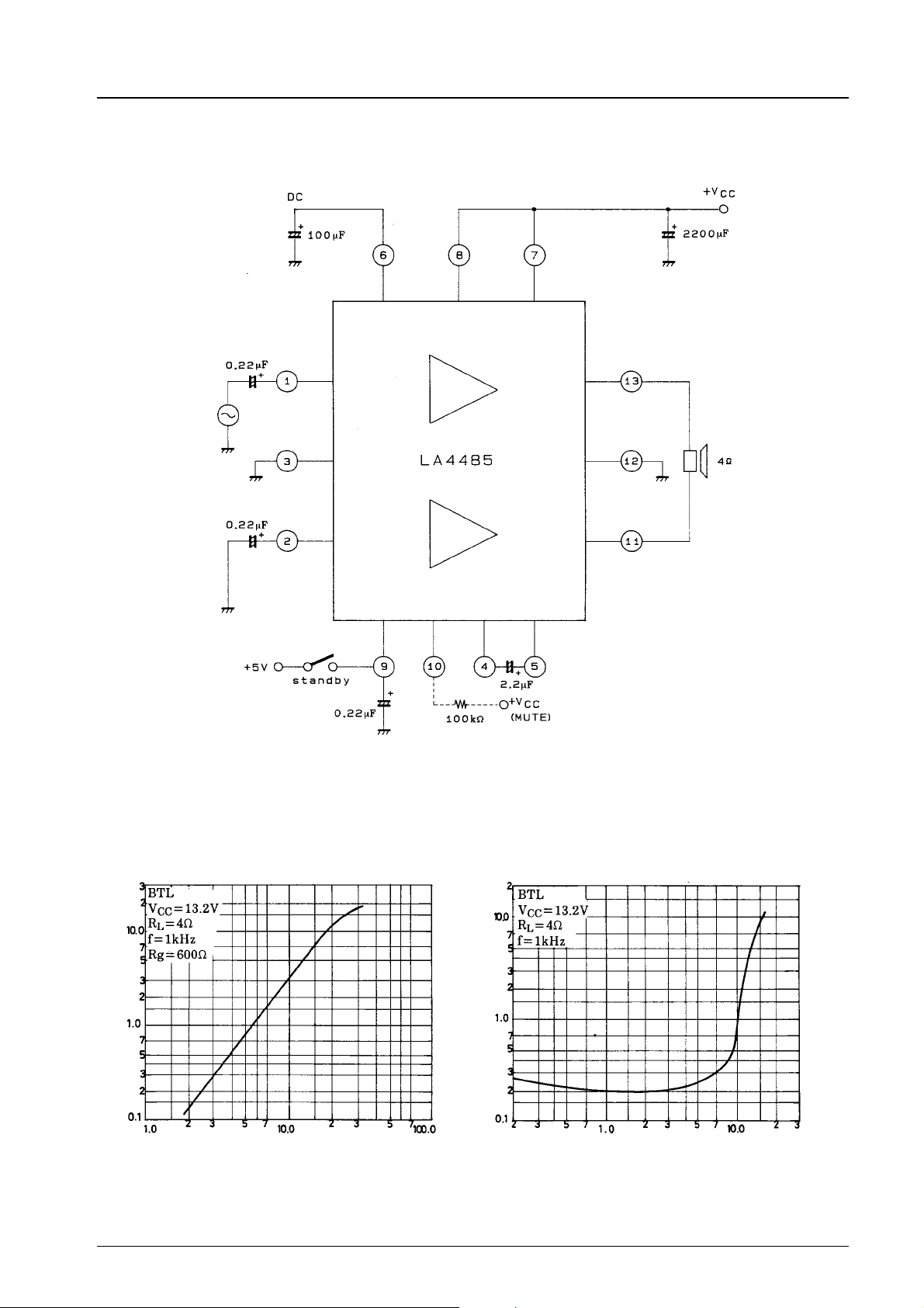
LA4485, BTL Sample Application Circuit
LA4485
Noninverting
–W
O
PO–V
Inverting
IN
THD–P
O
Output power, P
Total harmonic distortion, THD – %
Input voltage, VIN–mV
Output power, P
O
–W
No.3680-14/20
Page 15
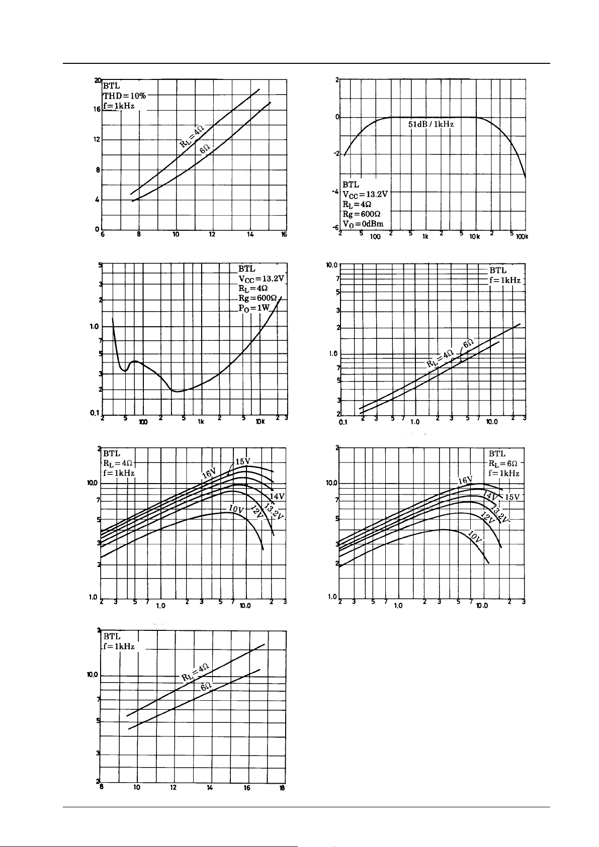
LA4485
–W
O
Output power, P
PO–V
CC
Supply voltage, VCC–V
THD–f
Response – dB
–A
CC
f Response
Frequency,f–Hz
I
CC–PO
Total harmonic distortion, THD – %
Power dissipation, Pd – W
Frequency,f–Hz
Pd–P
O
Output power, PO–W
Pd max – V
CC
Power dissipation, Pd – W
Current drain, I
Output power, PO–W
Pd–P
O
Output power, PO–W
Allowable power dissipation, Pd max – W
Supply voltage, VCC–V
No.3680-15/20
Page 16
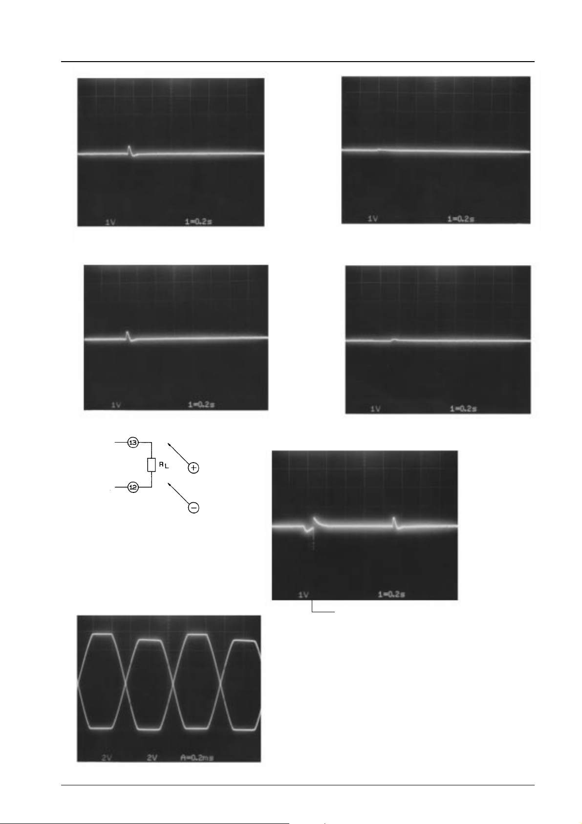
LA4485
BTL
Speaker
terminal
V
= 13.2 V, standby +5 V,
CC
R
=4Ω,Rg=0
L
Main switch ON/OFF test
BTL
Noninverting
Inverting
V
= 13.2 V, standby +5 V,
CC
R
=4Ω,Rg=0
L
Standby switch ON/OFF test
Measurement
Noninverting Inverting
Speaker
terminal
→ Note: Switching noise decreases as
BTL
V
= 13.2 V,
CC
R
=4Ω,
L
Rg = 600 Ω,
THD = 10%,
f = 1 kHz
Output DC waveform
BTL
V
CC
R
L
Rg = 0
Mute ON/OFF
C
= 0.22 µF (input) is increased. (ex. 2.2 µF)
IN
= 13.2 V
=4Ω
No.3680-16/20
Page 17
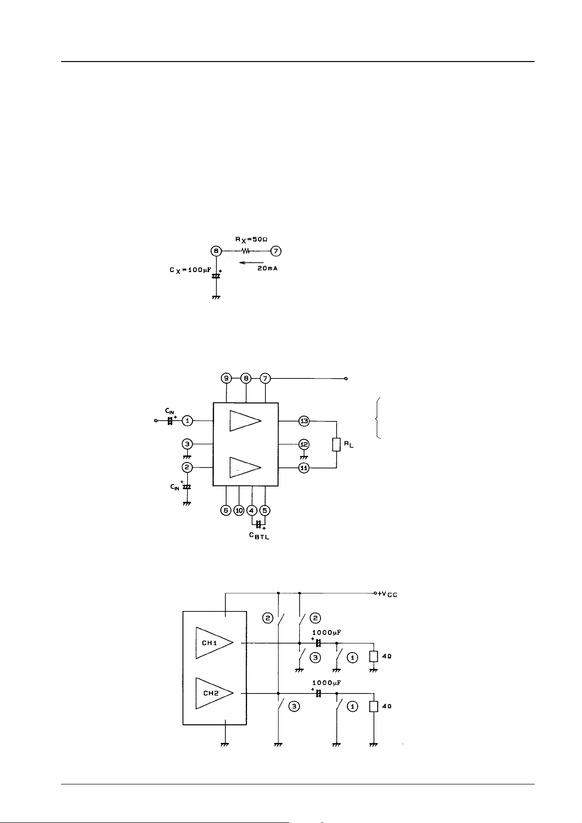
LA4485
BTL-mode Operation Notes
In BTL mode, channel 1 should be non-inverted and channel 2 should be inverted.
.
Use the input capacitor CINin the range 0.22 µF to 2.2 µF.
.
Use the standby supply capacitor in the range 0.22 µF to 1.0 µF.
When the capacitor is 2.2 µF or more, the V
.
The recommended DC (filter) capacitor is 100 µF or greater.
.
The BTL-mode coupling capacitor should be 2.2 µF.
When this capacitor is decreased, the output power is decreased. However, when this capacitor is increased, speaker
turn-ON transient noise is increased significantly.
.
In BTL mode, the ripple rejection ratio (SVRR) is approximately 40 dB.
This is because the output ripple portion of the noninverted side penetrates the BTL coupling end, so that ripple on the
inverted side is large. The following method is described as one external measure:
trace for standby-off changes, and the switching noise increases significantly.
N
SS V
CC
This measure yields an SVRR of approximately 50 dB. Note that the Rx loss voltage is approximately 1 V, and the P
about 1.0 to 1.5 W (to the 15 W level).
.
Example of minimum parts for BTL operation
Noninverting
Inverting
LS V
CC
No standby function
SVRR 6 40 dB
C
= 2.2 µF
IN
C
= 2.2 µF
BTL
(Three point method)
O
loss is
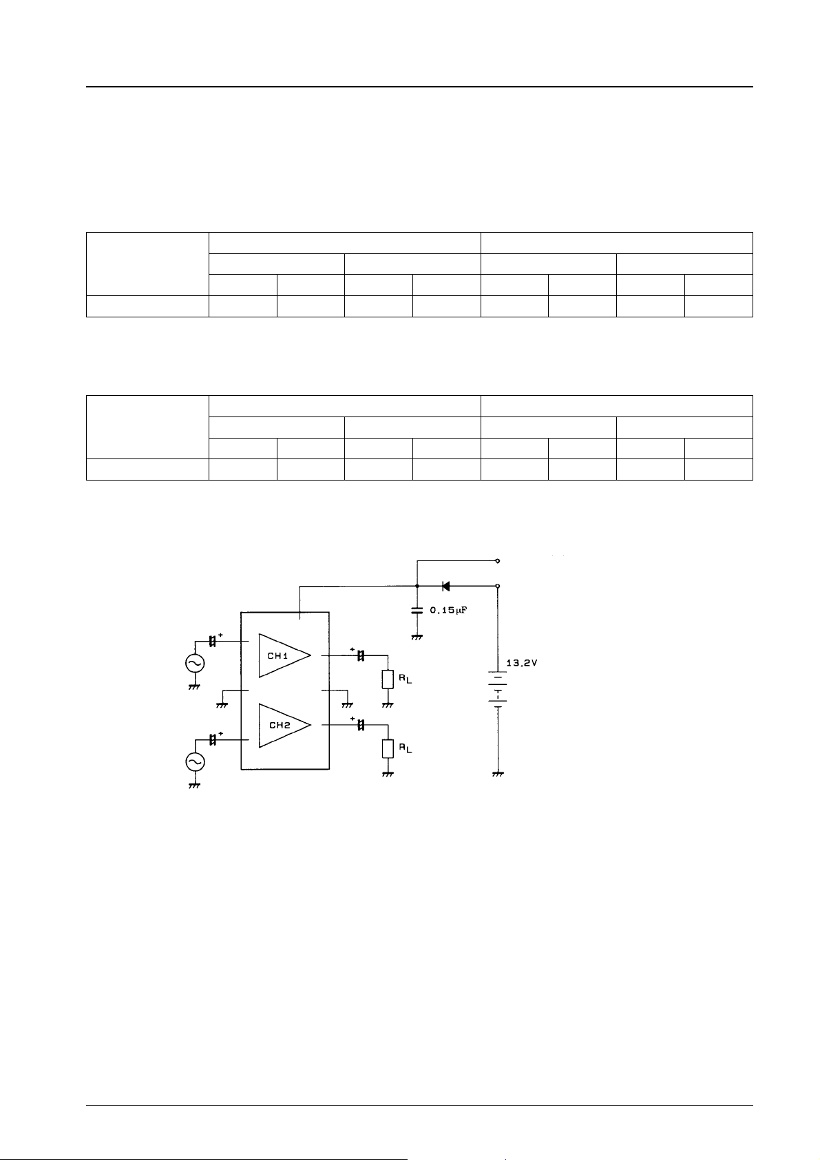
Dual-mode short-circuit
test circuit
1 Load short-circuit (to ground)
2 Output-to-supply short-circuit
3Output-to-ground short-ciruit
No.3680-17/20
Page 18

LA4485
.
Taking BTL coupling into consideration, the output-to-supply/output-to-ground protector is two-sided in order to protect both the
IC and the speaker.
Short-circuit to GND protection
Current × voltage
detector
Self-holding
positive feedback
circuit
CH1/CH2
Upper/lower
power transistor
control
Reset circuit
When using this method (simultaneously shorting the outputs to supply and to ground)
In BTL mode, the IC protection function works even in noninverted output → output-to-supply mode, inverted output →
output-to-ground mode. (The reverse is also OK.)
Reference Value
(a) Short-circuit test for dual-mode operation after the main and standby switches are turned ON.
Conditions: 1 V
2 V
3 V
=10to16V,RL=4Ωand PO= 1 to 5 W (variable) for load short-circuit
CC
=10to16V,RL=4Ω, Rg = 0 (no signal) for output-to-supply short-circuit
CC
=10to16V,RL=4Ω, Rg = 0 (no signal) for output-to-ground short-circuit.
CC
Z: impedance j: no device breakdown
1 Load short-circuit 2 Output-to-supply short-circuit 3 Output-to-ground short-circuit
One-time test Repeated switching test One-time test Repeated switching test
Z=0 Z=0.5Ω Z=0 Z=0.5Ω Z=0 Z=0.5Ω Z=0 Z=0.5Ω
j jjjjjjjj
(b) Short-circuit test for dual-mode operation (opposite flow of (a)) after the main and standby switches are turned ON.
Conditions: same as (a) j: No device breakdown
1 Load short-circuit 2 Output-to-supply short-circuit 3 Output-to-ground short-circuit
One-time test Repeated switching test One-time test Repeated switching test
Z=0 Z=0.5Ω Z=0 Z=0.5Ω Z=0 Z=0.5Ω Z=0 Z=0.5Ω
j jjjjjjjj
(Note) Shorting the outputs to ground when muting is active can result in device breakdown.
.
BTL-mode short-circuit test circuit
Noninverting
Inverting
1 Load short-circuit
2 Output-to-supply short-circuit
3 Output-to-ground short-circuit
No.3680-18/20
Page 19
LA4485
Reference Value
(a) Short-circuit test for BTL-mode operation after the main and standby switches are turned ON.
Conditions: 1 V
2 V
3 V
Z: impedance j: no device breakdown
1 Load short-circuit 2 Output-to-supply short-circuit 3 Output-to-ground short-circuit
j jjjjjjjj
(b) Short-circuit test for BTL-mode operation (opposite flow of (a)) after the main and standby switches are turned ON.
Conditions: same as (a) j: No device breakdown
1 Load short-circuit 2 Output-to-supply short-circuit 3 Output-to-ground short-circuit
j jjjjjjjj
=10to16V,RL=4Ωand PO= 1 to 15 W (variable) for load short-circuit
CC
=10to16V,RL=4Ω, Rg = 0 (no signal) for output-to-supply short-circuit
CC
=10to16V,RL=4Ω, Rg = 0 (no signal) for output-to-ground short-circuit.
CC
One-time test Repeated switching test One-time test Repeated switching test
Z=0 Z=0.5Ω Z=0 Z=0.5Ω Z=0 Z=0.5Ω Z=0 Z=0.5Ω
One-time test Repeated switching test One-time test Repeated switching test
Z=0 Z=0.5Ω Z=0 Z=0.5Ω Z=0 Z=0.5Ω Z=0 Z=0.5Ω
(Note) Shorting the outputs to ground when muting is active can result in device breakdown.
.
Power supply positive surge
JASO test
The power supply line positive surge breakdown margin has been increased by using the built-in overvoltage protection circuits
(V
= 28 V) to cut off all bias circuits/change the base-emitter reverse of the output stage. In other words, the breakdown
CCX
margin is being raised by changing output stage groups that operate as the V
CEO(VCER
) type to the V
CES(VCBO
) type.
No.3680-19/20
Page 20
LA4485
.
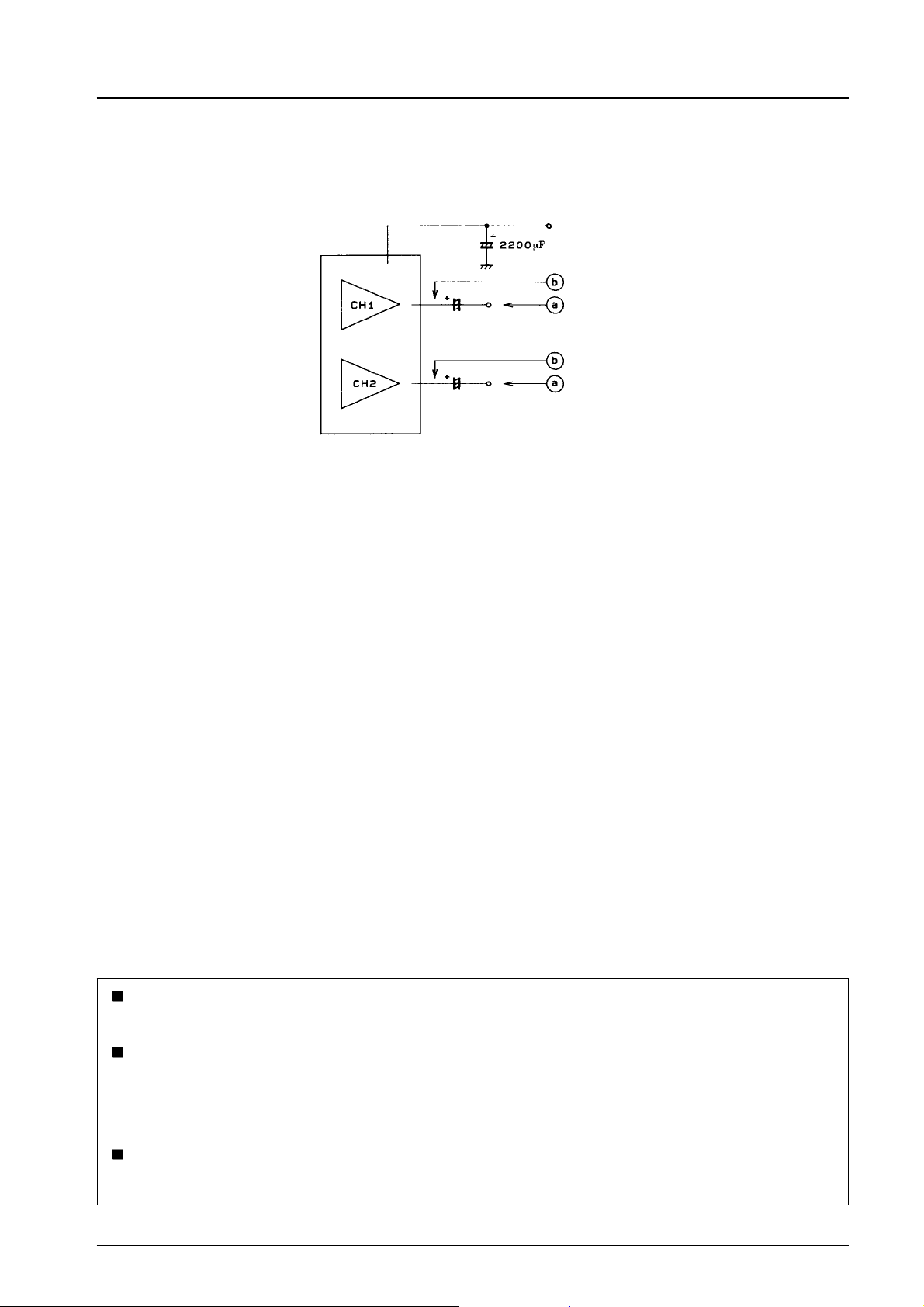
Test of application of +VCCto output pins
If the power supply pin is floating under the power supply capacitor insertion conditions, and +V
output lines (a) and (b) as shown in the diagram above, the IC’s internal upper power transistor will generally be damaged. The
LA4485 has a protective bypass circuit on chip. However, it is dangerous if the power supply capacitor is greater than 2200 µF.
Floating
comes into contact with
CC
No products described or contained herein are intended for use in surgical implants, life-support systems, aerospace equipment,
nuclear power control systems, vehicles, disaster/crime-prevention equipment and the like, the failure of which may directly or
indirectly cause injury, death or property loss.
Anyone purchasing any products described or contained herein for an above-mentioned use shall:
1 Accept full responsibility and indemnify and defend SANYO ELECTRIC CO., LTD., its affiliates, subsidiaries and distributors
and all their officers and employees, jointly and severally, against any and all claims and litigation and all damages, cost and
expenses associated with such use:
2 Not impose any responsibility for any fault or negligence which may be cited in any such claim or litigation on SANYO
ELECTRIC CO., LTD., its affiliates, subsidiaries and distributors or any of their officers and employees jointly or severally.
Information (including circuit diagrams and circuit parameters) herein is for example only; it is not guaranteed for volume
production. SANYO believes information herein is accurate and reliable, but no guarantees are made or implied regarding its use
or any infringements of intellectual property rights or other rights of third parties.
This catalog provides information as of July, 1996. Specifications and information herein are subject to change without notice.
No.3680-20/20
 Loading...