

Page 1
Ordering number: EN1321E
Monolithic Linear IC
LA4261
3.5 W 2-Channel AF Power Amplifier for
Home Stereos and Music Centers
Features
.
Minimum number of external parts required (No input
capacitor, bootstrap capacitor required).
.
High output: 3.5 W typ. ×2.
.
Soft clip, causing little harmonic disturbance to radios
(See page 8).
.
Small pop noise at the time of power switch ON/OFF
(See page 8).
.
Built-in protector against abnormal modes (Thermal
shutdown, overvoltage).
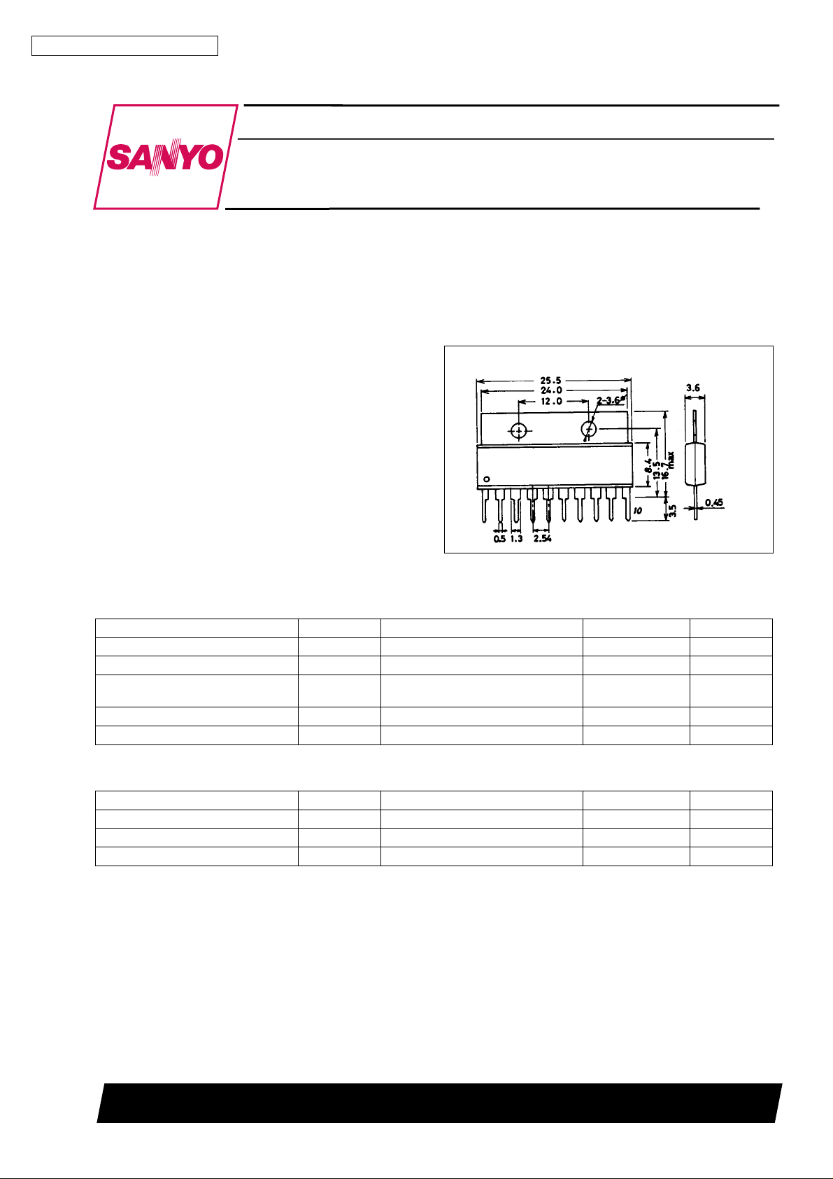
Package Dimensions
3018A-SIP10F
unit : mm
[LA4261]
SANYO : SIP10F
Specifications
Maximum Ratings at Ta = 25°C
Parameter Symbol Conditions Ratings Unit
Maximum supply voltage V
Maximum output current I
Allowable power dissipation Pd max
Operating temperature Topr –20 to +75 °C
Storage temperature Tstg –40 to +150 °C
max 25 V
CC
OP
1 channel 2.0 A
With heat sink
(see Pd – Ta characteristics)
7.5 W
Operating Conditions at Ta = 25°C
parameter Symbol Conditions Ratings Unit
Recommended supply voltage V
Recommended load resistance R
Operating supply voltage range V
CC
CC
L
op 9to24 V
16 V
8 Ω
SANYO Electric Co.,Ltd. Semiconductor Bussiness Headquarters
TOKYO OFFICE Tokyo Bldg., 1-10, 1 Chome, Ueno, Taito-ku, TOKYO, 110 JAPAN
22897HA(II)/71093TS/2126KI/8064KI/8053KI,MT No.1321-1/8
Page 2
LA4261
Operating Characteristics at Ta = 25°C, VCC=16V,RL=8Ω,f=1kHz, Rg = 600 Ω, (circuit 1)
Parameter Symbol Conditions min typ max Unit
Quiescent current I
CCO
Voltage gain VG 48 50 52 dB
Output power P
O
Total harmonic distortion THD P
Output noise voltage V
NO
THD = 10% 3.0 3.5 W
= 0.5 W 0.3 1.0 %
O
Rg=10kΩ, BW = 20 Hz to 20 kHz 0.65 1.5 mV
Ripple rejection ratio Rr Rg = 0, Vr = 500 mV 40 50 dB
Crosstalk CT Rg = 10 kΩ 40 55 dB
Voltage gain difference ∆VG 1.5 dB
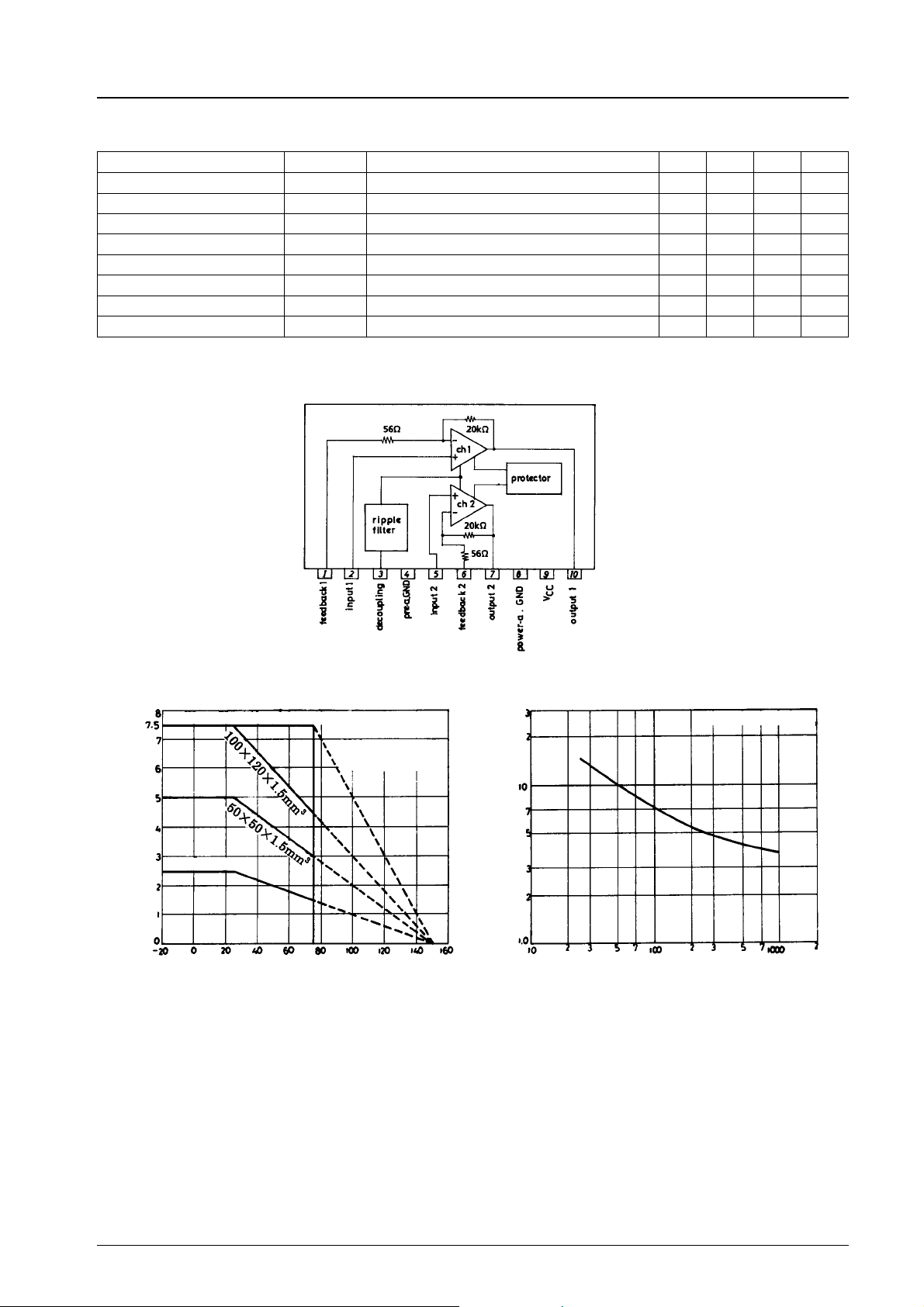
Equivalent Circuit Block Diagram
46 62 mA
Infinite heat sink
2.5 No heat sink
Allowable power dissipation, Pd max – W
Pd max – Ta
Al heat sink
Tightening torque 39 Nccm
Silicon grease applied
Thermal resistance
between junction and
outside air θj-c 10°C/W
Ambient temperature, Ta – °C
– °C/W
f
Thermal resistance of heat sink, θ
θf–S
f
Al heat sink t = 1.5 mm
Area of heat sink, Sf–cm
2
No.1321-2/8
Page 3
LA4261
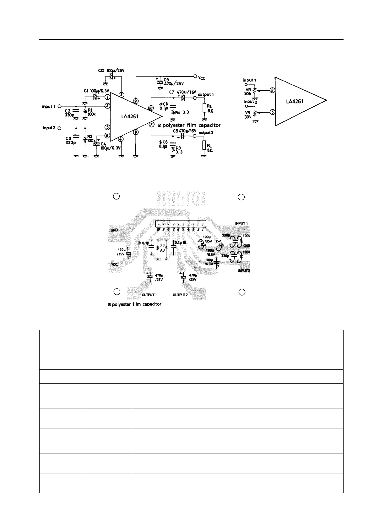
Sample Application Circuit 1:
Recommended Circuit
Sample Printed Circuit Pattern
Sample Application Circuit 2:
Circuit with minimum number of external
parts
Unit (resistance: Ω, capacitance: F)
Unit (resistance: Ω, capacitance: F)
Description of External Parts
C1, C4 100 µF Feedback capacitor
C2, C3 330 pF Input short capacitor
C5, C7 470 µF Output capacitor
C6, C8 0.1 µF
polyester film
capacitor
C9 470 µF Power capacitor
C10 100 µF Ripple filter capacitor
R1, R2 100 kΩ Input bias resistor
R3, R4 3.3 Ω Resistor connected in series with oscillation blocking capacitor.
Decreasing the capacitance value lowers the low frequency response. Increasing the
capacitance value makes the starting time later.
Reduces the high frequency noise when the input impedance is increased. Not required
when the input impedance is decreased.
Decreasing the capacitance value causes insufficient power at low frequencies.
Oscillation blocking capacitor
Decreasing the capacitance value causes oscillation to occur easily. Use a polyester film
capacitor that is good in high frequency response and temperature characteristic. The use
of an electrolytic capacitor may cause oscillation to occur at low temperatures.
Decreasing the capacitance value causes ripple to occur. Locating at a distance from the
IC or removing this capacitor may cause oscillation to occur.
Decreasing the capacitance value excessively or removing this capacitor causes ripple to
occur. However, increasing the capacitance value does not always cause ripple to be
reduced. Decreasing the capacitance value makes the starting time earlier.
Determines the bias (bias of GND potential) to be applied to the input pin and the input
impedance. Not required if variable resistors are used.
Prevents phase shift attributable to the oscillation blocking capacitor so that oscillation is
hard to occur.
No.1321-3/8
Page 4
Note for Changing Voltage Gain
LA4261
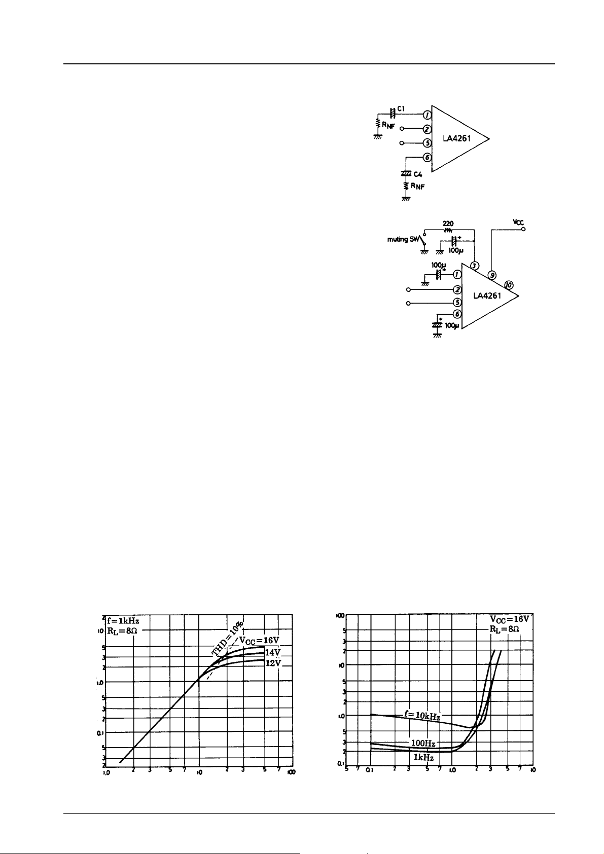
Basically, the voltage gain can be reduced by adding external
resistors (R
However, it should be noted that since there is no phase
compensation pin the frequency response is extended and
oscillation is liable to occur when the voltage gain is reduced.
The voltage gain must not be reduced to be less than 30 dB.
) in series with feedback capacitors C1, C4.
NF
External Muting
If external muting is required, make the circuit as shown right.
In this case, the attack time, recovery time, and pop noise are
similar to those which occur at the time of power switch
ON/OFF.
Unit (resistance: Ω, capacitance: F)
Proper Cares in Using IC
.
Maximum ratings
If the IC is used in the vicinity of the maximum ratings, even a slight variation in conditions may cause the maximum ratings to
be exceeded, thereby leading to breakdown. Allow an ample margin of variation for supply voltage, etc. and use the IC in the
range where the maximum ratings are not exceeded.
.
Pin-to-pin short
If power is applied when the space between pins is shorted, breakdown or deterioration may occur. When mounting the IC on
the board or applying power, make sure that the space between pins is not shorted with solder, etc.
.
When using in radios, allow a sufficient space between IC and bar antenna.
.
Printed circuit pattern
When designing the printed circuit pattern, make the power supply, output, and ground lines thick and short and arrange the
pattern and parts so that no feedback loop is formed between input and output. Place power capacitor C9, oscillation blocking
capacitors C6, C8 as close to IC pins as possible to prevent oscillation from occurring. Refer to the sample printed circuit
pattern.
–W
O
Output power, P
PO–V
IN
Input voltage, VIN–mV
THD–P
Total harmonic distortion, THD – %
Output power, PO–W
O
No.1321-4/8
Page 5
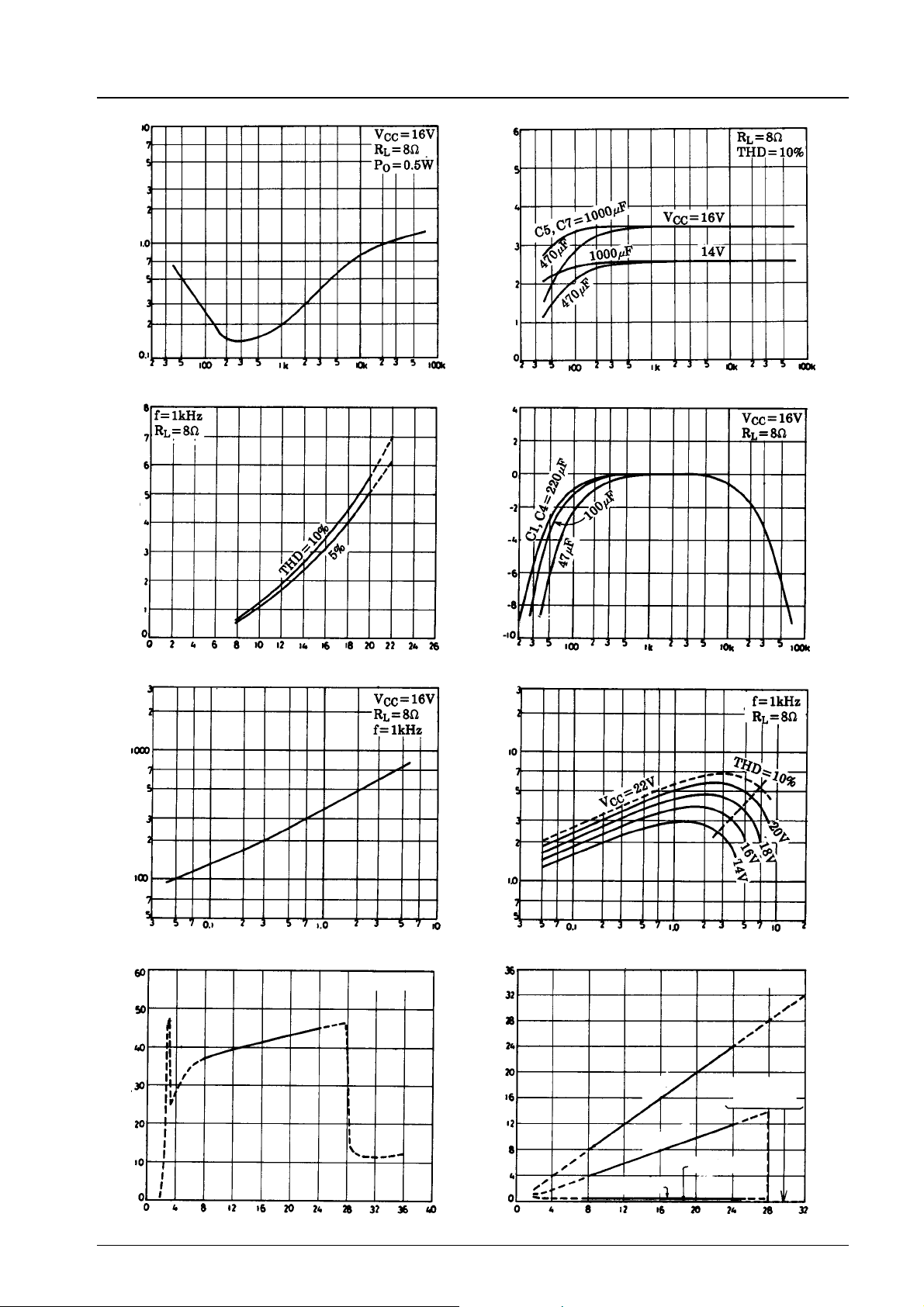
LA4261
Total harmonic distortion, THD – %
–W
O
Output power, P
THD–f
Frequency,f–Hz
PO–V
CC
–W
O
Output power, P
Response – dB
–f
P
O
Frequency,f–Hz
f Response
–mA
CC
Current dissipation, I
–mA
CCO
Supply voltage, VCC–V
ICC–P
O
Output power, PO–W
I
CCO–VCC
Quiescent
Power dissipation, Pd – W
Frequency,f–Hz
Pd–P
O
Output power, PO–W
Vpin – V
Pin 3
CC
Pin 1, 2, 4,
Quiescent
6, 7, 10
Pin voltage, Vpin – V
Quiescent current, I
Pin 7, 10
Pin 2, 4
Pin 1, 6
Supply voltage, V
CC
–V
Supply voltage (pin 9), V
CC
–V
No.1321-5/8
Page 6
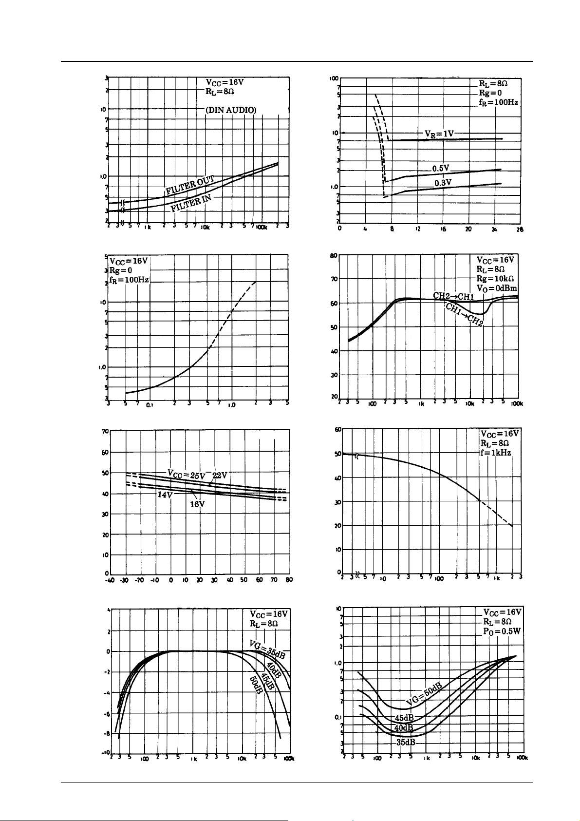
LA4261
–mV
Output noise voltage, V
NO
VNO–Rg
FILTER 20 Hz to 20 kHz
Signal source resistance, Rg – Ω
Vro–Vr
Vro–V
CC
Output ripple voltage, Vro – mV
Supply voltage, VCC–V
CT–f
Output ripple voltage, Vro – mV
–mA
CCO
Quiescent current, I
Ripple voltage, Vr – V
I
–Ta
CCO
Ambient temperature, Ta – °C
f Response
Quiescent
Crosstalk, CT – dB
Frequency,f–Hz
VG–R
NF
Voltage gain, VG – dB
External resistance, RNF– Ω
THD–f
Response – dB
Total harmonic distortion, THD – %
Frequency,f–Hz
Frequency,f–Hz
No.1321-6/8
Page 7
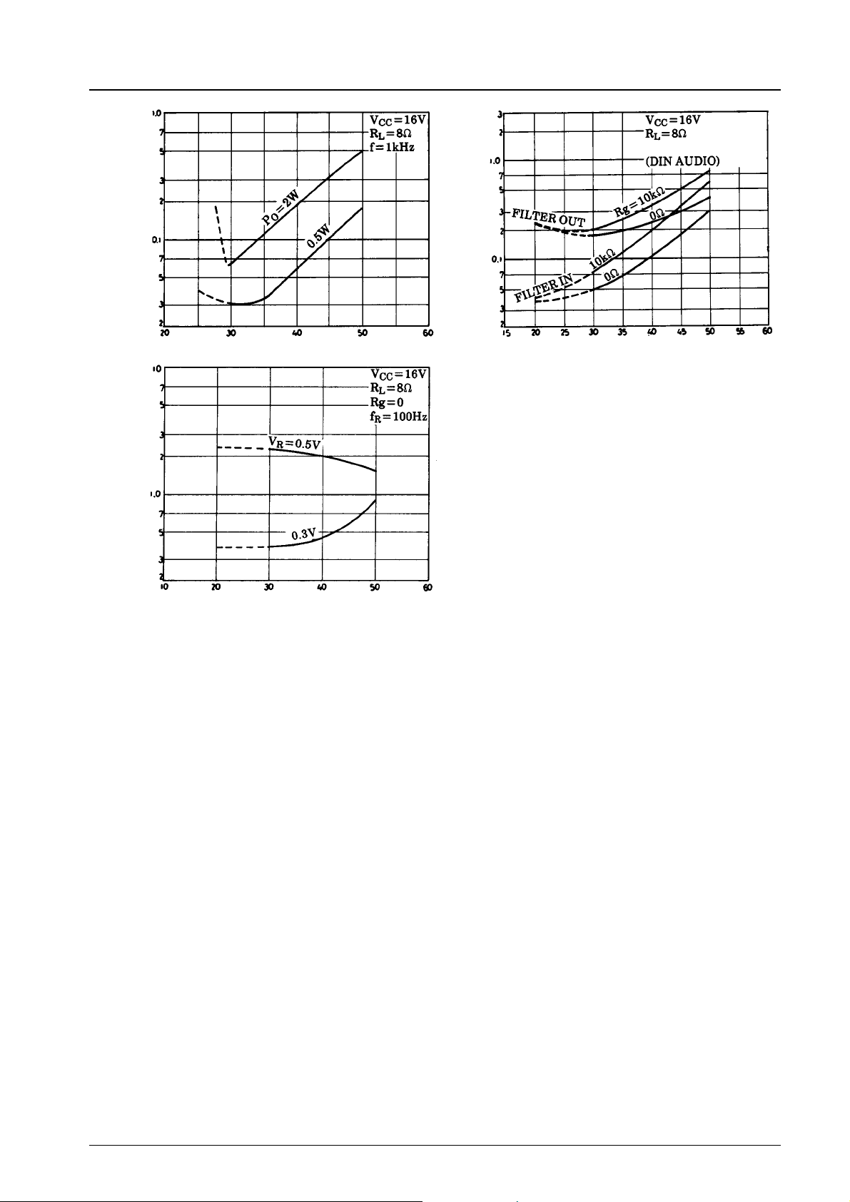
LA4261
THD–VG
–mV
NO
Total harmonic distortion, THD – %
Voltage gain, VG – dB
Output noise voltage, V
Voltage gain, VG – dB
–VG
V
NO
FILTER 20 Hz to 20 kHz
Vrp–VG
Output ripple voltage, Vrp – mV
Voltage gain, VG – dB
No.1321-7/8
Page 8
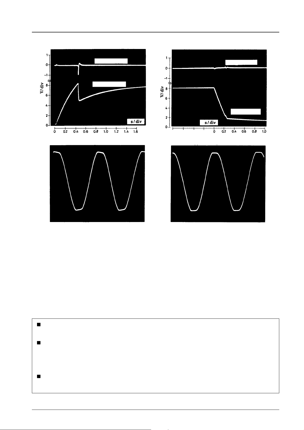
LA4261
Pop Noise Waveform at The Time of Power Switch ON
(VCC=16V,RL=8Ω, quiescent)
Pop noise waveform
Middle point rise
waveform
f = 1 kHz Clip waveform
(VCC=16V,RL=8Ω, THD = 5%)
Pop Noise Waveform at The Time of Power Switch OFF
(VCC=16V,RL=8Ω, quiescent)
Pop noise waveform
Middle point fall
waveform
f = 10 kHz Clip waveform
(VCC=16V,RL=8Ω, THD = 5%)
No products described or contained herein are intended for use in surgical implants, life-support systems, aerospace equipment,
nuclear power control systems, vehicles, disaster/crime-prevention equipment and the like, the failure of which may directly or
indirectly cause injury, death or property loss.
Anyone purchasing any products described or contained herein for an above-mentioned use shall:
1 Accept full responsibility and indemnify and defend SANYO ELECTRIC CO., LTD., its affiliates, subsidiaries and distributors
and all their officers and employees, jointly and severally, against any and all claims and litigation and all damages, cost and
expenses associated with such use:
2 Not impose any responsibility for any fault or negligence which may be cited in any such claim or litigation on SANYO
ELECTRIC CO., LTD., its affiliates, subsidiaries and distributors or any of their officers and employees jointly or severally.
Information (including circuit diagrams and circuit parameters) herein is for example only; it is not guaranteed for volume
production. SANYO believes information herein is accurate and reliable, but no guarantees are made or implied regarding its use
or any infringements of intellectual property rights or other rights of third parties.
This catalog provides information as of February 1997. Specifications and information herein are subject to change without notice.
No.1321-8/8
 Loading...