

Page 1

Ordering number: EN887B
Monolithic Linear IC
LA4183
2.3 W 2-Channel AF Power Amplifier for Radio
Cassette Players
Features
.
Built-in 2 channels enabling use in stereo and bridge
amplifier (BTL) applications.
.
High-output:
2.3 W typ./channel, V
4.7 W typ./bridge amplifier, V
.
Low switching distortion at high frequencies.
.
Minimum number of external parts required: 9 pcs. min.
(Stereo/bridge).
.
Small shock noise at the time of power supply ON/OFF due
to built-in muting circuit.
.
Good ripple rejection due to built-in ripple filter.
.
Soft tone at the time of output saturation.
.
Good channel separation.
.
Voltage gain fixed at 45 dB (Bridge: 51 dB).
Variable voltage gain available with external resistor added.
=9V,RL=4Ω
CC
=9V,RL=8Ω
CC
Package Dimensions
unit : mm
3022A-DIP12F
[LA4183]
SANYO : DIP12F
Note:
In general applications, heat generated in the DIP 12-pin
package can be radiated through the Cu-foiled area of the
printed circuit board, but since power dissipation Pd may be
increased depending on the supply voltage and load conditions,
it is recommended to use a fin additionally.
Specifications
Maximum Ratings at Ta = 25°C
Parameter Symbol Conditions Ratings Unit
Maximum supply voltage V
Allowable power dissipation Pd max
Operating temperature Topr –20 to +75 °C
Storage temperature Tstg –55 to +150 °C
CC
max
With signal 11 V
Quiescent 15 V
With printed circuit board
(Refer to Pd – Ta characteristics)
4W
Operating Conditions at Ta = 25°C
Parameter Symbol Conditions Ratings Unit
Recommended supply voltage V
Load resistance R
CC
L
Stereo 4.0 to 8.0 Ω
Bridge 8.0 Ω
9.0 V
SANYO Electric Co.,Ltd. Semiconductor Bussiness Headquarters
TOKYO OFFICE Tokyo Bldg., 1-10, 1 Chome, Ueno, Taito-ku, TOKYO, 110 JAPAN
53096HA(II)/O0207TA/2022KI,TS,ID No.887-1/11
Page 2

LA4183
Operating Characteristics at Ta = 25°C, VCC=9.0V,f=1kHz, Rg = 600 Ω,RL=4Ω, ( ): 8 Ω,
See specified Test Circuit.
Parameter Symbol Conditions min typ max Unit
Quiescent current I
CCO
Voltage gain VG Closed loop, V
Voltage gain difference ∆VG Stereo ±1dB
Output power P
Total harmonic distortion THD P
Input resistance ri 21 30 kΩ
Output noise voltage V
NO
Ripple rejection ratio — Rg = 0, Vr = 150 mV Stereo 40 46 dB
Channel separation CHsep Rg = 10 kΩ,V
Pd max – Ta
Cu plate (fin1)
Fe plate (fin 1)
For stereo 40 55 mA
Stereo 43 45 47 dB
Bridge 49 51 53 dB
Stereo
1.7 2.3 W
(1.3) W
O
THD = 10%
= –45 dB
IN
Bridge (4.7) W
= 250 mW
O
Stereo 0.3 1.5 %
Bridge 0.5 %
Rg = 0 Stereo 0.3 1.0 mV
Rg=10kΩ Stereo 0.5 2.0 mV
= 0 dBm Stereo 40 55 dB
O
Fe plate (fin 2)
Recommended
printed circuit
board only
Cu-foiled area
reduced board
IC only
Allowable power dissipation, Pd max – W
Ambient temperature, Ta – °C
Pin Assignment and Equivalent Circuit
No.887-2/11
Page 3

LA4183
Sample Application Circuit 1: Stereo amplifier
Sample Application Circuit 2: Bridge amplifier
Example of printed circuit pattern
(Cu-foiled area) for use in stereo, bridge amplifier applications
60 × 80 mm
2
C3
100µF
/16V
C1
100µF/16V
C2
100µF/16V
BTL use
IN1
100µF
/16V
IN2
BTL OUT
C9
100µF/16V
7
LA4183
6
12
GND
1
C4
100µF/16V
C7
OUT1
470µF
/16V
V
CC
C5
0.15µF
jumper
2ch stereo use
C6
0.15µF
OUT2
C8
470µF/16V
C10
1000µF
/16V
No.887-3/11
Page 4

Description of External Parts
LA4183
C1 (C2) Feedback capacitor The low-range cut-offfrequency is determined by the following formula:
C3 (C4) Bootstrap capacitor The output at low frequencies depends on this capacitor. Ifthe capacity
C5 (C6) Oscillation preventing capacitor Use polyesterfilm capacitor whichis good in temperature characteristic
C7 (C8) Output capacitor The low-range cut-off frequency is determinedby the following formula.
C9 Decoupling capacitor Used for the ripple filter. Since the rejection effect is saturated at a
C10 Power source capacitor
f
=1/(2πC1vRf), fL: Low-range cut-off frequency
L
The frequency, however, affects the starting time in conjuction with
decoupling capacitors. Therefore, it is necessary to determine it after a
full review of the required low-frequency range and other similar
conditions.
is decreased, the output at low frequencies goes lower. 47 µF min. is
required.
and frequency characteristic. Aluminum electrolytic capacitor or
ceramic capacitor causes oscillation at low temperatures.
f
=1/(2πC7vRL), fL: Low-range cut-off frequency
L
When using bridge-connected, double the capacitance to obtain
equivalent low-range frequency characteristics to those in a 2-channel
application.
certain capacity, it is meaningless to increase the capacity more than
needed.
This capacitor, being also used for the time constant of the muting
circuit, affects the starting time.
Rf: Feedback resistor
(50 Ω embedded + Rf externally connected)
R
:Load resistance
L
Application Circuits
1. Voltage gain adjustment
.
Stereo
The voltage gain depends on built-in-resistors R1 (R2), R3 (R4) as follows:
VG = 20 log
If the IC is used at a voltage gain less than this, the following
equation with Rf added applies.
VG = 20 log
where R1 (R2) = 50 Ω typ.,
R3 (R4) = 10 kΩ typ.
.
Bridge
The following shows the bridge amplifier configuration, where ch1 operates as a non-inverting amplifier and ch2 as an inverting
amplifier.
R3 (R4)
R1 (R2)
[dB]
R3 (R4)
R1 (R2) + Rf
[dB]
No.887-4/11
Page 5
LA4183
The output of ch1 is divided with R5, R6 and led to pin 1 and then inputted to ch2. Since the attenuation degree (R5/R6) of ch1
output and the amplification degree (R4/R2 + R6)) of ch2 are fixed at an equal value, the ch2 output is in opposite phase with the
ch1 output. Therefore, the total voltage gain gets apparently 6 dB higher than the voltage gain of ch1 alone and is determined by
the following equation.
VG = 20 log
If the IC is used at a voltage gain less than this, the following equation with Rf added applies.
VG = 20 log
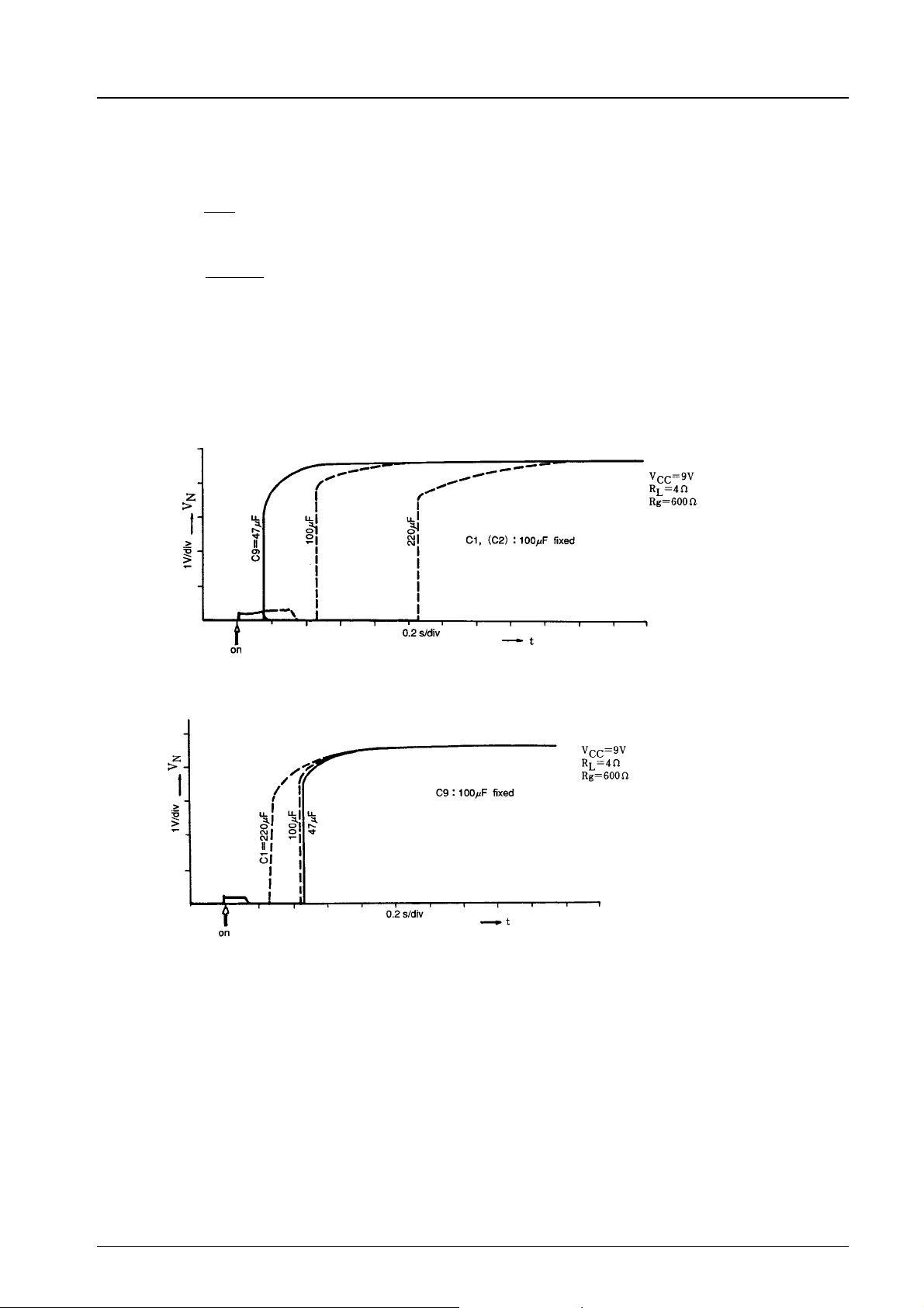
2. Starting time
Starting time depends on capacitance of C1 (C2) and C9 as shown in the diagram below. That is because of using a muting circuit
utilizing the C9 (decoupling capacitor) time constant for pop noise prevention when power is turned on and charging circuits for
C1 and C2 (NF capacitors).
R3
+ 6 [dB]
R1
R3
R1+Rf
+ 6 [dB]
Quiescent
Dependence on C9
Quiescent
Dependence on C1 (C2)
3. Crosstalk
Channel separation characteristic is important for single-package IC embodying two channels.
With LA4183, good channel separation is obtainable even as is, but if the BTL OUT pin (pin 1) is not grounded, it will invite
imbalance in crosstalk between the two channels. (Refer to the characteristics diagram.)
No.887-5/11
Page 6
LA4183
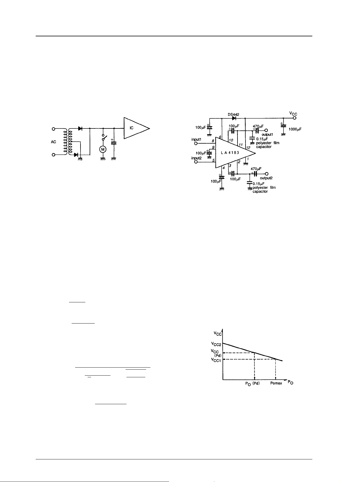
Proper Cares in Operating a Set with LA4183 Incorporated
When a set with the LA4183 incorporated is operated from AC power supply, a momentary drop in supply voltage is caused by
the transformer regulation, etc. at the time of turning ON the motor with the circuit shown below. In this case, if ripple noise is
generated from the speaker or headphone, take the following actions.
1. Connect a diode (rectifier diode of average rectified current I
the voltage at pin 6 can follow the supply voltage regulation. In the steady state, this diode is cut off.
2. Increase the capacity of the power source capacitor so that the supply voltage regulation can be minimized.
= 100 to 200 mA) across pins 6 and 12 of the LA4183 so that
O
Radiation Design
.
Since the DIP 12-pin package is so designed as to be able to radiate heat through the Cu-foiled area of printed circuit board
under normal operating conditions, make the Cu-foiled area near the fin of IC as large as possible when designing the printed
circuit board.
.
By providing the Cu-foiled area covered by the broken line as shown in the above-mentioned example of printed circuit pattern,
a rather satisfactory radiation is enabled. (Refer to the Pd − Ta characteristics.)
.
Since the power dissipation (Pd) goes higher depending on the conditions of supply voltage and load, it is recommended to use
the fin together with the printed circuit board.
.
The following equations are rule-of-thumb guides for Pd (for stereo). For AC power supply, it is desirable to measure with the
transformer of each individual set. In the bridge amplifier application, calculation should be made with 1/2 of the load used.
(1) DC Power supply
2
V
CC
+I
v VCC(For stereo)
Pd max =
(2) AC power supply
Pd max =
V
CC2
I
CCO
V
CC
V
CC
V
CC
r: Voltage regulation,
.
Example of fin mounting
The fin is formed into such a shape as to be able to radiate heat from the plastic area of IC and the fin as shown below and is
soldered to the printed circuit board. For the fin size, refer to the Pd – Ta characteristics. The desirable material is copper or
iron which is solderable. It is recommended to apply silicone grease, etc. to the plastic area of IC in order to minimize the
thermal resistance.
π2R
V
: Quiescent supply voltage
: Quiescent current
(Pd): Supply voltage at Pd max. output,
(Pd) =
1+
1: Supply voltage at max. output
L
(Pd)
CC
π2R
L
√2 v π v R
CCO
2
rvV
V
+I
v VCC(Pd) (For stereo)
CCO
(1+r)V
CC1
×
L
CC2–VCC1
V
CC1
CC1
√
R
L
POmax
No.887-6/11
Page 7

LA4183
Printed circuit board
Example of fin mounting
Fin
IC Usage Notes
1. If the IC is used in the vicinity of the maximum rating, even a slight variation in conditions may cause the maximum rating
to be exceeded, thereby leading to a breakdown. Allow an ample margin of variation for supply voltage, etc. and use the IC
in the range where the maximum rating is not exceeded.
2. Pin-to-pin short
If the supply voltage is applied when the space between pins is shorted, a breakdown or deterioration may occur. When
installing the IC on the board or applying the supply voltage, make sure that the space between pins is not shorted with
solder, etc.
3. Load short
If the IC is used with the load shorted for a long time, a breakdown or deterioration will occur. Be sure not to short the load.
4. When the IC is used in radios or radio cassette tape recorders, keep a good distance between IC and bar antenna.
5. When making the board, refer to the example of printed circuit pattern.
No.887-7/11
Page 8
LA4183
–W
O
Output power, P
PO– V
IN
Input voltage, VIN–mV
THD–P
O
f response
Response – dB
Frequency,f–Hz
THD–f
Total harmonic distortion, THD – %
Output power, PO–W
THD–f
Total harmonic distortion, THD – %
Frequency,f–Hz
CHsep – f
Total harmonic distortion, THD – %
Frequency,f–Hz
VNO, THD, fH–VG
–mV
NO
VNO(Rg = 0.20 to 20kHz BPF)
Output noise voltage, V
Total harmonic distortion, THD – %
VNO(Rg = 0, no filter)
(With signal)
(With noise)
– kHz
H
High cutoff frequency, f
Voltage gain, VG – dB
Vrp,VNO–Rg
–mV
NO
Channel Separation, CHsep – dB
(Signal side)
Frequency,f–Hz
Output ripple voltage, Vrp – mV
Output noise voltage, V
Signal source resistance, Rg – Ω
No.887-8/11
Page 9
LA4183
THD–Rg
ripple
Total harmonic distortion, THD – %
Signal source resistance, Rg – Ω
Vrp–C
NF
No difference due to
bootstrap capacitors
47 µF, 100 µF, 200 µF.
Output ripple voltage, Vrp – mV
Decoupling capacitor capacity, CDC–µF
Vrp–C
Vrp–fr
DC
Output ripple voltage, Vrp – mV
Feedback capacitor capacity, C
VG–R
NF
Voltage gain, VG – dB
External feedback resistor resistance, RNF– Ω
t
S–CDC
Output DC waveform
Power ON
–s
s
–µF
NF
Measured value
Output ripple voltage, Vrp – mV
Total harmonic distortion, THD – %
Using specified fin
Ripplie frequency, fr – Hz
THD–V
CC
Supply voltage, VCC–V
Pd–P
O
Starting time, t
Power dissipation, Pd (Stereo) – W
Decoupling capacitor capacity, CDC–µF
Output power, PO–W
No.887-9/11
Page 10
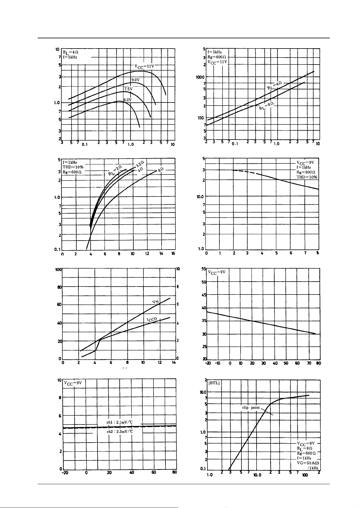
LA4183
Using specified fin
Power dissipation, Pd (Stereo) – W
–W
O
Pd–P
O
Output power, PO–W
PO–V
CC
–mA
CC
Current drain, I
–W
O
ICC–P
O
Output power, PO–W
P
O–RL
Output power, P
– mA (Stereo)
CCO
Quiescent current, I
–V
N
Supply voltage, VCC–V
I
CCO,VN–VCC
Supply voltage, VCC–V
VN–Ta
Output power, P
–V
N
– mA (Stereo)
CCO
Output midpoint voltage, V
Quiescent current, I
[Bridge]
–W
O
Load resistance, RL– Ω
I
–Ta
CCO
Ambient temperature, Ta – °C
P
O–VIN
Output power, P
Output midpoint voltage, V
Ambient temperature, Ta – °C
Input voltage, VIN–mV
No.887-10/11
Page 11
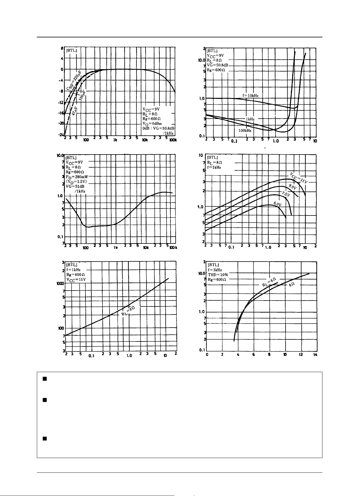
LA4183
f response
THD–P
O
Response – dB
Total harmonic distortion, THD – %
Frequency,f–Hz
THD–f
Using specified fin
Output power, PO–W
Pd–P
O
Power dissipation, Pd – W
Total harmonic distortion, THD – %
Frequency,f–Hz
ICC–P
O
–mA
CC
Current drain, I
–W
O
Output power, P
Output power, PO–W
No products described or contained herein are intended for use in surgical implants, life-support systems, aerospace equipment,
nuclear power control systems, vehicles, disaster/crime-prevention equipment and the like, the failure of which may directly or
indirectly cause injury, death or property loss.
Anyone purchasing any products described or contained herein for an above-mentioned use shall:
1 Accept full responsibility and indemnify and defend SANYO ELECTRIC CO., LTD., its affiliates, subsidiaries and distributors
and all their officers and employees, jointly and severally, against any and all claims and litigation and all damages, cost and
expenses associated with such use:
2 Not impose any responsibility for any fault or negligence which may be cited in any such claim or litigation on SANYO
ELECTRIC CO., LTD., its affiliates, subsidiaries and distributors or any of their officers and employees jointly or severally.
Information (including circuit diagrams and circuit parameters) herein is for example only; it is not guaranteed for volume
production. SANYO believes information herein is accurate and reliable, but no guarantees are made or implied regarding its use
or any infringements of intellectual property rights or other rights of third parties.
Output power, PO–W
PO–V
CC
Supply voltage, VCC–V
This catalog provides information as of May, 1996. Specifications and information herein are subject to change without notice.
No.887-11/11
 Loading...