

Page 1
Ordering number: EN 2651B
Monolithic Linear IC
LA3246
Stereo Preamplifier for Compact Double Cassette
Playback-only Use
Overview
The LA3246 is a stereo preamplifier IC for double cassette
tape playback-only use. The LA3246 is intended for use in
portable radio-cassette tape recorders and tape decks.
Applications
.
Stereo compact cassette player for playback-only use
.
Stereo cassette deck player
Functions
.
Preamplifier × 2, Mixing amplifier × 1, Electronic switch × 6
Features
.
On-chip electronic switch for input select (auto reverse or
A deck/B deck select)
.
On-chip electronic switch for normal/higher dubbing select
and electronic switch for metal/normal tape select
.
Wide operating voltage range (VCCop = 3.5 to 14 V)
.
With output MIX pin (for music select control)
.
Low noise voltage range (VNI= 0.9 µV typ, Rg = 2.2 kΩ
NAB)
.
Can be used in conjunction with the LA3240, 3241, 3242 to
easily make up a doublecassette dubbing system.
Package Dimensions
unit : mm
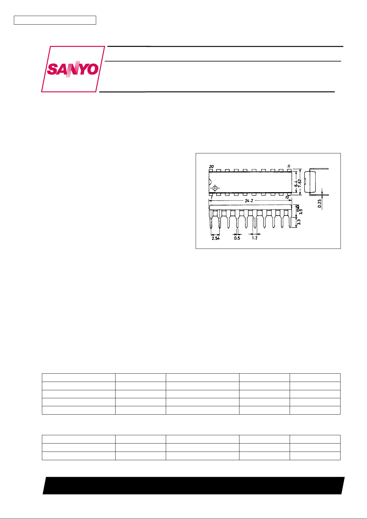
3021B-DIP20
[LA3246]
SANYO : DIP20 (300 mil)
Specifications
Maximum Ratings at Ta = 25°C
Parameter Symbol Conditions Ratings Unit
Maximum supply voltage V
Allowable power dissipation Pd max 500 mW
Operating temperature Topr –20 to +75 °C
Storage temperature Tstg –40 to +125 °C
Maxiumum Ratings at Ta = 25°C
Parameter Symbol Conditions Ratings Unit
Recommended supply voltage V
Operating voltage range V
max 16 V
CC
CC
op 3.5 to14 V
CC
6V
SANYO Electric Co.,Ltd. Semiconductor Bussiness Headquarters
TOKYO OFFICE Tokyo Bldg., 1-10, 1 Chome, Ueno, Taito-ku, TOKYO, 110 JAPAN
D3097HA(II)/41594HK/N107TA, TS No.2651-1/13
Page 2
LA3246
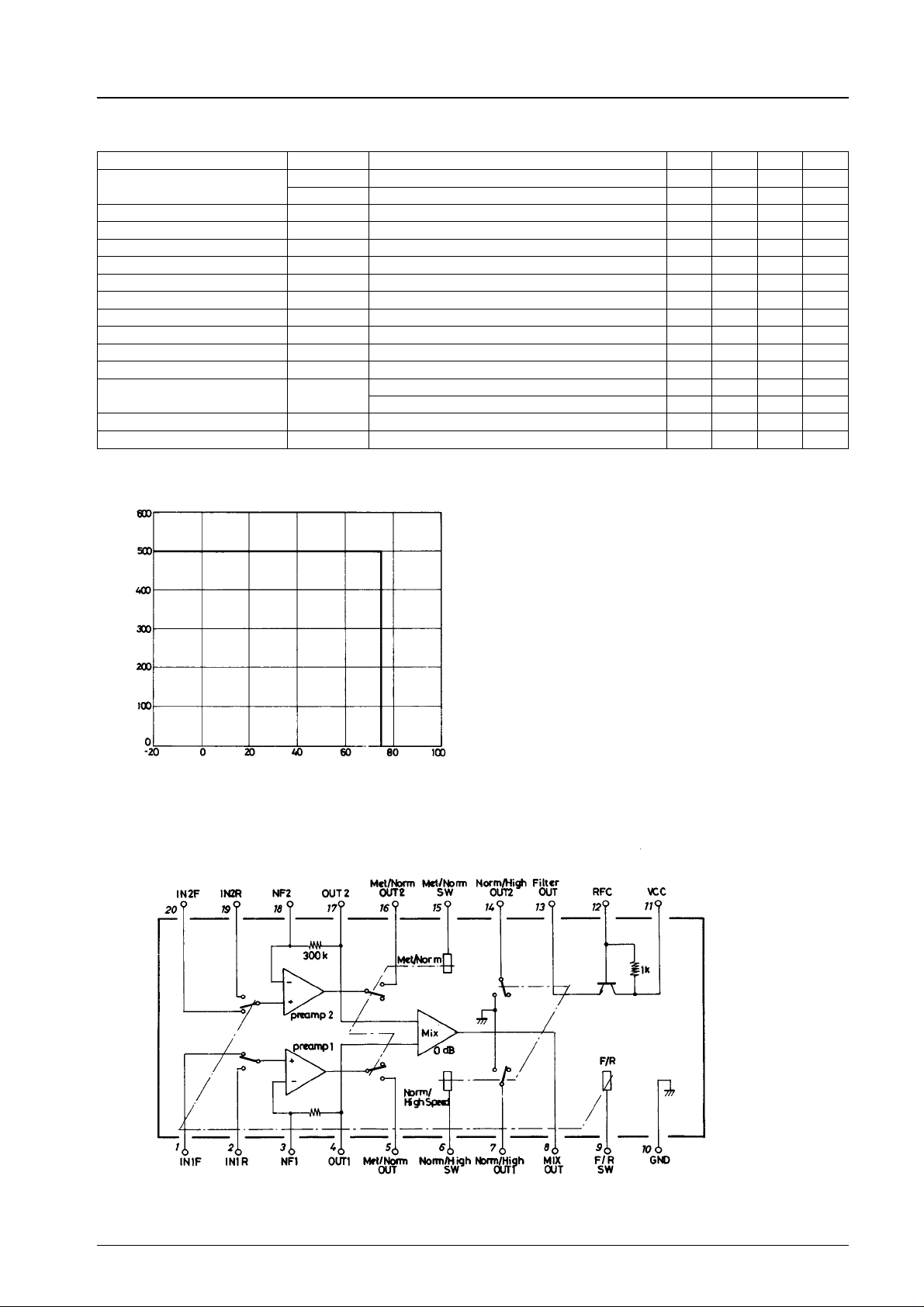
Operating Characteristics at Ta = 25°C, VCC= 6.0 V, RL=10kΩ,f=1kHz, 0 dB = 0.775 V
Parameter Symbol Conditions min typ max Unit
Quiescent current
Voltage gain (Open) VGo 75 85 dB
Voltage gain (Closed) VG Nor/Nor speed, NAB 39.5 40.5 41.5 dB
Total harmonic distortion THD V
Maximum output voltage V
Crosstalk (between channels) CT1 V
Crosstalk (between F/R) CT2 V
Channel balance V
Equivalent input noise voltage V
MIX output voltage V
Ripple filter output current I
Electronic switch ON-state
resistance
DC feedback resistance R
Input bias current I
Pd max – Ta
Icco Nor/Nor speed forward 5 7 12 mA
Iccs Metal/High speed forward 7 10 17 mA
= 0.65 V, Nor/Nor speed 0.03 0.2 %
max THD = 1%, Nor/Nor speed 0.7 1.2 V
O
BL
NI
MIX VO1, VO2 = 0 dBm –3 0 +3dB
O
F OUT
Ron
F
F
O
= –5 dBm, Rg = 2.2 kΩ, Nor/Nor speed 50 65 dB
O
= –5 dBm, Rg = 2.2 kΩ, Nor/Nor speed 50 65 dB
O
VIN= –50 dBm 0 2 dB
Rg = 2.2 kΩ, B.P.F 20 Hz to 20 kHz, Nor/Nor speed 0.9 1.7 µV
10 15 mA
Between P1 to P4 and 5, between pin 16 and 17 100 250 Ω
Between P1 to P7 and 10, between pin 10 and 14 30 70 Ω
240 300 360 Ω
0.5 3.0 µA
Allowable power dissipation, Pd max – mW
Ambient temperature, Ta – °C
Equivalent Circuit Block Diagram
Top view
No.2651-2/13
Page 3
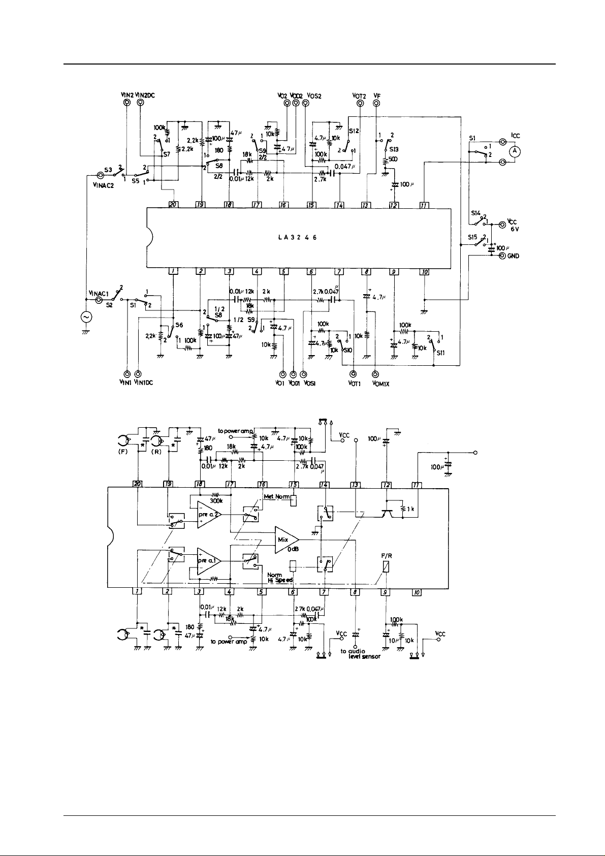
Test Circuit
LA3246
Sample Application Circuit
Unit (resistance: Ω, capacitance: F)
Note 1. The output frequency characteristic for Nor Tape/High speed mode (pin 6: High, pin 15: Low) and that for Metal
Tape/Nor speed mode (pin 6: Low, pin 15: Low) are set to be the same.
2. Since the input bias current flows out of pins 1, 2 and pins 19, 20, a resistor (recommended value: 30 kΩ to 350 kΩ,
maximum value: 500 kΩ) must be connected a coupling capacitor in series with these pins.
3. *: A capacitor must be connected to the input to absorb a surge.
4. The electronic select switching level is approximately 1/2 × (V
5. The value of the capacitor connected to pin 12 can be increased/decreased to adjust starting time t
application of V
worse.
6. No capacitor is connected to pin 13. (Even if connected, the ripple can not be rejected.)
7. Extreme caution should be exercised when handling the IC as it is subject to dielectric breakdown.
.(C=100µF,ts= 0.4 s.) If the capacitor value is made less than 47 µF, the ripple rejection will get
CC
CC
–0.9).
at the time of
s
No.2651-3/13
Page 4
LA3246
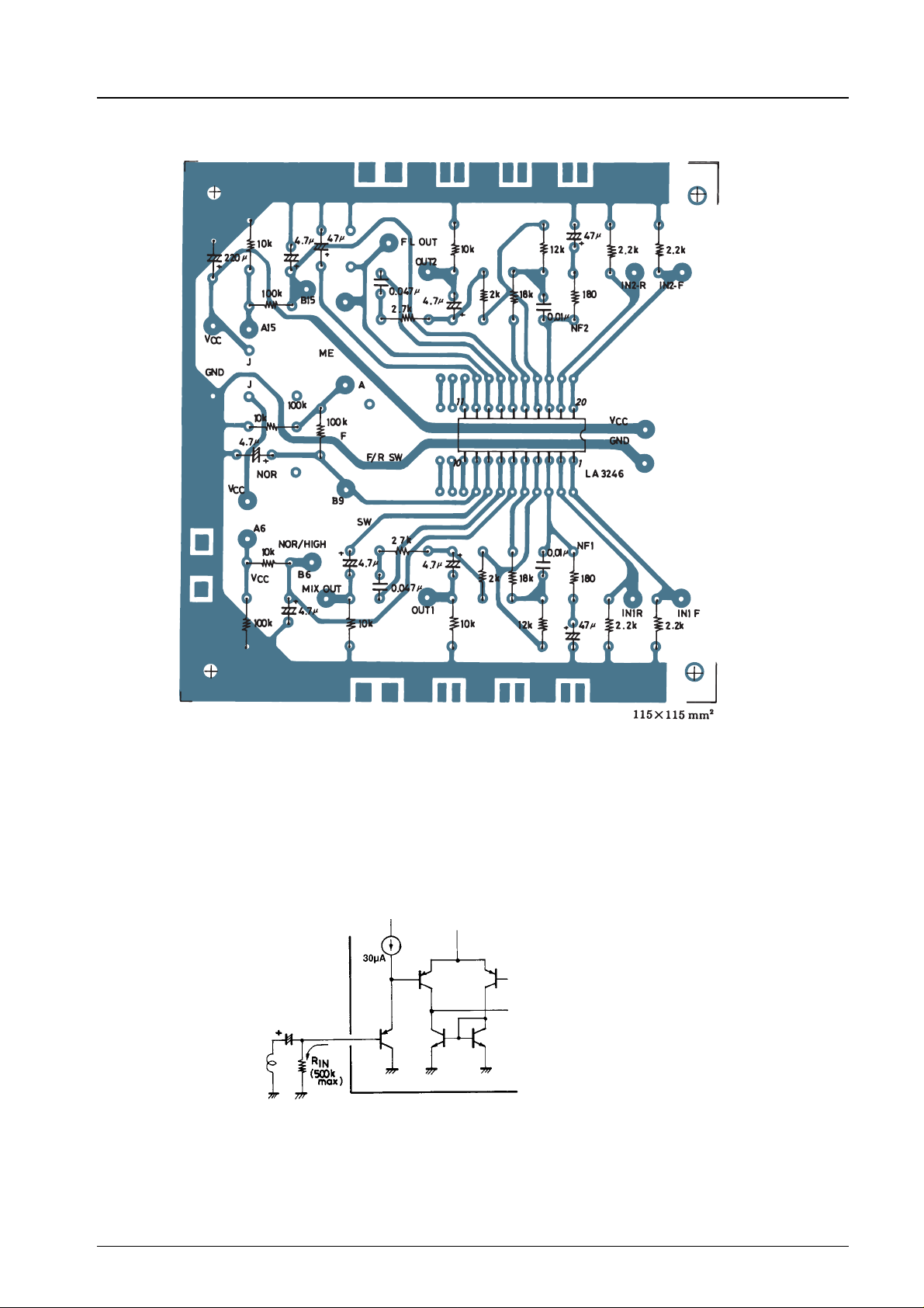
Sample Printed Circuit Pattern (Cu-foiled area)
Unit (resistance: Ω, capacitance: F)
IC Usage Notes
(1) It is recommended to connect a surge absorbing capacitor across input pins 1, 2 and GND and across input pins 19, 20 and
GND.
(2) The base of a PNP transistor is connected to input pins 1, 2 and 19, 20. If an electrolytic capacitor is connected in series with
the input pins, connect input resistor R
at the time of input switching)
If a resistor of more than 500 kΩ is connected across input pin and GND, the noise (output) caused by amp 1 and amp 2 select is
liable to increase at the time of F/R switching.
must not exceed 500 kΩ. (Reason: To minimize the variation in output DC voltage
IN
Ω
No.2651-4/13
Page 5
LA3246
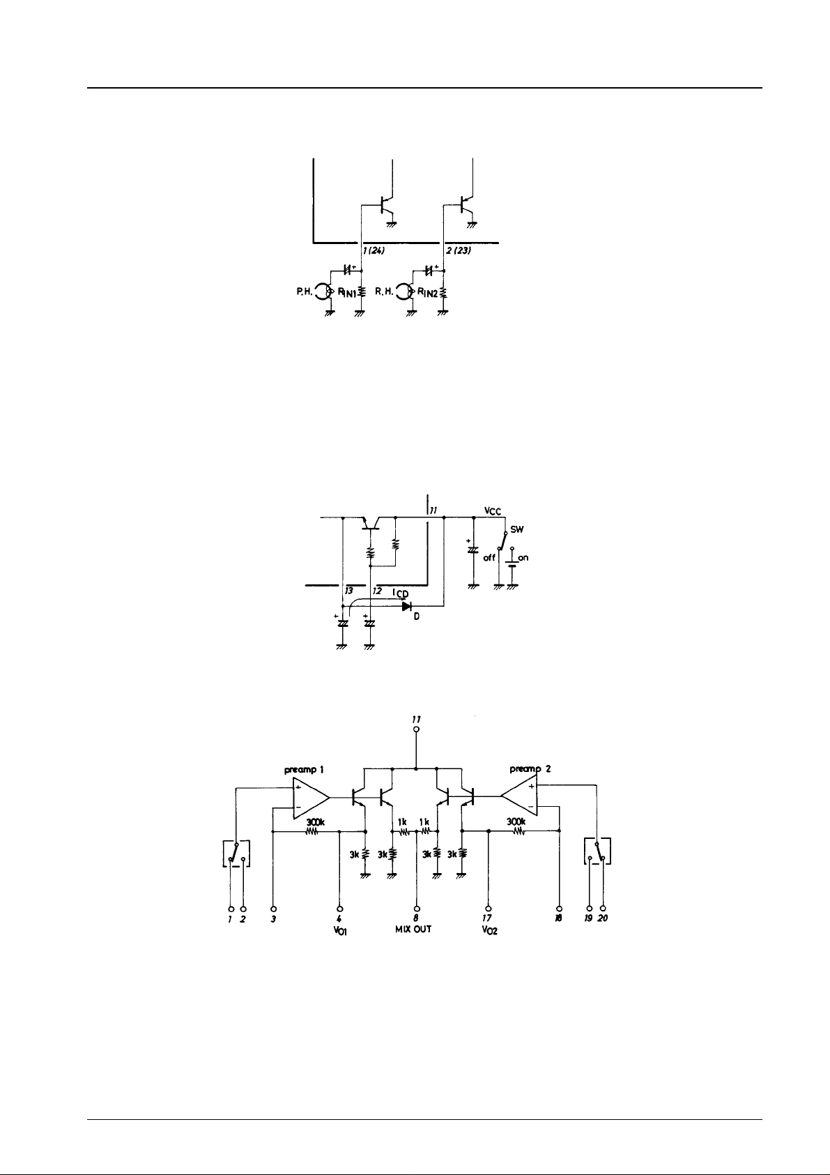
(3) When an electrolytic capacitor is connected to input pins 1, 2 (or 23, 24), make the value of RIN1 as equal to that of RIN2as
possible.
The difference in the value between R
switching. Therefore, the input DC voltage (voltage across R
1 and RIN2 causes the variation in amp output DC voltage at the time of F/R
IN
) must be made as equal as possible.
IN
(4) The amplifier output characteristics are designed to be the same in the Nor Tape/High Speed (pin 15 GND/pin 6 V
Me Tape/Nor Speed (pin 15 V
(5) When externally turning ON/OFF power supply pin 11 (by bringing pin 11 to +V
/pin 6 GND) modes. (Refer to sample application circuit, external constants.)
CC
/GND level) with a capacitor connected
CC
to pin 13, connect external diode D, as shown below, so that no breakdown (or deterioration) of the IC system is caused by
I
when the switch is turned OFF. When no capacitor is connected to pin 13, diode D is not required.
CD
(6) The output MIX circuit is of the emitter follower configuration as shown below.
CC
) and
The MIX OUT output level V
output levels V
V
O
where V
1, VO2 at the time the same input signal is applied to both channels.
O
MIX = 1/2 VO1(= 1/2 × VO2)
1=VO2
O
Unit (resistance: Ω)
MIX at the time a signal is applied to preamp1 (or preamp2) only is 1/2 as compared with
O
No.2651-5/13
Page 6
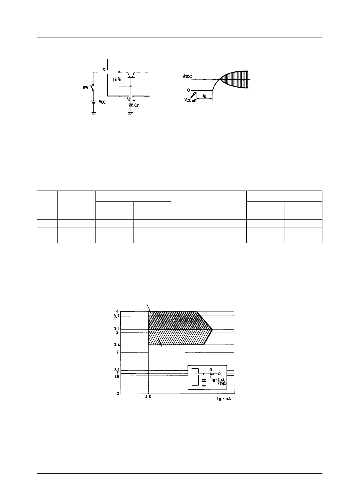
(7) Output waveform starting time
LA3246
Example of rise waveform at pin 4 (or 17)
When supply voltage V
varied by capacitor Cr connected to pin 12.
Refer to Data Cr – t
The minimum value of Cr is 47 µF.
(8) Electronic select switching level
.
The switch level at VCC= 6.0 V is shown below.
Pin Switch Mode
6 Normal/Metal 2.1 V 2.4 V 3.7 V 2 µA Metal Normal
9 Forward/Reverse 2.1 V 3.1 V 3.4 V 2 µA Reverse Forward
15 Normal/Higher 2.1 V 2.4 V 3.7 V 2 µA Higher Normal
As shown above, there is a difference in the switching level at three control pins (6, 9, 15) between operation start and
operation finish.
.
Switching level and mode at each pin (experimental value)
is switched ON, the amplifier output (pins 4, 17) will rise. Output waveform ON time tscan be
CC
.
s
Switching Level
Operation Start
Switching level (reverse) on pin 9 at VCC= 6.0 V, Ta = 25°C
Operation
Finish
Clamp Voltage
Control Current
typ (flow-in)
(at operation
finish)
Mode
(+) (–)
(Metal) (Higher)
Switching level region at pins 6, 15.
No.2651-6/13
Page 7
LA3246
.
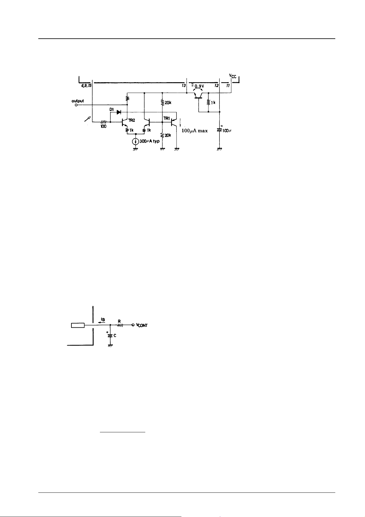
Control circuit
The control circuit for each CONT pin is configured as shown below. When a voltage more than a given value is applied,
the level on the pin is fixed by clamp diode D1.
Current route
Control pin
Description
.
Switching level VSWof the control circuit is fixed by voltage V13 which is 1/2 of the voltage on pin 13.
= 1/2 V13
V
SW
.
Clamp voltage V
= 1/2 × V13 + VD1+VBE1
V
CLP
= 1/2 × V13 + 0.6 (0.3) + 0.6
= 1/2 × V13 + (0.9 or 1.2)
.
The maximum voltage at which the CONT pin is brought to GND level is fixed by the level at which the Q2 is completely
turned OFF.
This level is:
1/2 × V13 – V
Switching is performed at a level less than this.
.
To turn ON/OFF
When turning ON:
at the time a voltage is applied to the CONT pin
CLP
where 0.9 V is for pin 9.
2 = 1/2 × V13 – 0.6 [V]
BE
at clamp mode
1.2 V is for pins 6, 15.
Note: For D1, a Schottky diode is used for pin 9
and a silicon diode is used for pins 6, 15.
Unit (resistance: Ω, capacitance: F)
.
V
min=R×IBmax + Operation finish voltage.
CONT
I
=4µA
B
Operation finish voltage
Pins 6, 15 : = 1/2 × V13
Pin 9 : = 1/2 × V13 + V
.
V
max=R×IBmax + Clamp voltage
CONT
When the supply voltage is fixed, clamp voltage V
resistor R is restricted by V
I
max = 100 µA ^
B
The minimum value of resistor R is fixed by this equation.
Example
Assuming V
Therefore, R = 100 kΩ presents no problem.
When turning OFF:
Bring the level on the CONT pin to a level less than:
1/2 × V13 – V
= 1/2 × V13 + 0.6 [V]
R is restricted by I
CONT
V
CONT
=10V,V
CC
2 = 1/2 × V13 – 0.6 [V]
BE
BE
max.
B
max. as shown below.
max – V
R
max = 10 V, Rmin is 50 kΩ.
CONT
CLP
CLP
is fixed. When resistor R is fixed based on a balance with capacitor C,
To turn ON the control circuit to finish the
operation, I
V
OUT
is required. Control voltage
B
is obtained with IBof 4 µA min.
No.2651-7/13
Page 8
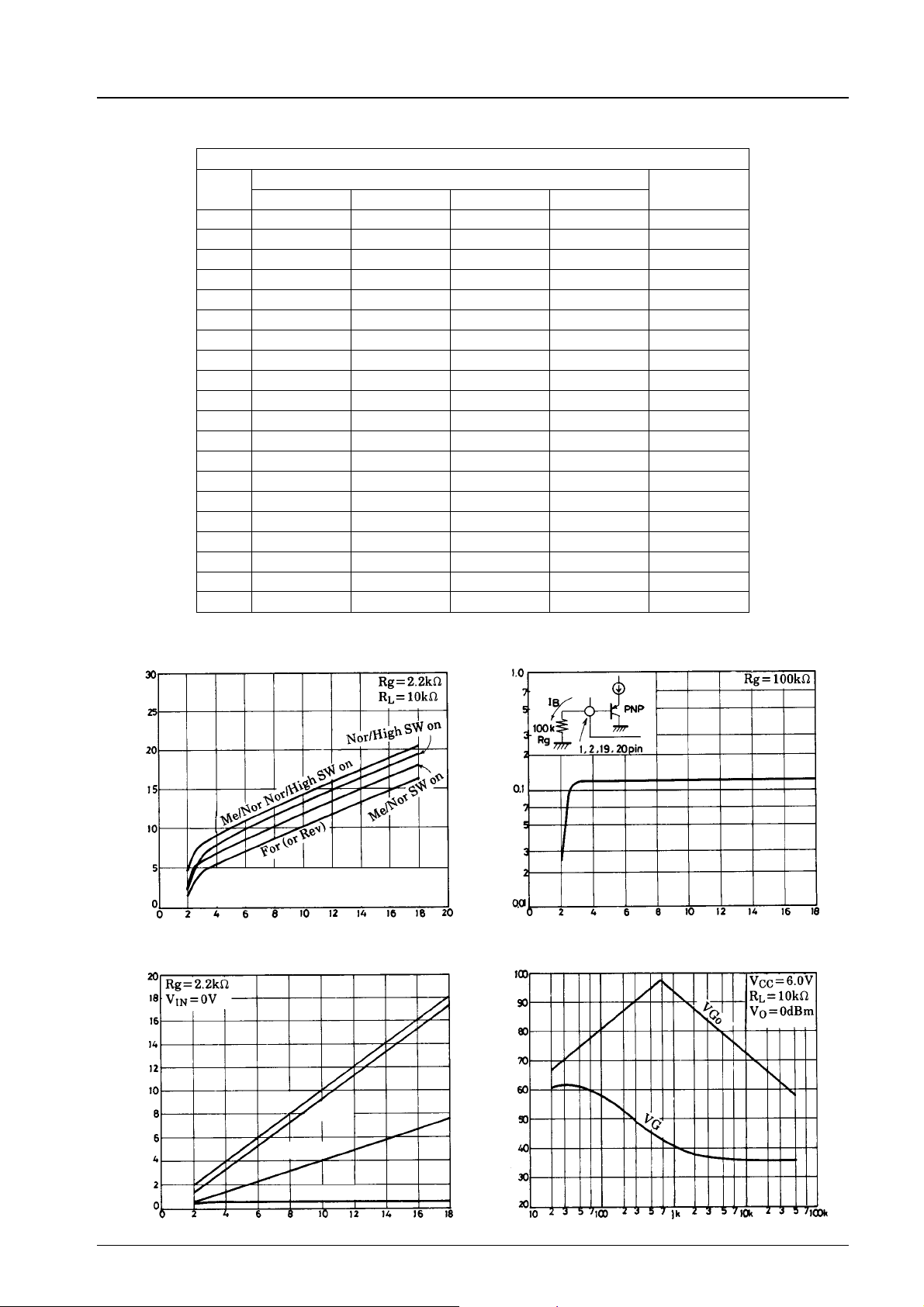
(9) Example of voltage on each pin
Pin
1 0.3 0.3 0.3 0.3 mV
2 0.3 0.3 0.3 0.3 mV
3 0.59 0.58 0.57 0.56 V
4 1.63 2.23 3.65 5.02 V
5 1.63 2.23 3.65 5.02 V
6 (GND) 0 (GND) 0 (GND) 0 (GND) 0 V
70000V
8 1.63 2.29 3.64 5.01 V
9 (GND) 0 (GND) 0 (GND) 0 (GND) 0 V
10 (GND) 0 (GND) 0 (GND) 0 (GND) 0 V
11 V
12 4.48 5.96 8.97 11.23 V
13 3.72 5.20 8.21 11.98 V
140000V
15 (GND) 0 (GND) 0 (GND) 0 (GND) 0 V
16 1.63 2.23 3.65 5.02 V
17 1.63 2.23 3.65 5.02 V
18 0.59 0.58 0.57 0.56 V
19 0.3 0.3 0.3 0.3 mV
20 0.3 0.3 0.3 0.3 mV
4.5 V 6.0 V 9.0 V 12.0 V
LA3246
Rg = 2.2 kΩ, Ta = 25°C, VIN= 0, pins 6, 9 and 15 = GND
CC
–V
V
CC
V
CC
Supply voltage, V
V
CC
CC
Unit
V
Quiescent current, Iccs (Electronic SW ON) – mA
Quiescent current, Icco – mA
–V
DC
Iccs, Icco – V
Nor/High and Me/Nor SW on: Pins 6 and
15 are brought to supply voltage level.
CC
Supply voltage, VCC–V
V
DC–VCC
Pin 12
Pin 13
–µA
Input bias current, I
IB–V
CC
B
Supply voltage, VCC–V
VGo, VG – f
i
DC voltage, V
Pins 4, 19
Pins 3,18
Supply voltage, VCC–V
Voltage gain (open), VGo – dB
Voltage gain (closed), VG – dB
Input frequency, fi–Hz
No.2651-8/13
Page 9
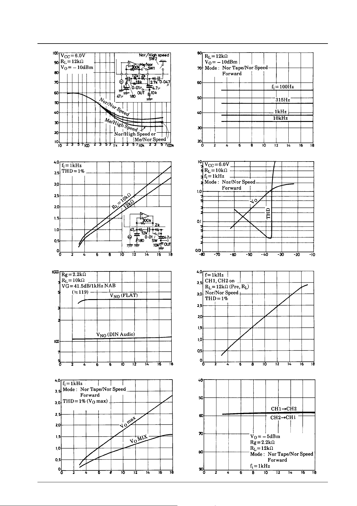
LA3246
Voltage gain (closed), VG – dB
max–V
O
VG–f
i
Input frequency, fi–Hz
VOmax–V
CC
–V
O
VG–V
CC
Voltage gain (closed), VG – dB
Supply voltage, VCC–V
VO,THD–V
IN
Maximum output voltage, V
–µV
NO
Output noise voltage, V
MIX–V
O
Supply voltage, VCC–V
VNO–V
CC
Supply voltage, VCC–V
VOmax, VOMIX–V
CC
Output voltage, V
Total harmonic distortion, THD – %
MIX–V
O
Pin 8 voltage, V
Input voltage, VIN– dBm
V
MIX–V
O
CC
Supply voltage, VCC–V
CT1–V
CC
CH1 only operated
max, V
O
Maximum output voltage, V
Supply voltage, V
CC
–V
Crosstalk (between channels), CT1 – dB
Supply voltage, VCC–V
No.2651-9/13
Page 10
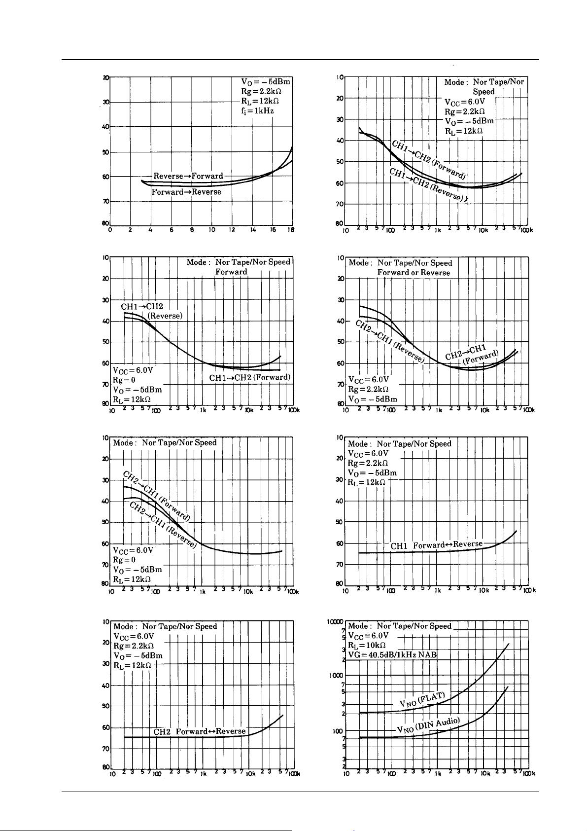
CT2–dB
CT2–V
CC
LA3246
CT3–f
i
Crosstalk (between forward and reverse),
c
Crosstalk (between channels), CT4 – dB
Supply voltage, VCC–V
CT4–f
Input frequency, f
CT6–f
i
i
–Hz
i
Crosstalk (between channels), CT3 – dB
Input frequency, fi–Hz
CT5–f
i
Crosstalk (between channels), CT5 – dB
Input frequency, fi–Hz
CT7–f
i
CT7 –dB
Crosstalk (between channels), CT6 – dB
CT8–dB
CH2 crosstalk (between forward and reverse),
Input frequency, fi–Hz
CT8–f
i
Input frequency, fi–Hz
CH1 Crosstalk (between forward and reverse),
–µV
NO
Output noise voltage, V
Input frequency, fi–Hz
–Rg
V
NO
Signal source resistance, Rg – Ω
No.2651-10/13
Page 11
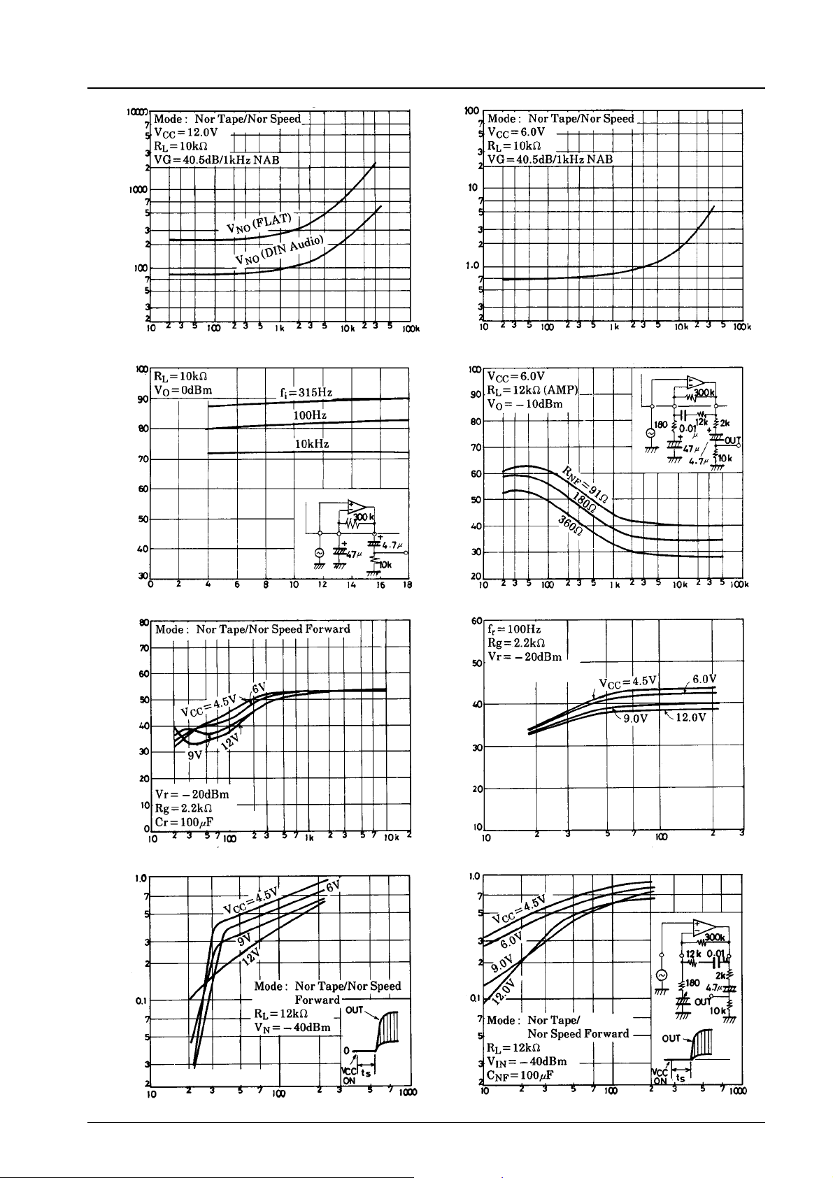
LA3246
–µV
Output noise voltage, V
NO
VNO–Rg
VNI–Rg
–µV
NI
Equivalent input noise voltage, V
Signal source resistance, Rg – Ω Signal source resistance, Rg – Ω
VGo–V
CC
VG–f
i
Voltage gain (open), VGo – dB
Ripple rejection ratio, Rr – dB
– sec
S
Supply voltage, VCC–V
Rr –f
r
(Pin 12)
Ripple frequency, fr–Hz
tS–Cr
Voltage gain (closed), VG – dB
Cr = 47 µF or greater
Ripple rejection ratio, Rr – dB
Capacitor for ripple filter (pin 12), Cr – µF
– sec
S
Input frequency, fi–Hz
Rr–Cr
tS–C
NF
Starting time, t
Cr = 47 µF or greater
Capacitor for ripple filter (pin 12), Cr – µF
Starting time, t
or less
Reverse transfer capacitance, CNF–µF
No.2651-11/13
Page 12
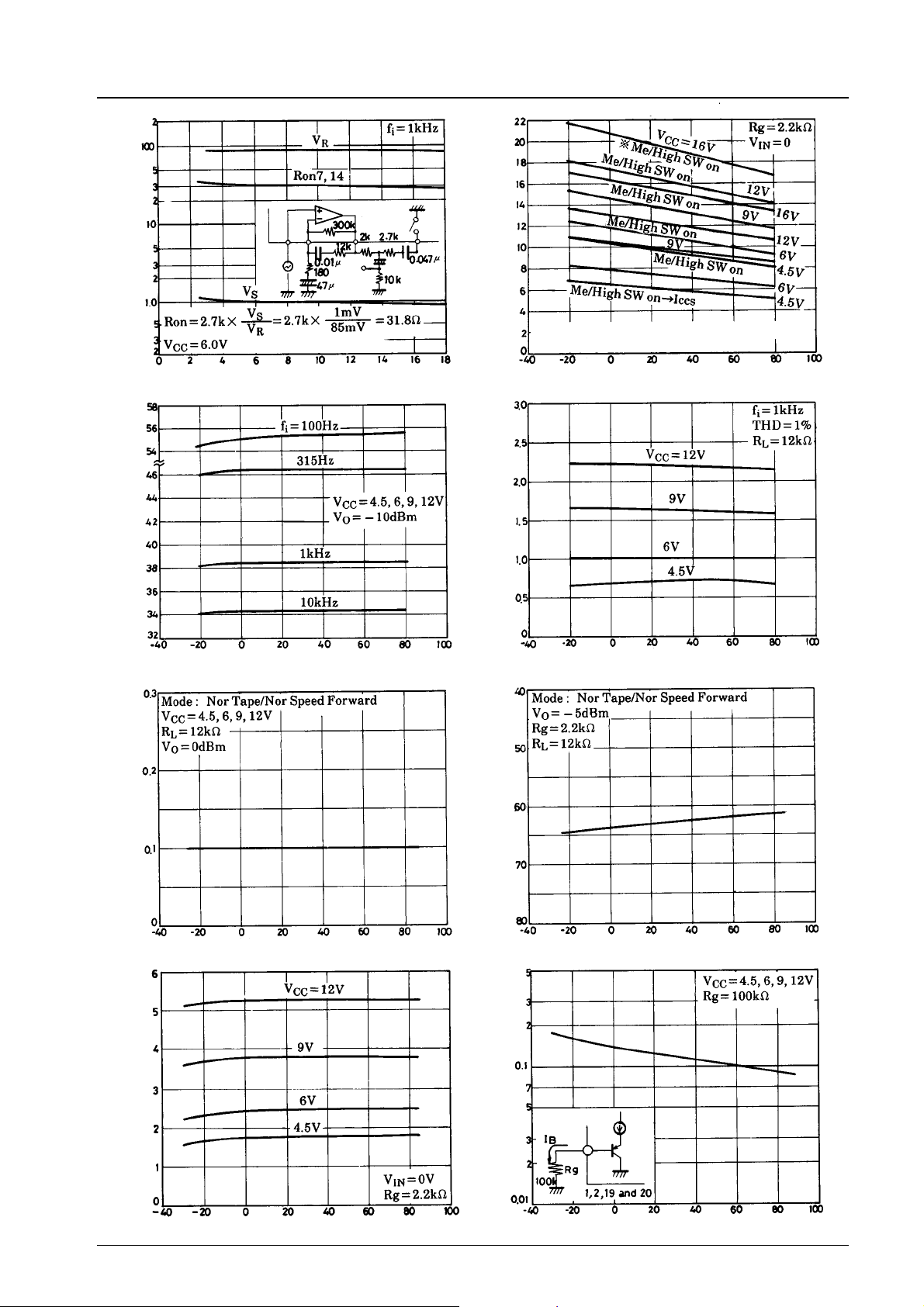
LA3246
Ron,V–V
Voltage drop,V–mV
ON Resistance, Ron – Ω
VR: Voltage across 2.7 kΩ resistor
CC
Quiescent current, Iccs – mA
* Me/High SW on: Pins 6, 15 are
Quiescent current, Icco – mA
brought to supply voltage level.
Supply voltage, VCC–V
VG–Ta
Iccs, Icco – Ta
Ambient temperature, Ta – °C
VOmax–Ta
max–V
O
Voltage gain (closed), VG – dB
–V
BL
Channel balance, V
–V
ODC
Ambient temperature, Ta – °C
VBL–Ta
Ambient temperature, Ta – °C
V
–Ta
ODC
Maximum output voltage, V
Crosstalk (between channels), CT9 – dB
–µA
Ambient temperature, Ta – °C
CT9–Ta
Ambient temperature, Ta – °C
IB–Ta
B
DC voltage, V
Input bias current, I
Ambient temperature, Ta – °C
Ambient temperature, Ta – °C
No.2651-12/13
Page 13

LA3246
No products described or contained herein are intended for use in surgical implants, life-support systems,
aerospace equipment, nuclear power control systems, vehicles, disaster/crime-prevention equipment and the like,
the failure of which may directly or indirectly cause injury, death or property loss.
Anyone purchasing any products described or contained herein for an above-mentioned use shall:
1 Accept full responsibility and indemnifyanddefend SANYO ELECTRIC CO., LTD., its affiliates, subsidiaries and
distributors and all their officers and employees, jointly and severally, against any and all claims and litigation
and all damages, cost and expenses associated with such use:
2 Not impose any responsibility for any fault or negligence which may be cited in any such claim or litigation on
SANYO ELECTRIC CO., LTD., its affiliates, subsidiaries and distributors or any of their officers and employees
jointly or severally.
Information (including circuit diagrams and circuit parameters) herein is for example only; it is not guaranteed for
volume production. SANYO believes information herein is accurate and reliable, but no guarantees are made or
implied regarding its use or any infringements of intellectual property rights or other rights of third parties.
This catalog provides information as of December, 1997. Specifications and information herein are subject to change without notice.
No.2651-13/13
 Loading...