

Page 1
Monolithic Linear IC
Ordering number : EN4530A
53096HA (OT) No. 4530-1/13
SANYO Electric Co.,Ltd. Semiconductor Bussiness Headquarters
TOKYO OFFICE Tokyo Bldg., 1-10, 1 Chome, Ueno, Taito-ku, TOKYO, 110 JAPAN
1.5 V Record Preamplifier
LA3235W
Overview
The LA3235W is a single-chip record system IC for use in
1.5 V headphone stereo products. While previous
recording systems were implemented using a dedicated
tape drive, by using the LA3235W, such a system can be
implemented by adding electronic switching to a
playback-only tape drive. Additionally, a compact
record/playback system can be implemented with just two
chips by combining this IC and the LA4590W 1.5 V
preamplifier/power amplifier IC
Functions
• Microphone amplifier (with ALC) ×2
• Microphone monitor amplifier ×2
• Radio amplifier (with ALC) × 2
• Record bias power supply
• Record amplifier ×4 (with forward/reverse switching
and muting functions)
• Microphone power supply
• All control circuits, including electronic switching
circuits, built in
Features
• Miniature package (48-pin SQFP)
• Built-in microphone and record bias power supplies
• Built-in radio amplifier with ALC circuit
• Systems can be easily controlled from a microprocessor
using the built-in electronic switching, power supply,
and amplifier block control circuits.
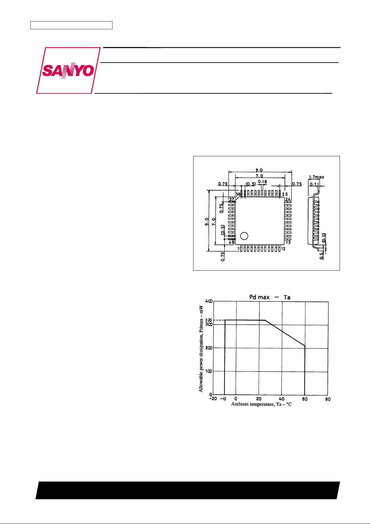
Package Dimensions
unit: mm
6134A-SQFP48
SANYO: SQFP48
[LA3235W]
Page 2

Specifications
Absolute Maximum Ratings at Ta = 25°C
Operating Conditions at Ta = 25°C
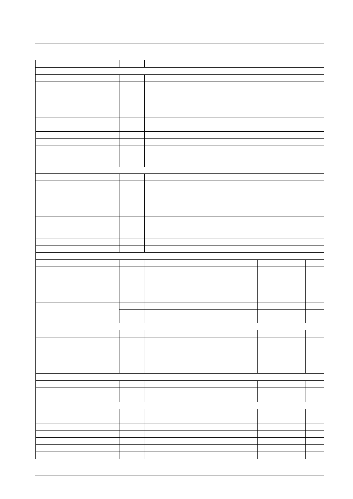
Operating Characteristics at Ta = 25°C, VCC1 and V
CCRF
= 1.2 V, VCC2 = 2.4 V, f = 1 kHz, 0 dBm = 0.775 V,
R
LMIC
= 10 kΩ, R
LRadio
= 10 kΩ, R
LMON
= 10 kΩ, R
LREC
= 3 kΩ
No. 4530-2/13
LA3235W
Parameter Symbol Conditions Ratings Unit
Maximum supply voltage V
CC
max 4.5 V
Allowable power dissipation Pd max 320 mW
Operating temperature Topr –10 to +65 °C
Storage temperature Tstg –40 to +125 °C
Parameter Symbol Conditions Ratings Unit
Recommended supply voltage
V
CC
1, V
CCRF
1.5 V
V
CC
2 2.4 V
Operating supply voltage range
V
CC
1, V
CCRF
0.9 to 2.2 V
V
CC
2 2.0 to 4.0 V
Parameter Symbol Conditions min typ max Unit
No signal supply current: record/V
CC
1 I
CCR1
Microphone Rg = 6.8 kΩ 0.08 0.13 0.23 mA
No signal supply current: record/V
CCRF
I
CCRR
Microphone Rg = 6.8 kΩ 2.0 3.5 5.0 mA
No signal supply current: record/V
CC
2 I
CCR2
Microphone Rg = 6.8 kΩ 0.85 1.5 2.1 mA
No signal supply current: playback/V
CC
1 I
CCP1
0.1 5.0 µA
No signal supply current: playback/V
CCRF
I
CCPR
0.36 0.6 1.0 mA
No signal supply current: playback/V
CC
2 I
CCP2
0.3 0.5 0.75 mA
[Microphone amplifier] (measured with ALC off)
Voltage gain (closed) VG
M
VO= –20 dBm 35 dB
Maximum output voltage V
O maxM
THD = 1% 320 mV
Total harmonic distortion THD
M
VO= 200 mV 0.1 %
Output noise voltage V
NOM
Rg = 6.8 kΩ, BPF = 20 Hz to 20 kHz 130 µV
Crosstalk (interchannel) CT
M
VO= –20 dBm, TUNE 1 KHz 46 dB
Ripple rejection ratio SVRR
M
Rg = 6.8 kΩ, fR = 100 Hz, VR = –30 dBm 37 dB
[Radio Amplifier] (measured with ALC off)
Voltage gain (closed) VG
R
VO= –20 dBm 14.5 dB
Maximum output voltage V
O maxR
THD = 1% 320 mV
Total harmonic distortion THD
R
VO= 200 mV 0.1 %
Output noise voltage V
NOR
Rg = 6.8 kΩ, BPF = 20 Hz to 20 kHz 30 µV
Crosstalk (interchannel) CT
R
VO= –20 dBm, TUNE 1 KHz 59 dB
Ripple rejection ratio SVRR
R
Rg = 6.8 kΩ, fR = 100 Hz, VR = –30 dBm 55 dB
[Monitor Amplifier]
Voltage gain (closed) VG
MONVO
= –20 dBm 9.5 dB
Maximum output voltage V
OMON
THD = 1% 260 mV
Total harmonic distortion THD
MONVO
= 100 mV 0.1 %
Output noise voltage V
NOMON
BPF = 20 Hz to 20 kHz 11 µV
Crosstalk (interchannel) CT
MONVO
= –20 dBm 59 dB
Ripple rejection ratio SVRR
MONfR
= 100 Hz, VR = –30 dBm 57 dB
[Record Amplifier]
Voltage gain (closed) VG
RECVO
= –10 dBm 22 dB
Maximum output voltage V
OREC
THD = 1% 670 mV
Total harmonic distortion THD
RECVO
= 300 mV 0.08 %
Output noise voltage V
NOREC
BPF = 20 Hz to 20 kHz 46 µV
Crosstalk (interchannel) CT
RECVO
= –10 dBm 55 dB
Ripple rejection ratio SVRR
RECfR
= 100 Hz, VR = –30 dBm 55 dB
Continued on next page.
Page 3
Continued form preceding page.
No. 4530-3/13
LA3235W
Parameter Symbol Conditions min typ max Unit
[Microphone + Record]
Voltage gain (closed) VG
MR
VO= –10 dBm, ALC OFF 52 56.6 60 dB
Maximum output voltage V
OMR
THD = 3% 500 700 mV
Total harmonic distortion THD
MR
Vi = –40 dBm 0.55 1.3 %
ALC voltage ALCV
MR
Vi = –40 dBm, Rg = 6.8 kΩ 300 400 500 mV
ALC balance ALCB
MR
Vi = –40 dBm, Rg = 6.8 kΩ 0 1.5 dB
ALC start input ALCI
MR
–65.5 –62.5 –59.5 dBm
ALC width ALCW
MR
Input level relative to the ALC start point such
35 42 dB
that the output is +3 dB.
Output noise voltage V
NOMR
Rg = 6.8 kΩ, BPF = 20 Hz to 20 kHz 1.5 2.8 mV
Crosstalk (interchannel) CT
MR
Vi = –40 dBm 11 19 dB
SVRR
MR1
Rg = 6.8 kΩ, fR= 100 Hz, VR = –30 dBm 10 16 dB
Ripple rejection ratio
SVRR
MR2
Rg = 6.8 kΩ, fR= 100 Hz, VR = –20 dBm
50 58 dB
With ripple added to V
CC
2, TUNE = 100 Hz
[Radio + Record]
Voltage gain VG
RR
VO= –10 dBm, ALC OFF 31.5 35.5 39.5 dB
Maximum output voltage V
ORR
THD = 3% 470 570 mV
Total harmonic distortion THD
RR
Vi = –30 dBm 0.55 1.3 %
ALC voltage ALCV
RR
Vi = –30 dBm, Rg = 6.8 kΩ 300 410 500 mV
ALC balance ALCB
RR
Vi = –30 dBm, Rg = 6.8 kΩ 0 1.5 dB
ALC start input ALCI
RR
–45.5 –42.5 –39.5 dBm
ALC width ALCW
RR
Input level relative to the ALC
35 40 dB
start point such that the output is +3 dB.
Output noise voltage V
NORR
Rg = 6.8 kΩ, BPF = 20 Hz to 20 kHz 340 610 µV
Crosstalk (interchannel) CT
RR
Vi = –30 dBm 35 47 dB
Ripple rejection ratio SVRR
RR
Rg = 6.8 kΩ, fR= 100 Hz, VR = –30 dBm 25 32 dB
[Microphone + Monitor]
Voltage gain (closed) VG
MMONVO
= –20 dBm, ALC OFF 39.5 43.5 47.5 dB
Maximum output voltage V
OMMON
THD = 3% 150 310 mV
Total harmonic distortion THD
MMON
Vi = –40 dBm 0.55 1.3 %
ALC voltage ALCV
MMON
Vi = –40 dB, Rg = 6.8 kΩ 60 90 135 mV
Output noise voltage V
NOMMON
Rg = 6.8 kΩ, BPF = 20 Hz to 20 kHz 350 650 µV
Crosstalk (interchannel) CT
MMON
Vi = –40 dBm 11 19 dB
SVRR
MMON
Rg = 6.8 kΩ, fR= 100 Hz, VR = –30 dBm 21 27 dB
Ripple rejection ratio
SVRR
MMON
Rg = 6.8 kΩ, fR= 100 Hz, VR = –20 dBm
60 70 dB
With ripple added to V
CC
2, TUNE = 100 Hz
[Record Bias Power Supply]
Output voltage V
RBR1IRBR
= –50 mA 0.92 1.0 1.08 V
Ripple rejection ratio SVRR
RBR1
fR = 100 Hz, VR = –30 mA
45 53 dB
I
RBR
= –50 mA, 2SB1295; using 6 ranks
Output voltage V
RBR2
VCC1 = 1.0 V, I
RBR
= 30 mA 0.89 0.93 V
Ripple rejection ratio SVRR
RBR2
VCC1 = 1.0 V, fR = 100 Hz, VR = –30 dBm
33 40 dB
I
RBR
= 30 mA, 2SB1295; using 6 ranks
[Microphone Power Supply]
Output voltage V
MR
I
MR
= 3 mA 1.55 1.65 1.75 V
Ripple rejection ratio SVRR
MR
fR = 100 Hz, VR = –20 dBm
55 70 dB
I
MR
= 3 mA, with ripple added to VCC2
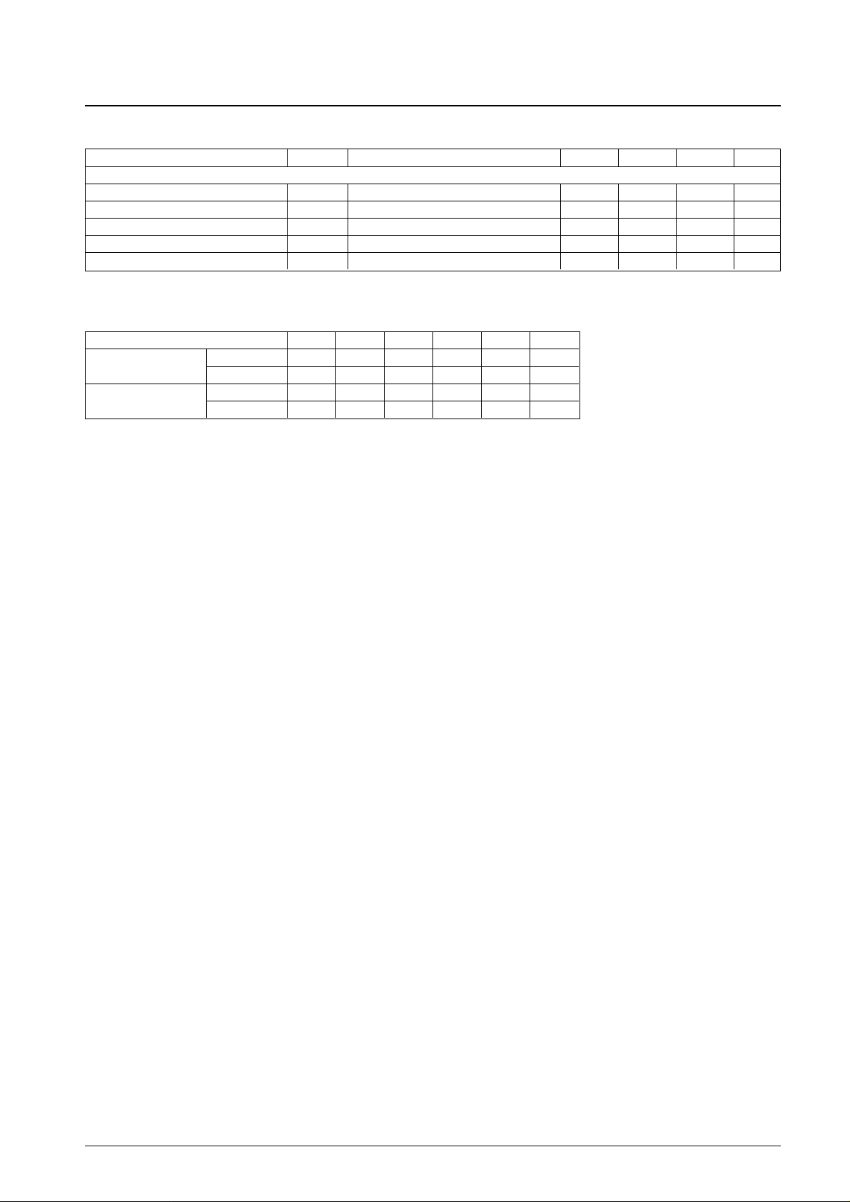
[Switching Control]: Record mode
Forward: CONT A and C pins: source I
FA
, I
FC
Measured with RL= 10 kΩ 20 35 µA
Forward: CONT B pin sink V
FB
I
IN
= 100 µA 64 150 mV
Forward: CONT D pin sink V
FD
I
IN
= 500 µA 110 230 mV
Reverse: CONT B and D pins source I
RB
, I
RD
Measured with RL= 10 kΩ 20 35 µA
Reverse: CONT A pin sink V
RA
I
IN
= 100 µA 64 150 mV
Reverse: CONT C pin sink V
RC
I
IN
= 500 µA 110 230 mV
CONT E pin sink V
E
I
IN
= 100 µA 30 70 mV
Continued on next page.
Page 4
Continued form preceding page.
Switching Control Block: Operating Mode Table
Note: 1. The high-level voltage for A, B, C, D, and E is close to the VCC2 voltage.
2. The high-level voltage for F is close to the V
CCRF
voltage.
No. 4530-4/13
LA3235W
Parameter Symbol Conditions min typ max Unit
[Switching Control]: Playback mode
CONT C and D pins source I
PC
, I
PD
Measured with RL= 10 kΩ 20 35 µA
CONT E pin source I
E
Measured with RL= 10 kΩ 10 18 µA
CONT A and B pins sink V
PA, VPBIIN
= 100 µA 64 150 mV
Radio CONT F pin sink V
RF
IIN= 100 µA 64 150 mV
Microphone CONT F pin V
MF
Vi = –40 dBm, Rg = 6.8 kΩ 1.1 1.2 V
Item A*
1
B*
1
C*
1
D*
1
E*
1
F*
2
REC/MIC/RADIO
FWD H L H L L L
REV L H L H L L
PLAY
MIC L L H H H H
RADIO L L H H H L
Page 5
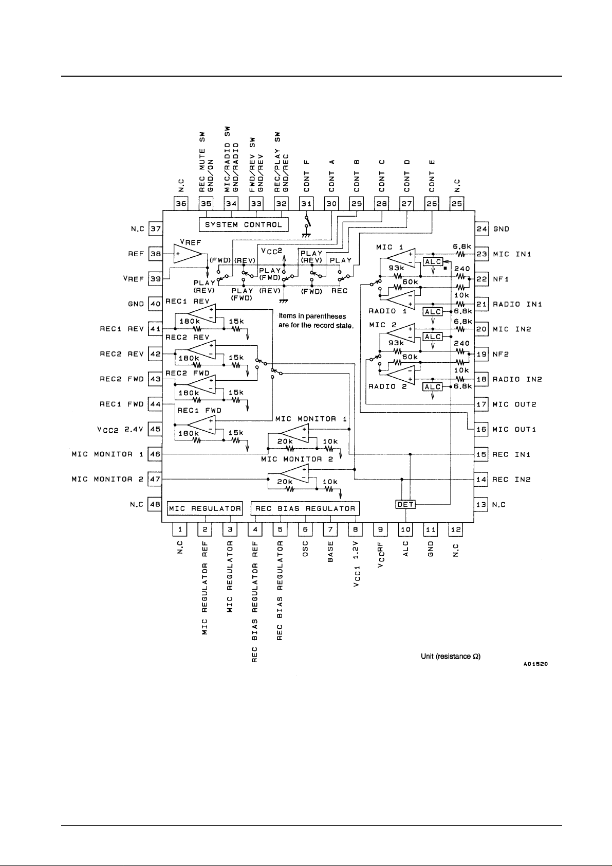
Block Diagram
No. 4530-5/13
LA3235W
Page 6
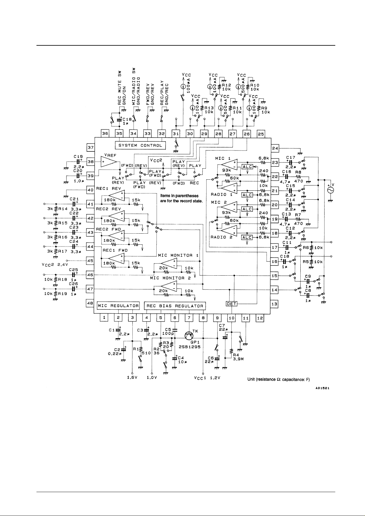
Test Circuit Diagram
No. 4530-6/13
LA3235W
Page 7
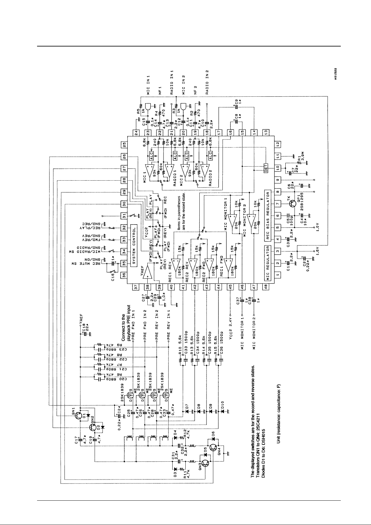
Application Circuit Example 1
No. 4530-7/13
LA3235W
Page 8
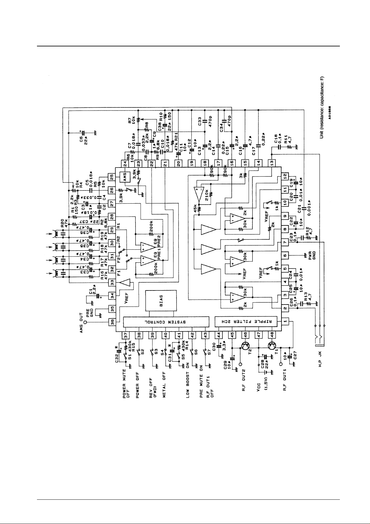
Application Circuit Example 2: Circuit using the LA4590W
No. 4530-8/13
LA3235W
Page 9
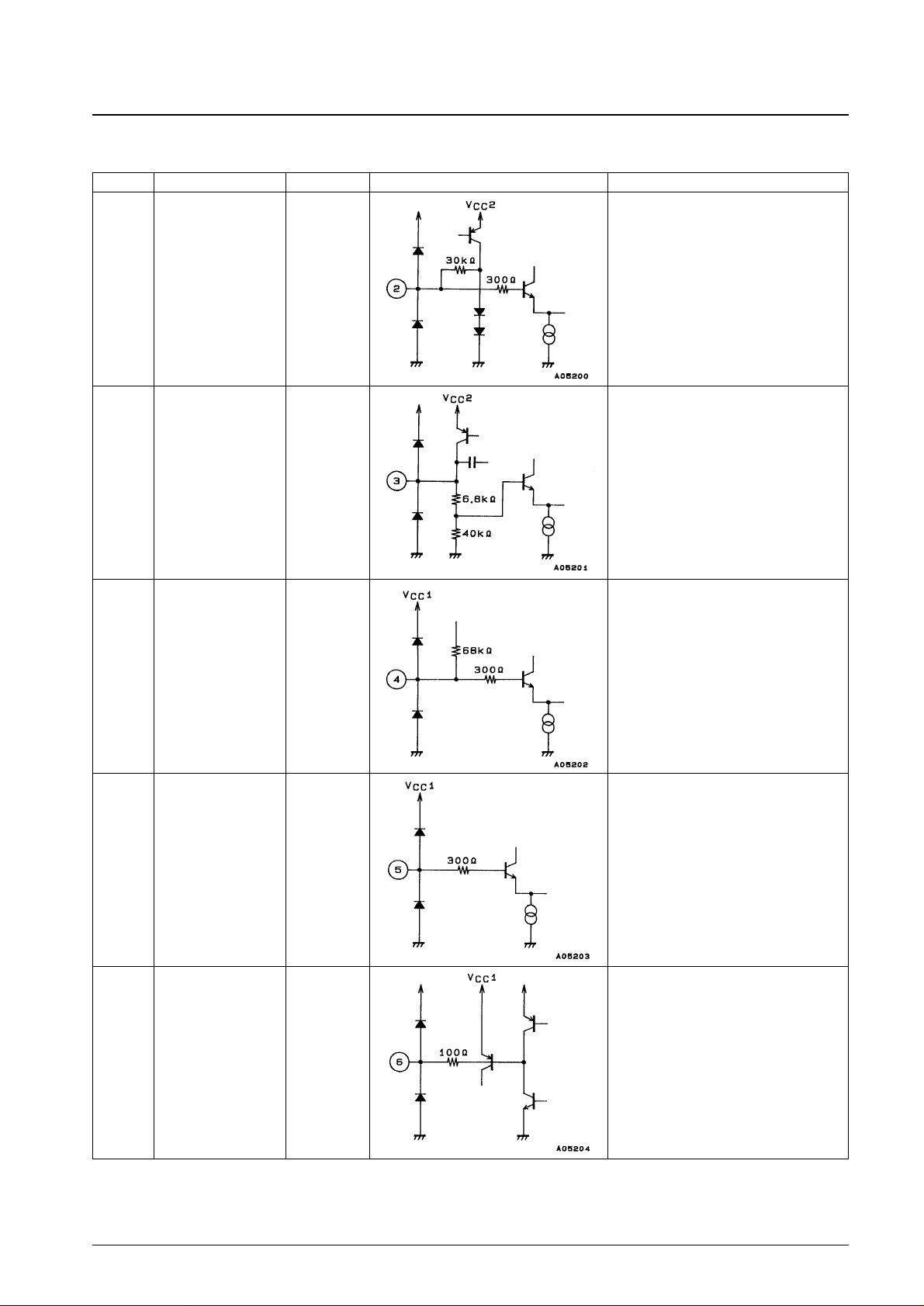
No. 4530-9/13
LA3235W
Pin Functions : The indicated pin voltages are for VCC1 and RF = 1.2 V and VCC2 = 2.4 V.
Pin No. Pin Pin voltage (V) Internal equivalent circuit Notes
2
MIC REGULATOR
REF
1.4
• Microphone power supply reference bias
low-pass filter connection
3 MIC REGULATOR
1.65
• Microphone power supply output
• Always on in record mode
4
REC BIAS
REGULATOR REF
1.0
• Record bias power supply reference bias
low-pass filter connection
• The value of the capacitor connected to this
pin determines the SVRR.
5
REC BIAS
REGULATOR
1.0
• Record bias power supply output
• Always on in record mode
6 OSC
0.5
• Oscillation suppression capacitor
connection
Continued on next page.
Page 10
No. 4530-10/13
LA3235W
Continued form preceding page.
Pin No. Pin Pin voltage (V) Internal equivalent circuit Notes
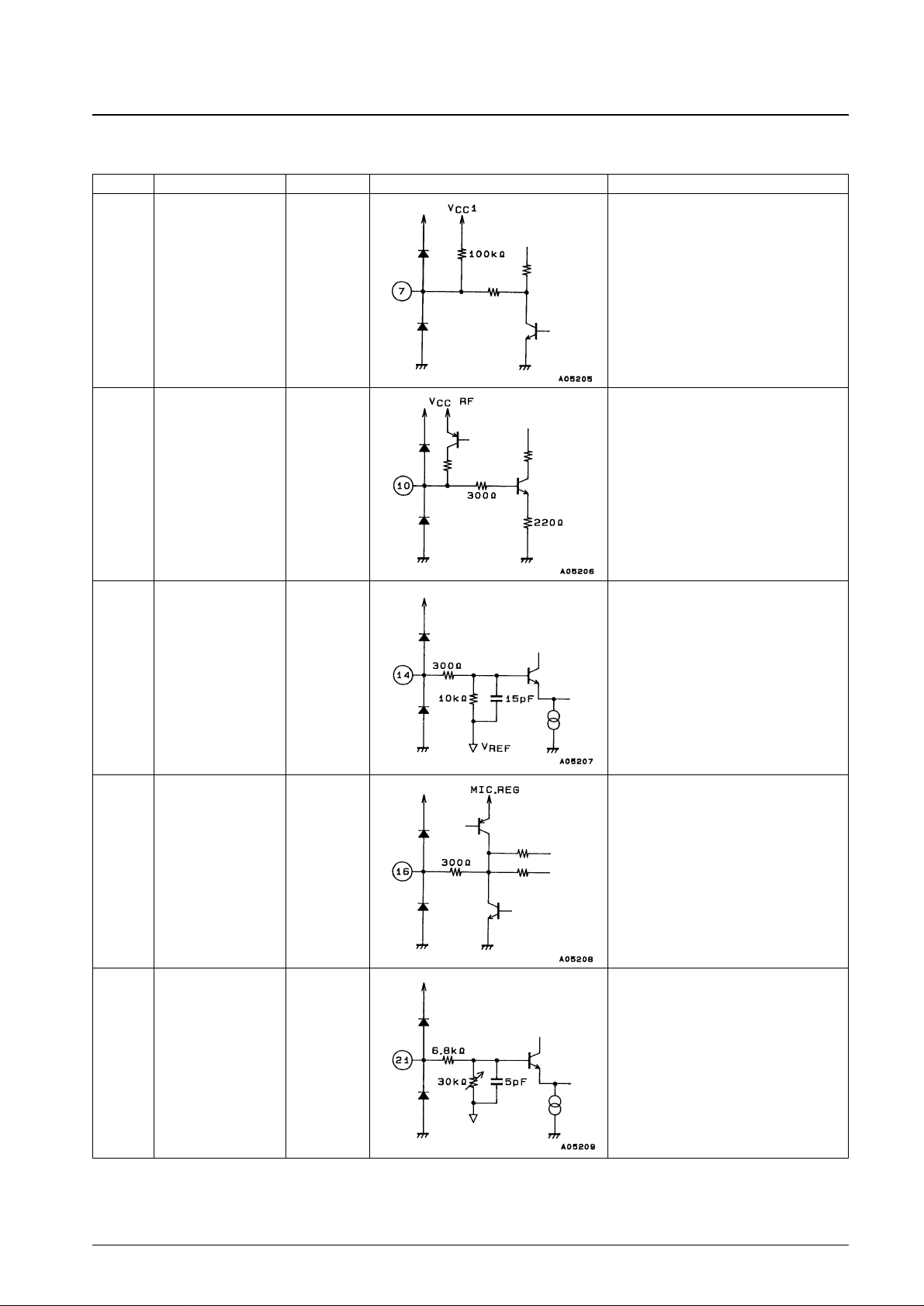
7 BASE
0.55
• External pnp transistor base drive
connection
10 ALC
0.7
• Microphone and radio ALC rectifier
connection
• The external resistor and capacitor
connected to this pin determine the ALC
attack and recovery times.
14
15
REC IN2
REC IN1
0.8
• Record amplifier and microphone monitor
amplifier inputs
• A buzz reduction capacitor is incorporated
in these pin circuits.
• The input resistance is 10 kΩ.
16
17
MIC OUT1
IMC OUT2
0.8
• Microphone and radio amplifier outputs
18
21
RADIO IN2
RADIO IN1
0.8
• Radio amplifier inputs
• The input resistance is variable over the
range 6.8 to 36.8 kΩ.
Continued on next page.
Page 11
No. 4530-11/13
LA3235W
Continued form preceding page.
Pin No. Pin Pin voltage (V) Internal equivalent circuit Notes
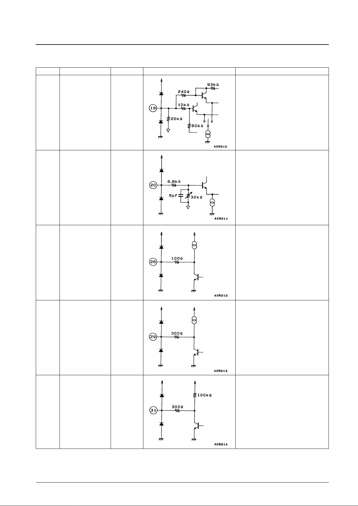
19
22
NF2
NF1
0.8
• Microphone and radio amplifier noise filter
connections
20
23
MIC IN2
MIC IN1
0.8
• Microphone amplifier inputs
• The input resistance is variable over the
range 6.8 to 36.8 kΩ.
26
27
28
CONT E
CONT D
CONT C
VCC2 to 0
• Fixed-current pull-up current sources
Pin 26......................18 µA
Pins 27 and 28........35 µA
29
30
CONT B
CONT A
VCC2 to 0
• 35-µA fixed-current pull-up current sources
31 CONT F
VCCRF to 0
• The pull-up resistor has a value of 100 kΩ
±20%.
Continued on next page.
Page 12
No. 4530-12/13
LA3235W
Continued form preceding page.
Pin No. Pin Pin voltage (V) Internal equivalent circuit Notes
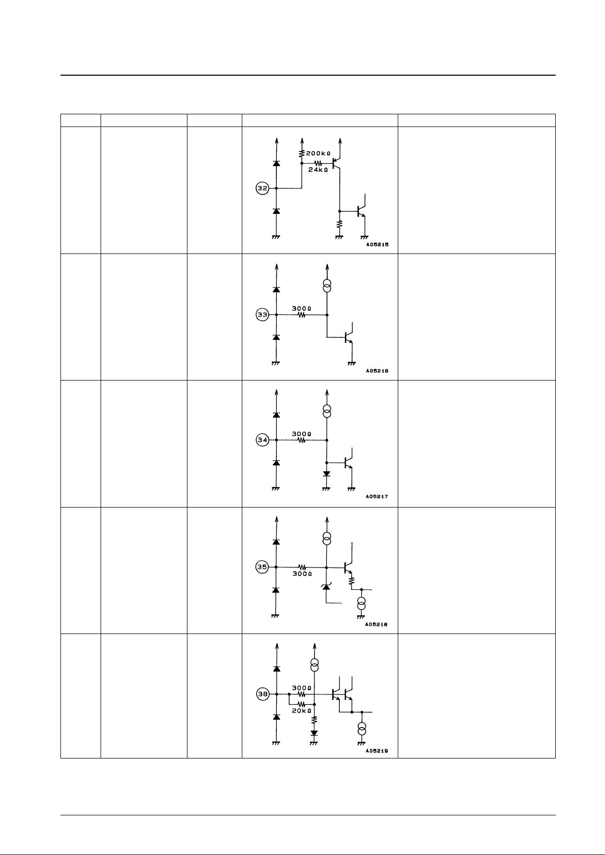
32 REC/PLAY SW
VCCRF to 0
• Sets the system to record mode when
pulled down and to playback mode when
open.
Record mode condition: V32 ≤ 0.1 V
33 FWD/REV SW
0.7 to 0
• Output source current I33≈ 4 µA
• Sets the system to reverse mode when
pulled down.
Reverse mode condition: V33 ≤ 0.4 V
34
MIC/RADIO SW 0.7 to 0
• Output source current I34≈ 8 µA
• Sets the system to radio mode when pulled
down.
Radio mode condition: V34 ≤ 0.4 V
35
REC MUTE SW
VCCRF to 0
• Output source current I35≈ 13 µA
• Sets the system to muted mode when
pulled down.
Muted mode condition: V35 ≤ 0.1 V
38
REF 0.8
• V
REF
amplifier reference bias low-pass
filter connection
Continued on next page.
Page 13
No. 4530-13/13
LA3235W
Continued form preceding page.
Pin No. Pin Pin voltage (V) Internal equivalent circuit Notes
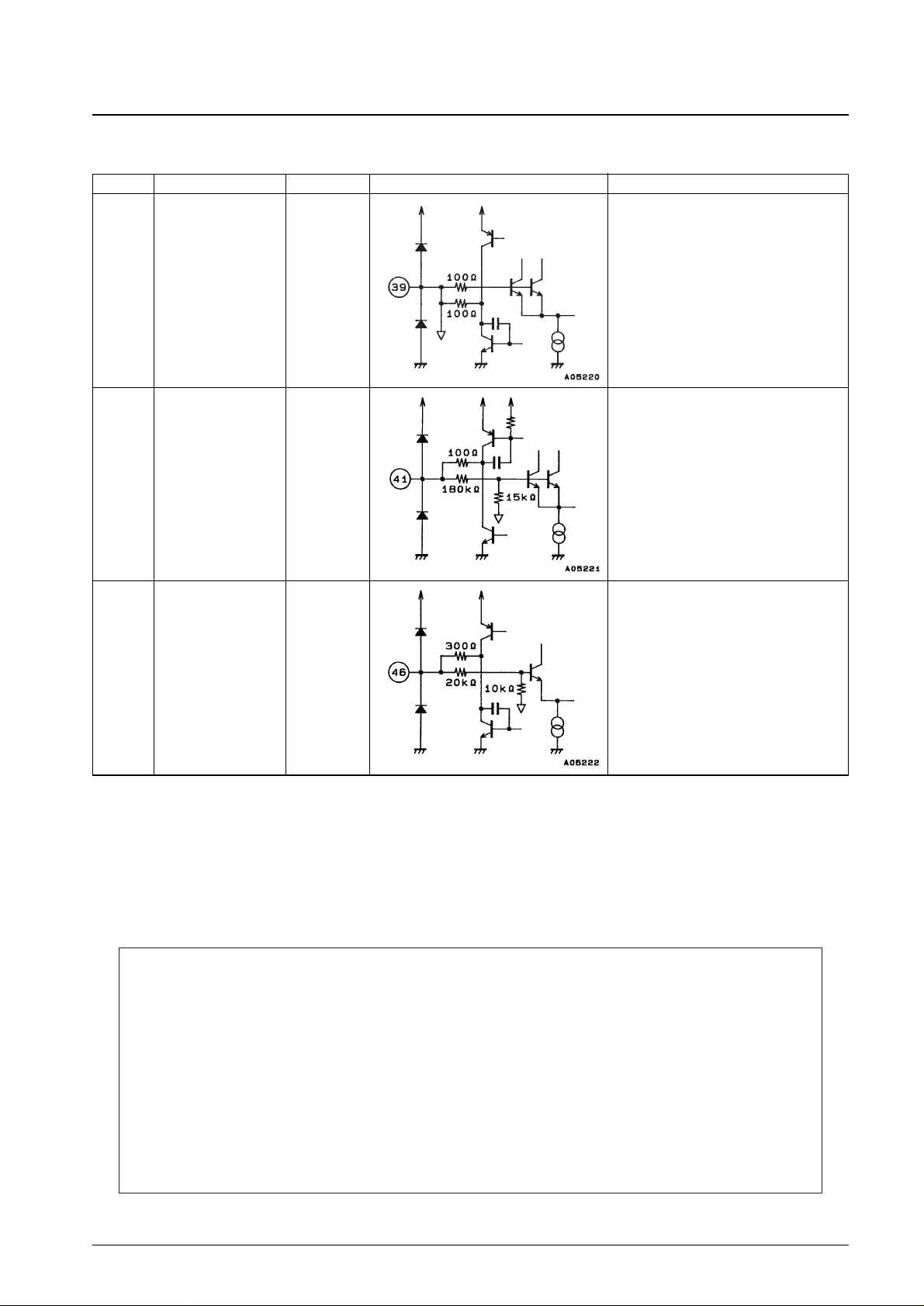
39
V
REF
0.8
• V
REF
amplifier output
• Virtual ground bias for all amplifier blocks
• The V
REF
amplifier makes this a low-
impedance circuit.
41
42
43
44
REC1 REV
REC2 REV
REC2 FWD
REC1 FWD
1.0
• Record amplifier outputs
• The output impedance in playback mode is
195 kΩ ±20%.
46
47
MIC MONITOR 1
MIC MONITOR 2
0.8
• Microphone monitor amplifier output
This catalog provides information as of May, 1996. Specifications and information herein are subject to change
without notice.
■ No products described or contained herein are intended for use in surgical implants, life-support systems, aerospace
equipment, nuclear power control systems, vehicles, disaster/crime-prevention equipment and the like, the failure of
which may directly or indirectly cause injury, death or property loss.
■ Anyone purchasing any products described or contained herein for an above-mentioned use shall:
➀ Accept full responsibility and indemnify and defend SANYO ELECTRIC CO., LTD., its affiliates, subsidiaries and
distributors and all their officers and employees, jointly and severally, against any and all claims and litigation and all
damages, cost and expenses associated with such use:
➁ Not impose any responsibility for any fault or negligence which may be cited in any such claim or litigation on
SANYO ELECTRIC CO., LTD., its affiliates, subsidiaries and distributors or any of their officers and employees
jointly or severally.
■ Information (including circuit diagrams and circuit parameters) herein is for example only; it is not guaranteed for
volume production. SANYO believes information herein is accurate and reliable, but no guarantees are made or implied
regarding its use or any infringements of intellectual property rights or other rights of third parties.
 Loading...